Note: Descriptions are shown in the official language in which they were submitted.
CA 02703543 2010-04-23
WO 2008/055529 PCT/EP2006/010732
1
METHOD AND DEVICE FOR HITLESS TUNABLE OPTICAL FILTERING
* * * * *
Field of the invention
The present invention relates to the field of optical communication systems
including hitless tunable optical filtering functionality, such as hitless
tunable optical
add and/or drop functionality.
Background of the invention
A common technique to increase the transmission capacity of today optical
communication systems is wavelength division multiplexing (WDM), wherein a
plurality of optical channels, each having a respective optical frequency (and
correspondingly respective optical wavelength), are multiplexed together in a
single
optical medium, such as for example an optical fiber. The optical frequencies
allocated
for the WDM channels are typically arranged in a grid having an equal spacing
between
two adjacent frequencies. In dense WDM (DWDM), wherein the WDM channels may
be closely spaced, the frequency spacing is typically equal to about 100 GHz
(corresponding to a wavelength spacing of about 0.8 nm in the near infrared
band -
roughly between 1 1.1m to 2 jim) or about 50 GHz (about 0.4 nm in wavelength).
Other
used WDM channel separations are 200 GHz, 33.3 GHz and 25 GHz. Typically, the
set
of allocated optical frequencies occupies an optical bandwidth of about 4 THz,
which
gives room for the use of up to 40 or 41 WDM channels having 100 GHz spacing.
The
device of the present invention is suitable for a WDM optical bandwidth of at
least
about 1 THz, preferably at least about 2 THz, typically placed around 1550 nm.
Optical networking is expected to be widely used in perspective optical
communication field. The term 'optical network' is commonly referred to an
optical
system including a plurality of point-to-point or point-to-multipoint (e.g.,
metro-ring)
optical systems optically interconnected through nodes. In all-optical
transparent
networks few or no conversions of the optical signal into electrical signal,
and then
again in optical signal, occur along the whole path from a departure location
to a
destination location. This is accomplished by placing at the nodes of the
optical
networks electro-optical or optical devices which are apt to process the
optical signal in
the optical domain, with limited or no need for electrical conversion.
Examples of such
devices are optical add and/or drop multiplexers (OADM), branching units,
optical
CONFIRMATION COPY
CA 02703543 2010-04-23
WO 2008/055529 PCT/EP2006/010732
2
routers, optical switches, optical regenerators (re-shapers and/or re-timers)
and the like.
Accordingly, the term 'optical filtering' or 'optical processing', for the
purpose of the
present description is used to indicate any optical transformation given to an
optical
radiation, such as extracting a channel or a power portion of said channel
from a set of
WDM channels ('dropping'), inserting a channel or a power portion of said
channel into
a WDM signal ('adding'), routing or switching a channel or its power portion
on a
dynamically selectable optical route, optical signal reshaping, retiming or a
combination
thereof. In addition, optical systems, and at a greater extent optical
networks, make use
of optical amplifiers in order to compensate the power losses due to fiber
attenuation or
to insertion losses of the optical devices along the path, avoiding the use of
any
conversion of the optical signal into the electrical domain even for long
traveling
distances and/or many optical devices along the path. In case of DWDM
wavelengths,
all channels are typically optically amplified together, e.g. within a
bandwidth of about
32 nm around 1550 nm.
In optical systems, and at a greater extent in optical networks, a problem
exists
of filtering one or more optical channels at the nodes while minimizing the
loss and/or
the distortion of the filtered optical channel(s), as well the loss and/or the
distortion of
the optical channels transmitted through the node ideally without being
processed
(hereinafter referred to as `thru' channels). Advantageously, the optical
processing node
should be able to simultaneously process more than one channel, each one
arbitrarily
selectable independently from the other processed channels. Ideally up to all
the
channels may be simultaneously selectable to be processed, but in practice a
number
between 2 and 16, preferably between 4 and 8, is considered to be sufficient
for the
purpose.
It is desirable that the optical processing node is tunable or reconfigurable,
i.e., it
can change dynamically the subset of channels on which it operates. In order
to be
suitable to arbitrarily select the channel to be processed within the whole
WDM optical
bandwidth, the tuning range of the whole optical processing node should be at
least
equal to said optical bandwidth.
It is also preferred that while the processing node "moves" from an initial
channel (A) to a destination channel (B), the channels different from A and B
remain
unaffected by the tuning operation. In this case the component is defined as
'hitless'. In
CA 02703543 2015-04-07
3
particular, the channels placed between the initially processed channel and
the final
channel after tuning should not be subject to an additional impairment
penalty, called
'hit', by the tuning operation. The hit may include a loss penalty and/or an
optical
distortion such as phase distortion and/or chromatic dispersion.
For example, optical communication networks need provisions for partially
altering the traffic at each node by adding and/or dropping one or several
independent
channels out of the total number. Typically, an OADM node removes from a WDM
signal a subset of the transmitted channels (each corresponding to one
frequency/wavelength), and adds the same subset with a new information
content, said
subset being dynamically selectable.
There are several additional concerns. The tunable optical processing node
should
not act as a narrow band filter for the unprocessed channels, since
concatenation of such
nodes would excessively narrow the channel pass bands. The tunable optical
processing
node should also be ultra-compact and should have low transmission loss and
low cost,
since these important factors ultimately determine which technology is
selected.
In article "Non-blocking wavelength channel switch using TO effect of double
series coupled microring resonator", S. Yamagata et al., El. Lett. 12th May
2005, Vol. 41,
No. 10, it is demonstrated a non-blocking tunable filter using the thermo-
optic (TO)
effect of a double series coupled polymer microring resonator by controlling
individual
resonant wavelengths.
In article "Fast and stable wavelength-selective switch using double-series
coupled dielectric microring resonator", Y. Goebuchi et al., IEEE Phot. Tech.
Lett., Vol.
18, No. 3, February 1, 2006, it is demonstrated a hitless tunable add-drop
filter using the
thermo-optic effect of double series coupled dielectric microring resonator.
Summary of the invention
In an aspect of the present invention, a method for filtering an optical
signal
comprises a plurality of channels lying on a grid of optical frequencies
equally spaced by
a frequency spacing and occupying an optical bandwidth, comprising: a)
operating an
optical filter comprising a plurality of resonators each having a respective
free spectral
range, wherein a first resonator of said plurality is optically coupled to the
optical signal
and the remaining resonators of said plurality are optically coupled in series
to said first
.k CA 02703543 2015-04-07
3a
resonator, so that a respective resonance of each one of said plurality of
resonators falls
within a first frequency band having bandwidth less than or equal to 15 GHz;
b)
operating said optical filter so as to obtain a separation between said
respective resonance
of at least one resonator with respect to said respective resonance of at
least another
different resonator, said separation being greater than or equal to 25 GHz; c)
operating
said optical filter so that said respective resonance of each one of said
plurality of
resonators falls within a second frequency band, different from the first
frequency band,
having bandwidth less than or equal to 15 GHz, wherein during the procedure
from step
a) to step c), at least one among said respective resonance of said at least
one resonator
and said respective resonance of said at least another different resonator is
moved also
outside a frequency region spanning between, and including, the first and the
second
frequency band.
In an another aspect of the present invention, an optical device comprises: an
optical filter having: an input port for receiving an optical signal
comprising a plurality of
channels lying on a grid of optical frequencies equally spaced by a frequency
spacing and
occupying an optical bandwidth, and an output port; a first optical path
optically
connecting said input port to said output port; a plurality of resonators each
having a
respective free spectral range, wherein a first resonator of said plurality is
optically
coupled to the first optical path and the remaining resonators of said
plurality are
optically coupled in series to said first resonator; a control system
operatively connected
to the plurality of resonators of the optical filter, said control system
being configured to
perform the steps of: a) operating the optical filter so that a respective
resonance of each
one of said plurality of resonators falls within a first frequency band having
bandwidth
less than or equal to 15 GHz; b) operating said optical filter so as to obtain
a separation
between said respective resonance of at least one resonator with respect to
said respective
resonance of at least another different resonator, said separation being
greater than or
equal to 25 GHz; c) operating said optical filter so that said respective
resonance of each
one of said plurality of resonators falls within a second frequency band,
different from
the first frequency band, having bandwidth less than or equal to 15 GHz,
wherein during
the procedure from step a) to step c), at least one among said respective
resonance of said
at least one resonator and said respective
CA 02703543 2014-08-18
3b
resonance of said at least another different resonator is moved also outside
the frequency
region comprised between, and including, the first and the second frequency
band.
The Applicant has found that there is a need for an optical communication
system
having tunable optical processing functionality which leaves unaltered, or at
least reduces
the alteration of, the thru channels during tuning, i.e. it should be ideally
hitless. In
addition, the optical processing node should preferably be low-loss, low-cost,
fast tunable
and/or broadband.
The Applicant has noted that the filter devices described in the above cited
CA 02703543 2010-04-23
WO 2008/055529 PCT/EP2006/010732
4
articles are not optimally designed and/or operated for changing (tuning) the
filtered
optical channel from an initial channel to a final one while keeping at zero
or low level
the power and/or dispersion hit on the thru channels (placed in between the
initial and
final channel and/or outside the spectral region spanning from the initial to
the final
channel) during the entire tuning procedure.
The Applicant has found a method and a system for optical transmission
provided with tunable optical processing functionality which can solve one or
more of
the problems stated above. The solution of the present invention is simple,
feasible and
low cost.
In an aspect of the present invention, a method for filtering an optical
signal as
set forth in appended claim 1 is provided.
The applicant believes that, during tuning of an optical filter comprising a
plurality of resonators, the fact that a resonance of at least one resonator
is moved
outside the frequency region strictly necessary for going from the initial
channel to the
final one, allows achieving 'hitless' or low hit tuning of the overall filter.
Advantageous
embodiments of this method are provided as set forth in appended claims 2 to
15.
According to another aspect of the present invention, an optical device for
filtering an optical signal as set forth in appended claim 16 is provided.
Advantageous
embodiments of this method are provided as set forth in appended claims 17 to
29.
According to a further aspect of the present invention, as set forth in claim
30, an
optical communication system comprises a transmitter, a receiver, an optical
line
optically connecting the transmitter and the receiver and an optical device
according to
the above and coupled along the optical line.
Brief description of the drawings
The features and advantages of the present invention will be made clear by the
following detailed description of an embodiment thereof, provided merely by
way of
non-limitative example, description that will be conducted making reference to
the
annexed drawings, wherein:
Figure 1 schematically shows in terms of functional blocks an exemplary
optical
communication system architecture according to the present invention;
Figure 2 is a schematic diagram showing in terms of functional blocks an
embodiment
of the device for tunable optical filtering according to the present
invention;
CA 02703543 2010-04-23
WO 2008/055529 PCT/EP2006/010732
Figure 3 is a schematic diagram showing in terms of functional blocks a
further
embodiment of the device for tunable optical filtering according to the
present
invention;
Figure 4 shows the principal steps of several comparative examples of a method
for
5 tuning an optical filter.
Figures SA, B, C and D show the effects in terms of optical power responses of
the
methods of Fig. 4.
Figures 6A, B and C show the effects in terms of dispersion responses of the
methods
of Fig. 4.
Figures 7A, 7B and 7C show several embodiments of a method for tuning an
optical
filter in accordance to the present invention.
Figure 8 shows the effects in terms of optical power of the methods of Figs.
7A, B and
C.
Detailed description of the preferred embodiment(s) of the invention
Figure 1 shows an optical communication system architecture according to a
possible embodiment of the present invention.
The optical communication system 100 comprises at least a transmitter 110, a
receiver 120 and an optical line 130 which optically connects the transmitter
and the
receiver. The transmitter 110 is an opto-electronic device apt to emit an
optical signal
carrying information. It typically comprises at least an optical source (e.g.,
a laser) apt
to emit an optical radiation and at least a modulator apt to encode
information onto the
optical radiation. Preferably, the transmitter 110 is a WDM transmitter (e.g.,
a DWDM
transmitter) and the optical signal may comprise a plurality of optical
channels (each
carrying modulation-encoded information) having respective optical frequencies
equally
spaced by a given frequency spacing and occupying an optical bandwidth.
Preferably,
said optical signal lies in the near-infrared wavelength range, e.g. from 900
nm to 1700
nm. Preferably said optical bandwidth is at least 1 THz, more preferably it is
at least 2
THz, still more preferably it is at least 3 THz, such as for example equal to
about 4 THz
(e.g. from about 1530 to about 1560 nm, called C-band). The receiver 120 is a
corresponding opto-electronic device apt to receive the optical signal emitted
by the
transmitter and to decode the carried information. The optical line 130 may be
formed
by a plurality of sections of optical transmission media, such as for example
optical
CA 02703543 2010-04-23
WO 2008/055529 PCT/EP2006/010732
6
fiber sections, preferably cabled. Between two adjacent sections of optical
fiber, an
optical or opto-electronic device is typically placed, such as for example a
fiber splice
or a connector, a jumper, a planar lightguide circuit, a variable optical
attenuator or the
like.
For adding flexibility to the system 100 and improving system functionality,
one
or a plurality of optical, electronic or opto-electronic devices may be placed
along the
line 130. In figure 1 a plurality of optical amplifiers 140 are exemplarily
shown, which
may be line-amplifiers, optical boosters or pre-amplifiers.
According to the present invention, the optical system 100 comprises at least
one
optical processing node (OPN) 150 optically coupled to the optical line 130
and apt to
filter or route or add or drop or regenerate, fully or partially, at least one
optical channel
of the WDM optical signal propagating through the optical line 130. The OPN is
preferably dynamically tunable or reconfigurable. In the particular case
wherein the
optical processing node 150 is an optical add and/or drop node 150, as shown
in Fig. 1,
i.e., a node adapted to route or switch or add and/or drop the optical signal,
the routed or
switched or dropped or added channel(s) may be received or transmitted by
further
receiver(s) 152 or transmitter(s) 154, respectively, which may be co-located
with the
OPN node or at a distance thereof. The optical system or network 100 may
advantageously comprise a plurality of optical processing nodes. In Figure 1 a
further
optical processing node 150' is exemplarily shown, together with its
respective optional
transmitting and receiving devices 152' and 154'.
An optical system 100 having optical add and/or drop nodes 150, as shown in
Figure 1, is commonly referred to as an optical network and it is
characterized by
having a plurality of possible optical paths for the optical signals
propagating through it.
As exemplarily shown in Figure 1, a number of six optical paths are in
principle
possible, which corresponds to all possible choices of the transmitter-
receiver pairs in
Figure 1 (excluding the pairs belonging to the same node).
Figure 2 shows a schematic diagram of an optical device 200 in accordance with
an embodiment of the present invention. The optical device 200 may be
comprised
within the optical processing node 150 of Fig. 1.
The design scheme of the optical device 200 according to the present invention
comprises an optical filter 250 comprising an input port 257 and an output
port 258.
CA 02703543 2010-04-23
WO 2008/055529 PCT/EP2006/010732
7
Throughout the present description, the terms 'input' and 'output' are used
with
reference to a conventional direction of propagation of the optical radiation
(in Fig. 2
exemplarily from left to right and from top to bottom, as indicated by the
solid arrows),
but, when in operation, the optical radiation may propagate in the opposite
direction.
The optical filter 250 is adapted to receive an optical signal comprising a
plurality of
channels lying on a grid of optical frequencies equally spaced by a given
frequency
spacing and occupying an optical bandwidth via the input port 257 and to
output a
transformed optical signal via the output port 258 according to optical
transfer functions
(such as phase and power transfer functions). The optical filter 250 may be
any optical
device apt to give an optical transformation to the input optical signal,
being its optical
transfer functions wavelength-dependent in the wavelength band of interest. In
the
present description, any physical quantity which substantially changes within
the WDM
optical wavelength band of interest (e.g. 30 nm around 1550 nm) is referred to
as being
'wavelength-dependent'.
Comprised within the optical filter 250, a first optical path 230, in the form
of,
e.g. an optical waveguide such as a planar lightguide circuit (PLC) waveguide,
optically
connects the input port to the output port.
According to the present invention the optical filter 250 comprises a
plurality of
resonant cavities (or resonators) 252, 254, 255, such as Bragg gratings or
microcavities
such as linear cavities, microrings, racetracks, photonic band gap cavities
and the like.
In a preferred configuration, the resonant optical filter 250 comprises
microring or
racetrack resonators. The plurality of resonators comprises a first optical
resonator 252
optically coupled adjacently to the first optical path 230 and one or more
further
resonators 254, 255 coupled in series to said first resonator 252. In the
drawings, the
symbol 255 consisting in three dots vertically aligned represents an arbitrary
number,
including zero, of resonators. Preferably the series-coupled resonators 252,
254, 255
comprised within the optical filter 250 are less than or equal to four, more
preferably
they are two or three.
In general, a single resonant optical cavity has associated 'resonant
wavelengths'
(and corresponding 'resonant frequencies'), defined as those wavelengths which
fit an
integer number of times on the cavity length of the resonant optical cavity.
The integer
number defines the order of the resonance. For example a Bragg gating
comprises a
CA 02703543 2010-04-23
WO 2008/055529 PCT/EP2006/010732
8
plurality of coupled resonant cavities. The distance between two adjacent
resonant
frequencies/wavelengths is referred to as the free spectral range (FSR) of the
single
resonator.
The transfer functions (e.g. phase, dispersion or power) of the above resonant
optical filter 250 are typically characterized by strong wavelength dependence
at and in
the proximity of a resonant wavelength of one or more of its individual
resonators,
depending on the distribution of the resonances of the constituting individual
resonators
and on their reciprocal position in the frequency domain. The above
perturbations of the
overall transfer function are typically equally spaced in frequency and the
distance
between two adjacent perturbations of the optical filter 250 is referred to as
the (overall)
'free spectral range' of the resonant optical filter 250. In the advantageous
case wherein
all the resonators comprised within the optical filter have the same FSR and
their
resonances are all aligned, the overall FSR of the optical filter coincides
with the FSR
of the single resonators and the overall resonances of the optical filter
coincides with the
resonances of the (aligned) resonators.
The overall FSR of the optical filter 250 may be greater or smaller than the
WDM optical bandwidth.
In a preferred embodiment the optical filter 250 is an optical add and/or drop
filter (OADF) wherein the two or more resonators 252, 254, 255 are optically
coupled
in series between the first optical path 230 and a further 'drop' waveguide
256. A
further output optical port 260 ('drop porn, optically coupled to the drop
waveguide
has the function of dropping, fully or partially, at least an optical channel
within the
input optical signal. In other words, the power transfer function at the drop
port 260 is
typically characterized by high transmission peaks equally spaced in frequency
by a
quantity equal to the overall FSR of the optical filter. In an embodiment, the
OADF 250
has a further input optical port 259 ('add port') which is apt to receive an
optical
radiation (dashed arrow) to be added to the thru optical signal at the output
port 258. It
is noted that in the absence of the further drop waveguide, the optical filter
250 may act
as an all-pass filter. In Fig. 2 the positions of the drop and add port are
those determined
by an even number of resonators. In case of an odd number of resonators, the
positions
of the two ports may be switched.
When an optical drop filter 250 having an even number of resonators is in
CA 02703543 2010-04-23
WO 2008/055529 PCT/EP2006/010732
9
operation, the optical channels input into the input port 257 and having
optical
frequencies which match the (aligned) resonances of the resonators 252, 254,
255 are
output into the drop output port 260 coupled to the second optical path 256,
and they
physically travel across the resonators 252, 254, 255, as indicated by the
down- arrow
near the microrings.
According to the present invention, the optical filter 250 is a tunable
optical
filter, i.e. it is apt to select an arbitrary optical channel to be filtered.
This functionality
may be accomplished with any technique known in the art, such as for example
exploiting the thermo-optic, the electro-optic, the magneto-optic, the acousto-
optic and
the elasto-optic effect or by stress or MEMS actuating. In particular, at
least one
resonator comprised within the optical filter 250 is individually tunable
differentially
with respect to at least another resonator of the remaining resonators of the
optical filter
250, i.e. it may be tuned with a certain degree of freedom from the tuning of
the at least
another resonator. In the present description, the expression 'tuning an
individual
resonator' means moving the resonances of the resonator in the frequency
spectrum, e.g.
actuating the resonator by exploiting a physical effect. Typically, the
ensemble of
resonances of an individual resonator moves substantially rigidly (i.e.
maintaining
unchanged the resonance distribution and spacing) while the resonator is being
tuned.
The optical device 200 further comprises a control system 270, 272, 251, 253
operatively connected to the resonators of the optical filter 250 so as to be
able to
selectively tune them in accordance to the present invention.
For example, the control system may comprise a control device 270 operatively
coupled, by way for example of connecting lines 272, to at least two actuators
251, 253,
which in turn are operatively coupled to the plurality of resonators of the
optical filter
250. The control device 270 typically includes a processor (e.g. a
microprocessor)
configured for implementing the methods of tunable filtering in accordance
with the
present invention. The control system may also include drivers (not shown)
suitable to
drive the actuators 251 and 253.
In one exemplary embodiment, as the one shown in Fig. 2, each individual
resonator may be tuned, within a tuning range, substantially independently
from the
remaining resonators, by way for example of a respective actuator dedicated to
each
individual resonator and individually driven by the control device 270. The
dedicated
CA 02703543 2010-04-23
WO 2008/055529 PCT/EP2006/010732
actuator is configured for strongly interacting with the respective associated
individual
resonator while interacting weakly with the remaining resonators. For example,
as
shown in Fig. 2, in case the tuning operation relies on the thermo-optic
technique
(particularly advantageous in case of silicon waveguides) a micro-heater 251,
253 may
5 be thermally coupled to (e.g. placed above the microrings, e.g. over the
Si02 upper
cladding) each individual resonator 252, 254 respectively, so that it is
suitable to heat
ideally only the respective associated resonator (and possibly the straight
bus waveguide
230 or 256 which the associated resonator may be coupled to) while being
ideally
thermically isolated from the others.
10 Fig. 3 shows an alternative configuration of the optical filter 250. For
the sake of
clarity, it is assumed that the actuators are thermo-optic actuators (i.e.
micro-heaters),
but the present configuration equally applies to other tuning techniques. A
massive
tuning heater 310 is configured for heating substantially uniformly all the
resonators
252, 254 and 255 comprised within the optical filter 250. In addition, a
trimming heater
320 is configured for selectively heating one or a plurality of resonators,
but in any case
it is configured for interacting not uniformly with the totality of the
resonators in the
optical filter 250. For example, the heater 320 may be placed in proximity (on
the side
or on top) of a single resonator 254 so as to interact with this one single
resonator more
strongly than with the remaining resonators. In this way a differential
temperature is
generated which allows differential tuning of the resonators.
The optical components described in the present description, such as the
optical
waveguides 230, 256 and the microrings 252, 254, 255 of Fig. 2 and Fig. 3, may
be
fabricated by any fabrication process known in the field of integrated optics,
e.g. a
layering process on a substrate, such as an SOT wafer having a thickness of
the buried
oxide in the range of 3-10 microns and a thickness of the top silicon in the
range of 50-
1000 nm. The layering process may include the e-beam lithography and etching
steps. A
Si02 layer could be deposited as a top cladding.
In the following, an example of a method for optical filtering comparative to
the
present invention will be described with reference to Fig. 4. This method, as
well as
those described with reference to Figs 7A, B and C, may be implemented by
operation
of the scheme of the optical device 200 of Figure 2 or 3, described above,
e.g. by tuning
an optical filter 250 comprising a plurality of series-coupled resonators in
accordance
CA 02703543 2010-04-23
WO 2008/055529 PCT/EP2006/010732
11
with the present invention. Where useful for the understanding of the methods
of the
present description, reference will be made to elements and corresponding
reference
numerals of Figure 2 and 3, without restricting the scope of the method(s).
In Fig. 4 the horizontal and vertical axis of the Cartesian graph represent
respectively time and optical frequency scale. Figures from Fig. 4 to Fig. 8
show the
case of an optical filter comprising two and no more than two series-coupled
resonator.
It is understood that the teaching of the present description equally applies
to optical
filters comprising three or more series-coupled resonators.
For the sake of illustration it is assumed that the filter is tuned from an
initially
filtered optical channel (exemplary channel 2 represented by a dashed arrow)
to a
finally filtered optical channel (exemplary channel 6), passing over the
intermediate thru
channels (in the example channels 3, 4 and 5 represented by solid arrows). It
is also
assumed that the final channel has optical frequency ('final frequency')
higher than that
of the initial channel ('initial frequency'), even though the skilled reader
would easily
understand the more general case. Typically initially and finally filtered
channels are
switched off during tuning operation or they are let switched on but not used
for
communication purpose.
First (step not shown), a WDM optical signal comprising a plurality of optical
channels having respective optical frequencies lying on a grid (`WDM grid') of
allocated frequencies equally spaced by a given frequency spacing, said grid
occupying
an optical bandwidth, is received at the input port 257 of the optical filter
250.
It is noted that the WDM optical signal does not necessarily need to comprise
all
the channels which may occupy said grid until it is filled. Actually, one or
more of the
allocated frequencies of the grid may be vacant. Nevertheless, the method and
device of
the present invention is suitable for processing a MI-grid WDM signal and the
examples below will refer to this case, without limiting the scope of the
invention.
In step 1010, the initial channel is filtered by way of the optical filter
250. In the
initial state 1010 the filter 250 is 'enabled' which means that a respective
optical
resonance of each one of the plurality of resonators falls within a given
frequency band,
typically comprising the center optical frequency allocated for the initial
WDM channel
(exemplarily the channel 2), said frequency band having a bandwidth
sufficiently
narrow to enable, independently from the single resonator bandwidth, the
filter to
CA 02703543 2010-04-23
WO 2008/055529 PCT/EP2006/010732
12
operate properly on the desired channel having the desired channel bandwidth
(i.e. with
suitable shape of the filter spectral responses as known in the art).
Typically, the
bandwidth is less than 15 GHz, preferably less than 10 GHz, and more
preferably less
than 5 GHz. This initial state may be achieved by properly tuning one or more
(e.g. all)
of the individual resonators. In the present description and claims, when
reference is
done to a position (in the frequency spectrum) or to a distance of a resonance
with
respect to another one, reference is done to the peak of the resonance(s) of
interest.
The resonances defined above are hereinafter called 'initial resonances of
interest' and their number equates the number of resonators within the filter.
It is noted
that typically a single resonator has a plurality of resonances characterized
by their
order and distributed along the frequency spectrum, typically with constant
periodicity.
The present invention equally holds independently by the specific order of the
initial
resonance of interest of each resonator. For practical reasons, it is
preferable that all the
above initial resonances of interest of the resonators belong to the same
order. In case
all the individual resonators are structurally identical (equal FSR) and
thermo-optically
actuated, this may be achieved, e.g., by setting all the resonators at
substantially the
same mean temperature ('mean temperature' is the temperature averaged along
the
whole length of the ring). In addition, it is noted that it is not strictly
necessary that all
the resonators within the plurality of resonators have the same FSR. In the
preferred
case of the resonators having the same FSR, the condition of step 1010 implies
that each
resonance of any resonator is aligned, within 15 GHz, with a respective
resonance of
any of the other resonators.
Subsequently to step 1010 (e.g. because of the need of changing the channel to
be filtered) in step 1020 the optical filter 250 is subject to a 'disabling'
step, wherein the
overall filtering function of the filter is spoiled by introducing a certain
separation
between each resonance of at least one of the plurality of the resonators
falling within
the optical band of interest (WDM optical bandwidth) and the respective
resonance of at
least another different resonator which is the resonance nearest (in the
wavelength or
frequency domain) to respectively said each resonance, the separation being
greater than
or equal to 25 GHz (see discussion below). In Fig. 4 solid curve 700
represents the
trajectory (in the time-frequency plane) of the initial resonance of interest
of, e.g., said
at least one resonator while solid curve 710 represents the trajectory of the
initial
CA 02703543 2010-04-23
WO 2008/055529 PCT/EP2006/010732
13
resonance of interest of said at least another different resonator. In the
example of Fig.
4, only one resonance (i.e. the initial resonance of interest) of the at least
one resonator
falls within the WDM band and the nearest resonance of the at least another
different
resonator is the initial resonance of interest of the at least another
resonator. In the
example of Fig. 4, during disabling only the resonator 700 is tuned while
resonator 710
is kept fixed. Curves 700' and 710' show a possible alternative to,
respectively, curve
700 and 710 and curve 700" and 710" show another possible alternative to,
respectively, curve 700 and 710. Disabling of the filter continues at least
until a
separation equal to 25 GHz between the two resonances is reached. However, the
maximum separation reached by the two resonances during the disabling step or
in the
entire procedure of Fig. 4 may be, and typically is, higher. In Fig. 4 the
maximum
separation corresponding to curves 700 and 710 is exemplarily one and half
times the
WDM channel spacing, while the one corresponding to curves 700', 710' and
700",
710" is respectively one and four times the channel spacing.
In order to illustrate the effects of step 1020, reference is done to Figs. 5A
and
5B which show thru (at port 258) and drop (at port 260) power responses of an
optical
drop filter 250 of the kind shown in Fig. 2 or Fig. 3 and comprising two and
no more
than two microring resonators 252, 254 series-coupled between the two bus-
waveguides
230, 256. The microrings have the same ring radius equal to about 5 ( 1%) pm
and thus
the same corresponding FSR equal to about 2300 20 GHz. Silicon has been
selected as
the core material of the waveguides constituting the optical filter 250, i.e.
constituting
both the resonators 252 and 254 and the optical paths 230, 256. Preferably,
the purity of
silicon as the core material is higher than 90% in weight, more preferably
higher than
99%. The doping level of the silicon core material is preferably below 1015
defects/cm3.
The choice of silicon is due to its high thermo-optic effect which enables a
large tuning
range of the optical structures thus fabricated. For example, silicon as a
core material
allows for a microring resonance tuning of at least 16 nm, preferably equal to
about 32
nm, with a relatively moderate range of the heater temperature, i.e. below 400
C. Silica
may be used as a cladding material surrounding the silicon waveguide core,
e.g. in a
buried or channel or ridge waveguide configuration. Alternatively other kind
of
materials could be used as cladding such as: polymers, spin on glass i.e. HSQ,
Si3N4,
etc. The high index contrast waveguide obtained through the above material
systems
CA 02703543 2010-04-23
WO 2008/055529 PCT/EP2006/010732
14
allows fabricating microring resonators with very small radius and negligible
bending
losses. Silicon waveguides height may suitably be in the range of 100-300 nm
and their
thickness in the range of 200-600 nm. In the example described in Figs. 5,
silicon
waveguide cross section (both straight bus and microring) is about 488 nm wide
and
220 nm high. The width of the section of the waveguide in proximity of the
microring
narrows down to 400 nm wide. A Si02 top cladding with a refractive index (at a
wavelength of 1550 nm and at a temperature of 25 C) ofn,.
--,,lad = 1.446 has been included
in the design. Silicon refractive index has been taken equal to 3.476
(wavelength of
1550 nm and temperature of 25 C). The calculated effective and group indexes
of the Si
waveguide were respectively in the range of about 2.43- 2.48 and 4.21- 4.26.
The ring
to bus and ring to ring power coupling coefficients are respectively 8.5%(
10%) and
0.24%( 10%), which may be exemplarily obtained by a ring to bus gap equal to
132 10
nm and a ring to ring gap equal to 260 20 nm.
In calculating the optical responses, it has been assumed a realistic value
for the
total propagation loss of both the substantially straight silicon waveguides
(e.g. 230,
256) and of the microring waveguides 252, 254 of the order of 3 dB/cm
(comparable
results are obtained in a range from 2 to 5 dB/cm). In case of different
values of
microring losses, a proper choice of the bus-to-ring coupling coefficients may
allow
achieving the desired results in terms of hit losses.
A rigorous transfer matrix approach and a 3D Finite Difference Time Domain
(FDTD) approach have been respectively used for the calculation of the
transfer
functions and of the actual dimensional layout of the optical components of
the present
description. Throughout the present description, the TE polarization mode has
been
investigated, without restricting the scope of the present invention. In
particular, as
regard polarization, it is noted that some optical properties of the elements
(or of their
parts) of the present description, such as, e.g., the resonant optical
frequencies, may
depend on the specific polarization mode of the optical field propagating
therethrough.
In the present description, when reference is done to those optical
properties, it is
assumed a single polarization mode. Preferably the waveguides constituting
those
elements or their parts are apt to propagate only one polarization (single
polarization
mode) or they are operated so as to propagate only one polarization (e.g. by
exciting
only one polarization mode).
CA 02703543 2010-04-23
WO 2008/055529 PCT/EP2006/010732
Curve 1110 (dotted) in Fig. 5A and 5B represents the thru power response (at
thru port 258) when the optical filter is in the state according to step 1010
above, i.e.
'enabled' and tuned on a given channel (the initial channel), illustrated by
the dashed
arrow at conventionally zero frequency. In particular, the two respective
initial
5 resonances of interest of the two microring resonators are tuned so as to
be substantially
aligned, i.e. to fall within a frequency band centered on the initial channel
and having
bandwidth less than or equal to 10 GHz. Curve 1120 (dotted) in Fig. 5A
represents the
drop power response (at drop port 260) corresponding to the thru response
1110. The
solid arrows represent the channels neighboring the initial channel, with an
exemplary
10 spacing of 200 GHz.
Curves 1130 (dashed), 1140 (continuous) and 1150 (dash-dotted) represent the
drop response at three instants (e.g. states A, B and C with regard to curves
700 and 710
in Fig. 4) of an exemplary realization of step 1020 (either in a final or an
intermediate
state), wherein the separation between the respective optical resonances of
the first and
15 second resonator is respectively 100 GHz, 200 GHz and 300 GHz. Curves
1160
(dashed), 1170 (continuous) and 1180 (dash-dotted) in Fig. 5B represent the
thru
response corresponding to the drop responses 1130, 1140 and 1150 respectively.
Figs. 5A and 5B show how the overall resonance and filtering function of the
optical filter 250 is spoiled by mutually separating the initial resonances of
interest of
the first and second resonator (filter `disabling'). In particular, the
disablement shown in
Figs. 5A and 5B is obtained by leaving the resonance of the resonator coupled
closest to
the first optical path 230 (i.e. the input-to-thru waveguide) unperturbed,
i.e. in
correspondence to the initial channel, and by tuning only the resonator
coupled closest
to the drop waveguide 256 so as to move its respective resonance away from the
resonance of the other resonator.
Once the filter is disabled, i.e. the separation is greater than 25 GHz (see
discussion below), it is adapted to be preferably massively tuned (optional
step 1030)
over the WDM band without affecting or weakly affecting the WDM channels
'crossed'
by any resonance of any individual resonator of the optical filter. The
expression
'massive tuning' means that all the resonances of the resonators are moved in
the
frequency domain by a respective frequency interval greater than the WDM
frequency
spacing, while maintaining a distance between the resonances separated
according to the
CA 02703543 2010-04-23
WO 2008/055529 PCT/EP2006/010732
16
above greater than or equal to the separation achieved during the disabling
step (which
in turn is greater than or equal to 50 GHz).
Preferably, during massive tuning all the resonators of the filter are tuned
substantially in unison (uniformly and contemporarily), i.e. the overall
response
functions of the optical filter rigidly move in the frequency domain.
Exemplarily, in
Fig. 4 and curves 700 and 710, the massive tuning is performed 'rigidly' and
it ends
when the resonance of one of the individual resonators is in the proximity of
the central
allocated WDM frequency of the final channel.
The effect of the disablement during massive tuning is derivable from Fig. 5B:
the maximum power loss hit at 100 GHz, 200 GHz and 300 GHz resonance
separations
is respectively about 1 a, 0.6 dB and 0.5 dB on the thru channels (channels 3,
4 and 5
of Fig. 4) 'crossed' by the resonance of interest of the ring coupled closest
to the input-
to-thru waveguide 230 while being tuned (assuming ring propagation loss of
about 3
dB/cm). Such resonance of interest in Fig. 5B is represented at zero
frequency. It's
worth to note that the drop response (Fig. 5A) is not particularly significant
during
massive tuning, since typically during massive tuning operations the output
from the
drop port is neglected.
Figs. 6A, 6B and 6C show the thru dispersion response (at thru port 258)
corresponding respectively to the thru power responses 1160, 1170 and 1180 of
Fig. 5B
(and corresponding respectively to a resonance separation of about 100 GHz,
200 GHz
and 300 GHz).
Fig. 5C shows on the horizontal axis the mutual distance (in absolute value)
between the closest resonances of a two-ring optical filter and on the
vertical axis the
corresponding power loss at a thru optical frequency overlapping the resonance
of either
the ring closest to the input-to-thru waveguide (dashed curve 1190) or the
ring
adjacently coupled to the previous ring (continuous curve 1192). In case of a
drop filter,
the latter ring is the one adjacently coupled to the drop waveguide (e.g.
waveguide 256
of Fig. 2 and Fig. 3).
Fig. 5D correspondingly shows on the horizontal axis the mutual distance (in
absolute value) between the closest resonances of a two-ring optical filter
and on the
vertical axis the corresponding dispersion hit at a thru optical frequency
overlapping the
resonance of either the ring closest to the input-to-thru waveguide (dashed
curve 1194)
CA 02703543 2010-04-23
WO 2008/055529 PCT/EP2006/010732
17
or the ring adjacently coupled to the previous ring (continuous curve 1196).
The following table 1 shows the corresponding numerical values, wherein the
second column corresponds to curve 1190, the third one to curve 1194, the
fourth
column to the curve 1192 and the last column to curve 1196.
Separation Loss ring #1 Disp ring #1 Loss ring #2 Disp ring
#2
(GHz) (dB) (ps/nm) (dB) (ps/nm)
25 4.9 150 4.3 50
50 2.1 118 1.6 18
75 1.3 108 0.75 10.5
100 1 105 0.4 6
125 0.8 103 0.3 4
150 0.72 102 0.2 2.5
175 0.66 101.5 0.15 2
200 0.61 101.2 0.12 1.5
300 0.55 100.5 0.06 0.65
400 0.51 100 0.035 0.4
500 0.5 100 0.02 0.26
600 0.5 100 0.015 0.2
800 0.5 100 0.01 0.15
Table 1
In general, Table 1, Figs. 5C and 5D show that when the microring resonances
are mutually separated by an amount greater than 25 GHz (i.e. greater than 0.2
nm) the
extra loss and the extra dispersion (which are both mainly given by the ring
adjacently
coupled to the input-to-thru waveguide) on any channel during massive tuning
of the
filter are lower than or equal to respectively about 5 dB and about 150 ps/nm.
Preferably, the separation between the two resonances is greater than or equal
to 50
GHz, so as to obtain a loss and dispersion hit less than respectively 3 dB and
150 ps/nm.
The above values of the loss and dispersion hit depend on the structure,
materials and
parameters exemplarily used above.
The technical specifications which according to the Applicant are preferable
for
a hit-less tunable OADM filter, are simultaneously the following:
1. the extra loss (loss hit) suffered by any of the thru channels
during filter massive
CA 02703543 2010-04-23
WO 2008/055529 PCT/EP2006/010732
18
tuning less than or equal to the loss uniformity requirement, i.e. less than
or equal to
about 0.5 dB.
2.
the extra dispersion (dispersion hit in absolute value) induced on the thru
channels during filter massive tuning lower than about 150 ps/nm (better 100
ps/nm).
It is noted that although the specification on the maximum extra dispersion of
the thru channels for a generic tunable OADM is commonly +/- 20ps/nm (being
that it
may be possible to cascade up to 16 OADMS in a telecommunication link while
maintaining the accumulated dispersion below about 320 ps/nm), nevertheless
during
the transient time of the tuning procedure (i.e. over some tenths of
milliseconds) an
extra dispersion up to 100-150 ps/nm can be tolerated without significantly
affecting the
transmission performances.
The Applicant has found that when the detuning is less than about 125 GHz (1
nm), the maximum loss at a frequency matching the resonance of the ring
adjacently
coupled to the input-to-thru waveguide is greater than about 0.8 dB and the
dispersion
larger than about 105 ps/nm. The Applicant has also found that it is possible
to mitigate
such large hits by increasing the mutual resonance distance, as becomes now
clear from
Table 1 and Figs. 5C and 5D. Accordingly, the Applicant has found that it is
preferable
to maintain the relative distance between the respective resonances of a first
and a
second resonator within the optical filter of the invention during massive
tuning of the
filter at a value greater than or equal to 125 GHz, so as to obtain a maximum
loss on the
thru channels less than or equal to 0.8 dB. More preferably, such resonance
distance is
greater than or equal to 150 GHz, in order to mitigate the hit at a value less
than or equal
to 0.7 dB. Even more preferably, the resonance distance is greater than or
equal to 200
GHz, corresponding to a hit no more than 0.6 dB. Further more preferably, when
the
separation is greater than or equal to 300 GHz (2.4 nm in the near infrared
band), the
extra loss on thru channels during massive tuning of the filter is lower than
or equal to
about 0.5 dB and the extra dispersion equal to about 100 ps/nm.
In addition to the above, the Applicant has found that while increasing the
mutual distance of the resonances using the thermo-optic effect, a trade-off
exists
between the consequent decrease of power and dispersion hit and the increase
of the
thermal cross talk. In fact, the difference in the resonance position
corresponds to a
difference in the thermal state of the at least two rings of interest, i.e. a
difference in the
CA 02703543 2010-04-23
WO 2008/055529 PCT/EP2006/010732
19
ring mean temperature. For a given resonance separation, a corresponding
difference of
the ring mean temperatures exists, which depends on the structure and material
of the
rings. For example, for a two-ring silicon filter as described above, a
resonance
separation of about 800 GHz and 400 GHz corresponds to a difference in the
ring mean
temperature of respectively about 80 C and about 40 C, roughly speaking. In
turn, for
a given difference in the ring mean temperature a corresponding thermal cross-
talk
exists, i.e. a certain amount of thermal energy flows from the hotter ring to
the cooler
one and/or from the heater heating the respective ring to the other (unwanted)
ring.
Again, the thermal cross-talk will depend on the choice of materials and
structures of
the rings and their coupling region, on the thermal isolation among the two
rings and on
the structure, layout and thermal coupling of the respective heaters. In
general, for a
given target difference in the ring mean temperature to be maintained, the
higher is the
thermal cross-talk, the higher is the difference in the heat radiated by the
two heaters
associated to the two rings and consequently the higher is the total power
consumption.
Since typically the higher is the difference in the heat radiated by the two
heaters the
higher is also the difference in the temperatures of the two heaters, this
results also in a
higher thermal wear and tear.
Accordingly, the Applicant has found that it is advantageous to keep the
resonance separation less than or equal to about 800 GHz, more preferably less
than or
equal to about 600 GHz, even more preferably less than or equal to about 500
GHz.
These maximum values are consistent with the fact that, as now clear from
Table 1,
Fig. 5C and 5D, the loss and dispersion hits asymptotically tend to fixed
values
(exemplarily about 0.5 dB loss and 100 ps/nm dispersion hits).
Referring now back to Fig. 4, in step 1040 the filter is enabled again, so
that,
once enabled (state 1050), a respective optical resonance of each one of the
plurality of
resonators falls within a frequency band, having the bandwidth described above
for the
initial frequency band, and typically comprising the center optical frequency
allocated
for the final WDM channel (exemplarily channel 6).
The resonances defined above are hereinafter called 'final resonances of
interest'
and their number equates the initial resonances of interest. While in Fig. 4
the initial and
final channels are filtered by way of the same resonances of the two rings
translated in
frequency (i.e. the final resonances of interest have the same order of the
initial
CA 02703543 2010-04-23
WO 2008/055529 PCT/EP2006/010732
resonances of interest), in another embodiment the order of the final
resonances of
interest, at least of one or more of the plurality of resonators, may be
different from that
of the initial resonances of interest.
The 'enabling' step 1040 may be performed by replicating back the same steps
5 followed for filter disabling 1020 with the role of the two rings of
interest mutually
exchanged, as shown in Fig. 4. With reference to Fig. 4, exemplarily the
resonance of
said at least one resonator (curve 700 or 700' or 700") is maintained at the
target
frequency while the resonance of said at least another different resonator
(curve 710 or
710' or 710") is moved toward the target frequency, so as to pass through
states C', B'
10 and A' respectively corresponding to states C, B and A.
The specific starting and ending points of the dynamic steps 1020, 1030 and
1040 shown in Fig. 4 (and the following Figs. 7) are purely conventional and
for
illustrative purpose only. This is particularly true when determining the
boundaries
between filter disabling and filter tuning and between filter tuning and
filter enabling.
15 Conventionally, the ending point of the disabling step (which coincides
with the starting
point of the tuning step) may be taken at the instant when the separation
between the
resonances of interest reaches a given predetermined value, which in any case
needs to
be not less than 25 GHz. Similarly, the starting point of the enabling step
may be taken
at the instant when the separation between the resonances of interest goes
below a
20 further given predetermined value, which may be equal to the
predetermined value
above or different, but in any case not less than 25 GHz. Exemplarily, in Fig.
4 the end
of disablement and the start of enablement both are conventionally taken at
one and half
times the WDM channel spacing for curves 700 and 710, while for curves 700',
710'
and 700", 710" they respectively are at one and (roughly) two times the
channel
spacing. However, the position in time of the end and start points above
changes while
changing the above predetermined value(s). For example, in correspondence to
dotted
lines 700" and 710", if the predetermined value is taken equal to the maximum
separation of the resonances (four times the spacing), then the disabling step
may be
considered ending at the maximum separation (vertical dashed line 1000), which
may
also be considered as the starting point of the successive enabling step 1040,
thus
making the 'tuning' step 1030 to collapse and eventually vanish. Dashed line
1000 may
be conventionally taken as the separation point between enabling and disabling
steps
CA 02703543 2010-04-23
WO 2008/055529 PCT/EP2006/010732
21
also for curves 700, 710 and 700', 710'. In this sense the massive tuning step
1030 may
be considered optional.
In the example shown in Fig. 4 the resonance of interest of both the at least
one
resonator (curve 700) and the at least another resonator (curve 710) 'hits'
successively
the thru channel numbered 3, 4, and 5, for a total number of six hits. It is
noted that not
all the six hits shown in Fig. 4 are equal in magnitude, especially with
regard to optical
power. The Applicant has noted that in the comparative method illustrated in
Figure 4,
the power hits occurring at point B and B' for curves 700 and 710 of Fig. 4
are different
from those occurring during the massive tuning step 1030, since the relative
distance
between the resonances is smaller in points B and B' (e.g. one channel
spacing) than
during massive tuning (e.g. 1.5 times the channel spacing). In addition, as
now clear
from Figs. 5A, B, C and D which refer to a two-ring filter, for a given
relative distance
between the resonances of interest of the two resonators, the biggest power
and
dispersion hit occurs when the frequency of a thru channel equates the
resonance of the
resonator coupled closest (adjacently) to the input-to-thru waveguide (curve
1190 and
1194 of Fig. 5C and 5D). Thus the hit is worse in state B or in state B'
depending on
curve 700 representing respectively the resonator coupled closest to the input-
to-thru
waveguide (waveguide 230) or the other resonator. For example, assuming a
channel
spacing equal to 100 GHz and assuming that curve 700 represents the ring
series-
coupled to the ring adjacently coupled to the input-to-thru waveguide, then
the power
hit on channel 3 in the state B is equal to about 0.4 dB (see Table 1 and Fig.
5C) and
the subsequent hits on channel 4 and 5 is equal to about 0.2 dB. As regard to
curve 710
(ring closest to the input-to-thru waveguide) the hits during massive tuning
on channel 3
and 4 is equal to about 0.7 dB, while the hit in the state B' on channel 5 is
about 1 dB.
Based on the discussion above, the Applicant has found that it is advantageous
to avoid that any resonance of any resonator hits a thru channel when the
relative
distance of such resonance with respect to the respective closest resonance of
any other
resonator is less than the maximum resonance separation set for filter tuning
(in Fig. 4
the hits to be avoided correspond to state B and B' for curve 700 and 710 and
the hits on
channel 3 and channel 5 of curve 700" and 710"). In particular, the latter
sentence is
true in case the maximum resonance separation is less than or equal to two
times the
channel spacing. In case the maximum resonance separation is larger than two
times the
CA 02703543 2010-04-23
WO 2008/055529 PCT/EP2006/010732
22
channel spacing, the Applicant has found a solution that avoids any hit in
correspondence to a resonance distance smaller than two times the channel
spacing.
Moreover, the Applicant has found that it is particularly advantageous to
avoid
that any resonance of the resonator coupled closest to the input-to-thru
waveguide hits a
thru channel when the relative distance of such resonance with respect to the
closest
resonance of any other resonator is equal to or less than the channel spacing.
The Applicant has found a solution to the problem above, the various
embodiments of which are shown in Figs. 7A to C, wherein the same reference
signs of
Fig. 4 have been used for the same features, where applicable, and the same
exemplary
assumptions made for Fig. 4 are used. In general, the solution envisages that
during
enabling and/or during disabling step, at least one among the initial
resonances of
interest (and/or respectively the final resonances of interest) is moved in
the frequency
spectrum outside the region of the frequency spectrum comprised between the
initial
channel and the final channel ('resonance overshooting'). Preferably, said at
least one
initial and/or final resonance of interest belongs to a resonator different
from the one
coupled closest to the input-to-thru waveguide. The method is particularly
suitable to
change the filtering from an initial channel to a final channel within a
plurality of WDM
channels, while leaving the thru channels with a minimum alteration or no
alteration at
all.
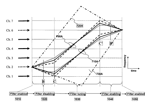
Fig. 7A shows a possible embodiment of the tuning technique in accordance to
the present invention. The reference sign 700A refers to three possible
alternative
trajectories (dotted, solid and dashed curves) of the resonance of interest of
one of the
two resonators and the reference sign 710A refers to three possible
alternative
trajectories of the resonance of interest of the other of the two resonators.
In particular,
dotted lines show an exemplary variant of the trajectory pattern.
Independently from the
symbol used (respectively dotted, solid and dashed), any combination obtained
by a
choice of one out of the three curves 700A and one out of the three curves
710A is
suitable to the invention. A choice in accordance with the same symbol
(respectively
dotted, solid and dashed) gives an exemplary maximum resonance separation
(during
massive tuning) equal to 1.5 times the channel spacing. Curves 720A and 730A
(dot-
dashed) show further possible alternative paths of the resonance curves
wherein the
massive filter tuning step 1030 may be considered absent. The main difference
with
CA 02703543 2010-04-23
WO 2008/055529 PCT/EP2006/010732
23
respect to the method described with reference to Fig. 4 is that now during
the step 1020
of filter disabling and the step 1040 of filter enabling, one of the two
resonators is tuned
so that the respective relevant resonance moves in the frequency spectrum
staying on
opposite sides with respect to, respectively, the initial frequency and the
final one. As a
consequence, any hit before the maximum resonance separation is reached (e.g.
any hit
during the enabling and the disabling steps) can be avoided, as long as the
maximum
resonance distance does not exceed the value of twice the channel frequency
spacing. In
Fig. 7A the hits occur solely during massive tuning step, in a total number of
six in
correspondence to the dotted and solid curves, which increases up to eight
hits (hitting
also channel 1 and 7) choosing both the dashed curves. Moreover, in case the
maximum
separation does exceed the double of the frequency spacing, the present
solution allows
avoiding any hit in correspondence to a resonance separation less than twice
the
frequency spacing. Due to the point symmetrical configuration of the patterns
shown in
Fig 7A, the overall power hit of the entire procedure is not affected by the
choice of
which one of the two rings (the one coupled closest to the input-to-thru
waveguide or
the other) corresponds to curve 700A or 710A. In particular, the resonator
whose
resonance of interest overshoots during disabling of the filter is different
from the
resonator whose resonance of interest overshoots during enabling of the
filter.
Fig. 7B shows an alternative embodiment of the tuning technique in accordance
to an embodiment of the present invention. While the disabling step is similar
to that
described in Fig. 4, the enabling step is now performed in accordance to the
technique
shown in Fig. 7A. Due to the asymmetry of the pattern of Fig. 7B, it is
important which
ring corresponds to which curve. In accordance to a preferred embodiment, it
is a ring
different from the one closest to the input-to-thru waveguide which overshoots
with
respect to the strict tuning range which starts from the initial frequency and
ends at the
final one. Curve 700B corresponds to a ring different from the one closest to
the input-
to-thru waveguide while curve 710B corresponds to the ring closest to the
input-to-thru
waveguide. Curves 700B' and 710B' show possible alternative paths of the
resonance
curves 700B and 710B, respectively. Curves 720B and 730B show further possible
alternative paths of the resonance curves, respectively, wherein the massive
filter tuning
step 1030 may be conventionally assumed as shown in the figure or it may be
considered absent. The patterns used for the enabling and disabling steps may
be
CA 02703543 2010-04-23
WO 2008/055529 PCT/EP2006/010732
24
mutually exchanged provided that care is taken to mutually exchange also the
roles of
the two rings. The main difference with respect to Fig. 7A is that now a hit
is tolerated
at a resonance separation less than two times the channel spacing (exemplarily
equal to
the channel spacing during filter disabling), provided that care is taken that
this hit is
caused by a ring distal with respect to the input-to-thru waveguide. For
example,
assuming a channel spacing equal to 100 GHz, the power hit due to the ring
distal from
the input-to-thru waveguide is equal to about 0.4 dB on channel 3 (state B of
Fig. 7B -
see Fig. 5C) and about 0.2 dB on channel 4 and 5. As regard to curve 710B
(assumed to
represent the ring closest to the input-to-thru waveguide) the hit during
massive tuning
on channel 3, 4 and 5 is equal to about 0.7 dB, including the hit in the state
C' on
channel 5. An advantage of the present embodiment is that the maximum
frequency
tuning range spanned by both the rings is lower than those shown in Fig. 7A
(respectively 4.5 times the channel spacing - for the distal ring - and from 5
to 6 times).
Fig. 7C shows two further alternative embodiments of the tuning technique in
accordance to the present invention. Curves 700C and 720C refer to the
resonator
closest to the input-to-thru waveguide and curves 710C and 730C are the
corresponding
trajectories respectively associated to the other resonator. Also in this case
the patterns
are asymmetric, with the same implications described above with reference to
Fig. 7B.
The main difference is that now, while the resonance of the distal resonator
overshoots
(exemplarily in the disabling step), the proximal resonator may remain
unperturbed
(curve 700C) or it may slightly 'overshoot' in the same direction of the
distal resonator
(curve 720C). Again, the pattern allows that the hit in state B and B' is
caused by the
distal ring and it is thus mitigated.
The present invention further contemplates any combination of the patterns
shown in Fig. 7A to 7C. It is noted that in all embodiments of Figs. 7A-C,
either during
enabling or during disabling the resonance of the ring distal from the input-
to-thru
waveguide is preferably moved in the opposite direction with respect to that
needed for
going from the initial frequency to the final one.
Fig. 8 illustratively shows the effects of the solution in accordance to the
present
invention, with the assumption that the channel spacing is equal to 100 GHz.
Curve
1410 represents either state B or state B' of Fig. 7A (dotted lines) and curve
1420
correspondingly represents respectively either state C or state C' of Fig. 7A
(dotted
CA 02703543 2010-04-23
WO 2008/055529 PCT/EP2006/010732
lines), with the 'proximal' ring overshoot (assuming that the massive tuning
takes place
in the positive frequency region). The thru channel +100 GHz away from the
channel at
zero frequency suffers a hit only in correspondence to a resonance separation
of about
one and half the channel spacing, in contrast to a possible hit in
correspondence to only
5 one channel spacing in absence of the overshoot.
Although the present invention has been disclosed and described by way of
some embodiments, it is apparent to those skilled in the art that several
modifications to
the described embodiments, as well as other embodiments of the present
invention are
possible without departing from the essential features thereof/the scope
thereof as
10 defined in the appended claims.