Note: Descriptions are shown in the official language in which they were submitted.
CA 02703571 2012-02-21
1
ELECTRICAL PATTERNS FOR BIOSENSOR AND METHOD OF MAKING
FIELD OF THE INVENTION
The present invention relates generally to the testing of body fluids for
concentration of
analytes and more particularly to an electrochemical biosensor for such
testing and a method
of making the same.
BACKGROUND
Test strips or biosensors are often used to measure the presence and/or
concentrations of
selected analytes in fluid test samples. For example, a variety of test strips
are used to measure
glucose concentrations in blood to monitor the blood sugar level of people
with diabetes.
These test strips include a reaction chamber into which a reagent composition
has been
deposited. Current trends in test strips require smaller test samples and
faster analysis times.
This provides a significant benefit to the patient, allowing the use of
smaller blood samples
that can be obtained from less sensitive areas of the body. Additionally,
regarding
measurement systems for blood glucose, for example, faster test times and more
accurate
results enable patients to better control their blood sugar level.
Electrochemical biosensors are well known and have been used to determine the
concentration of various analytes from biological samples, particularly from
blood. Examples
of such electrochemical biosensors are described in U.S. Pat. Nos. 5,413,690;
5,762,770;
5,798,031; 6,129,823 and published application US2005/0013731.
For example, US2005/0013731 discloses an electrochemical
biosensor having a covering layer overlying a base substrate. The base
substrate has an
electrical pattern having electrodes and a reagent layer thereon. The base
substrate and
covering layer define a sample receiving chamber that draws fluid sample
therein by capillary
action, whereupon the fluid sample reacts with the reagent in the chamber. A
voltage or
potential is controlled or applied across the electrodes, and the current
generated is measured
at one or more times and is then correlated to analyte concentration.
"Coulometric" and
"potentiometric" techniques are also known in which charge or potential,
respectively, instead
of current is measured and correlated to analyte concentration.
Various techniques are known in the art to form the electrical patterns in
electrochemical
biosensors. For instance, screen printing is a wet material technique that
generally allows
CA 02703571 2012-02-21
2
reliable formation of electrode structures and patterns having a gap width or
feature size of
approximately 75 m or greater.
Laser scribing usually employs a high power excimer laser, such as a krypton-
fluoride excimer
laser with an illumination wavelength of 248 nm, to etch or scribe individual
lines in a
conductive surface material and to provide insulating gaps between residual
conductive
material which forms electrodes and other desired components. The scribing is
accomplished
by moving the laser beam across the surface to be ablated, and such a
technique can be
undesirably time consuming if a complex electrical pattern is to be formed on
the surface.
Broad field laser ablation is a technique that has recently been employed to
manufacture
electrochemical biosensors having incredibly accurate and highly defined
electrical patterns
with additional functionalities that have hitherto been unavailable. Examples
of such
electrochemical biosensors can be found in U.S. Patent No. 7,073,246, U.S.
Patent Publication
Nos. 2005/0103624, 2006/0200981, and 2006/0200982.
Publication No. 2005/0103624 discloses a high degree of accuracy
and definition with which electrical patterns can be formed with laser
ablation. Similarly, U.S.
Patent Publication No. 2005/0023137
discloses biosensors with incredibly small and complex electrical patterns
that provide a large
footprint on the base substrate for other components, such as a display and
power supply,
among others. Other known techniques involving lasers include laser induced
forward
transfer, or LIFT, such as is disclosed in U.S. Patent Nos. 6,177,151 and
4,752,455, and
WO 2007/033079.
It would be desirable to further improve the electrical patterns and method of
making the
same in electrochemical biosensors.
SUMMARY OF THE INVENTION
The present invention provides a novel electrochemical biosensor and an
inventive method of
making the same. In particular, the present invention provides an inventive
biosensor that
includes multiple regions in which the electrical pattern is formed from
different electrically
conductive materials. The present invention also provides an inventive method
for mass
producing biosensors as just described. In one embodiment of this method,
first and second
different electrically conductive materials are deposited side by side on a
portion of an
electrically insulating base material, and a plurality of electrical patterns
is formed on the
portion of the base material. Each electrical pattern includes a first region
formed from the
CA 02703571 2010-04-23
WO 2009/056299 PCT/EP2008/009143
3
first electrically conductive material electrically connected to a second
region formed from the
second electrically conductive material. The electrically conductive materials
can be deposited
as layers on the base material and portions of the layers can be removed to
form the electrical
patterns, or, the electrical patterns can be formed by transferring the
conductive material in
the shape of the electrical pattern directly to the base material, such as by
a laser direct transfer
technique.
In one embodiment there is provided a biosensor for determining presence or
concentration
of an analyte in a fluid sample. The biosensor has a substrate having an
electrical pattern
formed thereon that includes a working electrode, a counter electrode, contact
pads, and
traces electrically connecting the working and counter electrodes to their
respective contact
pads. One or more of a spacing layer and a covering layer overlies and
cooperates with the
substrate to define a chamber for receiving a fluid sample. The inventive
biosensor includes a
first region in which the electrical pattern is formed of a first electrically
conductive material
and a second region in which the electrical pattern is formed of a second
electrically
conductive material. At least one of the traces includes a first section
located in the first region
electrically connected to a second section located in the second region, the
first and second
sections being comprised of the first and second electrically conductive
materials, respectively.
In particular embodiments, it is advantageous to provide the electrical
patterns of the first and
second regions in an overlapping arrangement, which is to say that part of the
electrical
pattern will overlap the other at the transition from region to region. At the
transition point,
the overlapped portion may be slightly thicker than the remainder of the
pattern. In other
embodiments, the transition from one region to another can be made by abutting
the
electrical patterns against one another at the transition, or by having one of
the regions
become gradually thinner across the transition while the other becomes
gradually thicker, the
net thickness over the transition remaining substantially the same. In yet
other embodiments
it may be desirable to form a seed layer to obtain a good connection between
overlapping
conductive materials, as described in more detail below.
Biosensors in accordance with these teachings typically comprise a generally
thin and flat
biosensor body having a length greater than its width, a dosing end where the
electrodes are
typically located, and a meter insertion end where the contact pads are
typically located. The
biosensor body has at least two regions in which the electrical pattern is
formed of different
electrically conductive materials. The dosing end is located in one of these
regions and the
CA 02703571 2010-04-23
WO 2009/056299 PCT/EP2008/009143
4
meter insertion end is located in the other. The traces thus typically span
the regions in order
to electrically connect each electrode with its respective contact pad.
For example, in many embodiments it is desirable to provide the electrical
features that are
located in the sample receiving chamber with very high-quality electrically
conductive
material which is also not negatively affected by the presence of biological
components and/or
the particular reagent chemistry present in the sample receiving chamber.
Noble metals such
as gold, platinum and palladium are suitable conductors for this purpose and
can therefore be
provided in the region of the biosensor that includes the sample receiving
chamber. On the
other hand, other regions of the biosensor which do not include the sample
receiving chamber
need not be provided with a material as expensive or as susceptible to
scratching and damage
as noble metals, and a substantially more robust conductive material may be
used in these
regions. For example, copper is a suitable material choice for the electrical
pattern in a region
extending from the meter insertion end of the biosensor toward the region
which includes
sample receiving chamber.
Similarly, in another embodiment, the region of the biosensor that includes
the contact pads
can be provided with a material such as indium oxide doped with tin oxide
(ITO), which has
been shown to have suitable electrical conductive properties, but is also
suitably robust in
order to be resistant to scratching. It should be appreciated that if a
contact pad on a biosensor
is scratched and degraded as it is inserted into the meter, the resistance of
the biosensor may
be affected and in turn the accuracy of the test result may be compromised.
Providing the
electrical pattern at the meter insertion end of the biosensor with ITO or
copper, for example,
as the conductive material addresses this problem.
Typically, the regions of the biosensor are positioned side by side along a
lengthwise direction
of the biosensor. For example, the portion of the electrical pattern located
at the meter
insertion end of the biosensor is formed from one electrically conductive
material, the portion
of the electrical pattern located at the dosing end is formed from a second
electrically
conductive material, and the region therebetween can be formed of yet a third
electrically
conductive material, if desired.
In another form thereof, these teachings provide inventive methods for mass
producing
electrical patterns that are used in biosensors like those just described. In
one such method, an
electrically insulating base material is provided. First and second different
electrically
conductive materials are deposited on a portion of the base material
substantially side by side
to one another. A plurality of electrical patterns is formed on the portion of
the base material,
CA 02703571 2010-04-23
WO 2009/056299 PCT/EP2008/009143
and each electrical pattern includes a first region formed from the first
electrically conductive
material electrically connected to a second region formed from the second
electrically
conductive material. The first region of the electrical pattern comprises at
least one electrical
feature, for example, an electrode.
5 In one exemplary embodiment, the depositing step comprises depositing a
layer of the first
electrically conductive material on the portion of the base material and
depositing a second
layer of the second electrically conductive material on the portion of the
base material
substantially side by side to and in electrical contact with the first layer.
In one exemplary
production method, this layered portion of base material can be rolled onto a
supply roll and
provided as a "production-ready" material to a manufacturing process. This
material is then
unrolled and portions of the first and second layers are removed to form the
electrical patterns
having two regions electrically connected to one another. In particular
embodiments, broad
field laser ablation is used to remove the conductive material to form the
electrical patterns.
Broad field laser ablation advantageously allows several complete electrical
patterns to be
formed in a single step, all at once, or in a succession of steps, as desired.
It also allows great
precision and detail in the electrical patterns formed thereby. However, many
other methods
for removing the conductive material can be used to form the electrical
patterns, such as
photo etching, plasma assisted chemical etching, laser scribing and many
others.
In another embodiment, multiple layers or "stripes" of material can be
deposited on the base
material, typically in the form of a repeating pattern. The base material can
then be divided or
cut into smaller portions of substantially identical production ready material
like just
described. This material can then be rolled up into rolls and sent to a
further production
station where the rolls will be unrolled, have portions of their conductive
layers removed to
form electrical patterns, and then further processed into finished biosensors.
Thus, depending
upon the particular requirements, the base material can be formed with as
little as only two
side by side layers of different conductive materials to a hundred or more
side by side layers,
typically in a repeating pattern.
In yet another embodiment, the inventive electrical patterns are formed
directly on the base
material by a technique such as laser induced forward transfer ("LIFT") or
similar techniques
known in the art. In such a technique, further removal of conductive materials
to form the
electrical patterns is unnecessary. Instead, the conductive material in the
shape of the desired
electrical pattern is transferred directly, typically from a laser transparent
substrate, to the base
material. In one embodiment incorporating this technique, a broad field laser
beam is
CA 02703571 2010-04-23
WO 2009/056299 PCT/EP2008/009143
6
projected through a mask having an opening in the shape of a portion of the
electrical pattern,
whereby a portion of the conductive material in the shape of the pattern is
removed from a
thin film of the same and transferred to the base material. Thus, in this
embodiment, the
electrical pattern or a portion thereof takes its shape before the transfer of
the conductive
material to the substrate is completed. A similar technique can be used to
directly transfer
additional regions of the electrical pattern to the base material.
Once the electrical patterns are formed on the portions of base material,
further processing
steps are utilized to complete the assembly of the biosensors. Typically, a
reagent is coated or
deposited on or over at least a portion of one or more of the electrodes of
the electrical
patterns, the reagent usually covering at least a portion of the working
electrode. A covering
layer and/or a spacing layer is then laminated over the portion of the base
material, thereby
forming a cover and defining a sample receiving chamber for each individual
biosensor to be
formed. Finally, cutting tools are used to cut through the covering layer,
spacing layer and the
base material to form individual biosensors in a mass production fashion. As
noted, the
electrical pattern of each individual biosensor will include at least two
regions in which the
material composition of the electrical patterns is different, the advantages
of which have been
noted above and will become more apparent below and in reference to the
attached Figures.
BRIEF DESCRIPTION OF THE DRAWINGS
The above-mentioned aspects of the present invention and the manner of
obtaining them will
become more apparent and the invention itself will be better understood by
reference to the
following description of the embodiments of the invention, taken in
conjunction with the
accompanying drawings, wherein:
Fig. 1 is a perspective view of a biosensor formed in accordance with these
teachings;
Fig. 2 is an exploded perspective view of the biosensor shown in Fig. 1;
Fig. 3 is a perspective view schematically illustrating the depositing of
multiple side by side
layers or films of conductive material on a base material;
Figs. 3A -3D are fragmentary side views showing various arrangements of the
transition region
between two side by side layers of different electrically conductive
materials;
Fig. 4 is a fragmentary perspective view illustrating the forming of
electrical patterns on a
portion of the base material of Fig. 3 to form a base substrate web;
CA 02703571 2010-04-23
WO 2009/056299 PCT/EP2008/009143
7
Fig. 5 is a perspective view of a biosensor base substrate web having a
reagent layer or stripe
applied thereto;
Figs. 6-9 are perspective views of various base materials from which the
electrical patterns of
multiple biosensors can be formed;
Fig. 1OA is a perspective view of a biosensor substrate having an electrical
pattern of three
different conductive materials formed thereon;
Fig. lOB is a perspective view of a biosensor substrate in accordance with an
alternate
embodiment;
Fig. 11 is a perspective view showing a roll of base material having two
conductive layers on it
and a laser scribing technique being used to form electrical patterns;
Fig. 12 is a perspective view schematically illustrating the production of an
alternate biosensor
embodiment employing these teachings;
Fig. 13 is a perspective view schematically illustrating an alternate
embodiment for producing
electrical patterns useful for biosensors according to these teachings; and
Fig. 14 is a perspective view schematically illustrating yet another alternate
embodiment for
producing electrical patterns useful for biosensors according to these
teachings.
The embodiments of the present invention described below are not intended to
be exhaustive
or to limit the invention to the precise forms disclosed in the following
detailed description.
Rather, the embodiments are chosen and described so that others skilled in the
art may
appreciate and understand the principles and practices of the present
invention.
Turning now to Figs. 1 and 2, there is shown an embodiment of a biosensor
useful in
accordance with the present teachings. Biosensor 20 includes a base substrate
22, a spacing
layer 24 and a covering layer comprising body cover 28 and chamber cover 30.
The spacing
layer 24 includes a void portion 32 to provide a sample-receiving chamber 34
extending
between the base substrate 22 and the covering layer. An alternative covering
layer could
comprise a top cover (not shown) overlying the spacing layer 24 and including
a vent hole
(not shown) in fluid communication with the sample-receiving chamber 34.
The base substrate 22 carries an electrical pattern 36 including a plurality
of electrodes 38
including at least a working electrode 39 and counter electrode 37. Electrical
pattern 36 also
CA 02703571 2010-04-23
WO 2009/056299 PCT/EP2008/009143
8
includes electrode traces 40 terminating in contact pads 42. The electrodes 38
are positioned
within the sample-receiving chamber 34. In one embodiment, electrodes 38
include separate
working and counter electrodes 50, 51 for detecting dosing sufficiency before
a measurement
sequence can begin. As described in more detail below, e.g., with reference to
Figs. 11 and 12,
various other configurations of electrical patterns may be formed in
accordance with these
teachings, depending upon the particular electrical features desired for the
biosensor. A
suitable reagent system 43 (Fig. 2) overlies at least a portion of one of the
electrodes,
particularly the working electrode, and is shown in Fig. 2 overlying
electrodes 37, 39, and a
portion of electrodes 50 and 51 within the sample-receiving chamber.
The body cover 28 and the chamber cover 30 overlying the spacing layer 24 have
a gap 44
therebetween, which defines a vent opening communicating with the sample-
receiving
chamber 34 to allow air to escape the chamber as a sample fluid enters the
chamber from the
edge opening or fluid receiving opening 45 (Fig. 1). Biosensor 20 includes a
dosing end 46 and
a meter insertion end 48. The dosing end is typically distinguishable from the
meter insertion
end so as to aid users. For example, the biosensor of Fig. 1 has a beveled
dosing end 46, and it
provides a color contrast between the dosing end and the remainder of the
biosensor, e. g. by
coloring a portion 33 of the spacer layer 24 at the dosing end. One or both of
these are
sufficient examples of how to distinguish the dosing end from the meter
insertion end. In
addition, strip graphics can be used to further improve the intuitiveness of
the strip design;
e.g., arrow 41 indicates the direction of insertion of the strip into the
meter.
Turning now to Fig. 2 in particular, the biosensor includes a base substrate
22 which
comprises an insulating material supporting the electrical pattern 36 and
other components of
a biosensor. Typically, plastics such as vinyl polymers, polyimides,
polyesters, and styrenes
provide the electrically insulating and structural properties which are
required. Further, for
embodiments of a biosensor 20 according to the present teachings that are mass
producible
from rolls of material, as discussed in greater detail below, it is desirable
that the material
properties be appropriate to have sufficient flexibility for roll processing,
while also giving a
useful stiffness to the finished biosensor. The insulating material of base
substrate 22 can be
selected as a flexible polymeric material such as polyester, especially high
temperature
polyester materials; polyethylene naphthalate (PEN); and polyimide, or
mixtures of two or
more of these. Polyimides are available commercially, for example under the
trade name
Kapton , from E.I. duPont de Nemours and Company of Wilmington, Del. (duPont).
A
particularly suitable base substrate insulating material is MELINEX 329
available from
duPont.
CA 02703571 2010-04-23
WO 2009/056299 PCT/EP2008/009143
9
The electrodes 38, e.g., at least the measuring electrodes comprising a
working electrode 39
and a counter electrode 37, are at least partially exposed within the sample-
receiving chamber
34. The sample-receiving chamber is configured such that sample fluid entering
the chamber
is placed in electrolytic contact with both the working electrode 39 and the
counter electrode
37. This allows electrical current to flow between the measuring electrodes 38
upon the
electrooxidation or electroreduction of the analyte resulting from an
electrical potential or
voltage being applied or controlled between the electrodes 38.
These teachings disclose a biosensor having two or more regions in which the
electrical
pattern 36 is formed from different conductive materials. For example, Fig. 2
shows two
general regions 70 and 72. In one embodiment, the electrical pattern 36 in
region 70, which
includes electrical features such as electrodes 38 (e.g., working and counter
electrodes 37, 39
and dose sufficiency electrodes 50, 51) and at least a portion of one or more
of the electrode
traces 40, can be formed from a noble metal such as gold, silver, palladium,
or platinum, as is
indicated by a light shade of gray illustrated in Fig. 2. For typical
embodiments comprising an
analyte biosensor, since region 70 contains the reagent that reacts with the
fluid sample when
the biosensor is dosed and the electrochemical reaction occurs there, this
region in certain
embodiments is formed with a sensitive, premium conductive material such as a
noble metal.
On the other hand, the remainder of the electrical pattern 36 comprising
region 72 may not
require a premium conductor in certain embodiments. Thus, a more robust
material such as
copper, indium-tin oxide, or carbon ink, may form the electrical pattern in
region 72 in the
embodiment illustrated in Fig. 2. As will become more apparent with reference
to the
description of the method of production presented below, this disclosure
teaches a wide
variety of options for forming two or more regions in a biosensor, each region
having different
electrically conductive material in the electrical pattern. The selection of
the material for each
region typically depends on the specifications and/or uses for the biosensor,
and may be
optimized as needed or desired, according to the knowledge and skill of a
person of ordinary
skill in the art. The transition between regions typically occurs in the
traces, such that each
trace has one segment or section formed from the conductive material of one
region and a
second segment or section formed from the conductive material of the other
region.
Turning now to Fig. 3, one exemplary method of mass producing the electrical
patterns 36 for
electrochemical biosensors can be appreciated. In this exemplary embodiment, a
flexible and
substantially flat base material 80 is provided on a supply roll 82. Base
material 80 on roll 82
has been pretreated as desired to clean or modify the surface 83 and make it
ready to receive
CA 02703571 2010-04-23
WO 2009/056299 PCT/EP2008/009143
conductive layers, as is known in the art. As material 80 is unrolled, it
passes through
successive processing stations 84, 86, 88 and 90 shown schematically in Fig.
3. In these
processing stations thin films or layers of conductive material are deposited
or applied side by
side, but may be allowed to overlap to a certain extent. The extent to which
the layers are
5 offset or overlap, if at all, can be varied depending upon the particular
application and/or
desired electrical specifications or effects. In one embodiment, the degree of
overlap or offset
is maintained substantially uniform along the entire length of the insulating
material 80 in
order to, as will be appreciated from the description below, form biosensors
substantially
identically with respect to electrical properties within the roll and from
roll to roll.
10 In the illustrated embodiment of Fig. 3, for example, at station 84, a thin
conductive film or
layer 92 is shown being deposited on surface 83. At station 86, a layer or
film 94 of a
conductive material different from layer 92 is deposited adjacent to layer 92
such that layer 94
overlaps layer 92 as indicated by dashed line 96. At stations 88 and 90,
layers 98 and 100 are
deposited in the same manner as layers 92 and 94, respectively. Further, in
this embodiment,
layers 92 and 94 are the same width as layers 98 and 100, respectively, the
advantages of which
will become apparent. In this embodiment, layer 98 is applied such that there
is minimal if any
overlap with layer 94. This is because once it has passed the processing
stations 84, 86, 88, 90,
the base material 80 is cut with knife 102 as shown to form two identical
smaller portions 104
and 106 each comprising a production-ready base material, which are rolled
onto two take-up
spools, one of which is illustrated in Fig. 3 at reference numeral 108. There
need be no
electrical conductivity between layers 94 and 98 since they are ultimately
separated by cutting,
and overlap of these layers is therefore unnecessary. Layers 92 and 100 may be
applied to the
opposite lateral edges, respectively, of surface 83 or may be applied such
that a small band of
uncovered material remains at the edges as shown. Further trimming may or may
not be
necessary depending on the particular biosensor design.
It should be understood that the "stations" shown in Fig. 3 can represent any
of a wide variety
of techniques for applying the conductive layers. Examples of suitable
techniques include but
are not limited to sputtering, physical vapor deposition (PVD), plasma
assisted chemical
vapor deposition (PACVD), chemical vapor deposition (CVD), electron beam
physical vapor
deposition (EBPVD), and/or metal-organic chemical vapor deposition (MOCVD).
Vapor
deposition is typically performed under vacuum. These techniques are well
known in the art
and can be used to selectively provide uniformly thin coatings of metal or
other conductive
materials onto a substrate as depicted in Fig. 3. The resulting base material
can be inspected to
ensure that the conductive coatings or layers are uniform and free of material
defects.
CA 02703571 2012-02-21
11
Further, while the stations 84-90 are shown set up one after the other in Fig.
3, one of skill in
the art would readily recognize many variations for forming the conductive
layers. For
example, the conductive material depositing stations can be positioned in
about the same
location and the roll 82 indexed back and forth. During each pass a different
conductive layer
would be applied. Other variations are possible.
As suggested above, many conductive materials can be used for the layers shown
in Fig. 3,
depending upon the particular application for the biosensor. The conductive
layers may
contain pure metals, alloys, or other conductive materials such as carbon inks
and the like.
Examples of suitable conductors include: aluminum, carbon (such as graphite),
cobalt,
copper, gallium, gold, indium, iridium, iron, lead, magnesium, mercury (as an
amalgam),
nickel, niobium, osmium, palladium, platinum, rhenium, rhodium, selenium,
silicon (such as
highly doped polycrystalline silicon), silver, tantalum, tin, titanium,
tungsten, uranium,
vanadium, zinc, zirconium, mixtures thereof, and alloys or solid solutions of
these materials.
Indium tin oxide (ITO) is a conductor material which can be used on the meter
insertion end
of the biosensor, as described in more detail below. In other embodiments,
materials can be
selected to be essentially unreactive to biological systems; such materials
include: gold,
platinum, palladium, iridium, or alloys of these metals. The conductive layer
may be any
desired thickness.
Further, one of skill in the art would recognize that certain selected
combinations of
conductive materials for adjacent regions may require a so-called "seed layer"
to ensure good
physical adherence and structural and chemical stability between the two
layers at the
transition between regions, i.e., where the layers either abut or overlap. For
example, if the two
regions are formed from copper and gold, respectively, one approach would be
to first deposit
the copper layer on the base material, then apply a seed layer of, e.g.,
chromium, titanium
nitride or aluminum nitride on the copper at the location where the gold layer
will abut or
overlap the copper, and then apply the gold layer. The use of seed layers is
known in the art
and examples of the same are disclosed in U.S. Patent No. 6,822,176.
If an overlapping arrangement is employed, it is envisioned that the width of
the overlap need
only be a few millimeters, e.g., from Ito 3 mm, typically on the order of
about 2 mm. In
embodiments in which an overlapping arrangement is employed, it is generally
desirable to
provide sufficient overlap to ensure that the layers are continuously
connected along their
length despite deviations in layer width due to manufacturing limitations. Of
course, the
CA 02703571 2012-02-21
12
electrical pattern may be thicker in the region of any such overlap. Fig. 3A,
for example,
illustrates an overlap region or transition 97 of conductive layers 92 and 94
in which the
arrangement of layers is thicker in the overlap region 97. As discussed above,
the layers can
also be formed in an abutting relationship as illustrated in Fig. 3B, in which
layers 92 and 94
abut one another as shown at reference numeral 99. It may be desirable in some
circumstances
to include an additional conductive seam layer 101 (shown in phantom in Fig.
3B) to allow for
possible gaps between the two layers arising from manufacturing limitations in
forming an
abutting joint.
One of skill in the art would recognize other means for electrically
connecting the adjacent
conductive layers. For example, the deposition technique may be such that one
layer becomes
thinner while the other becomes thicker traversing the region of overlap, such
that the overall
thickness over the transition between the two regions remains roughly the
same, e.g., as shown
at reference numeral 103 in Fig. 3C. Stated another way, the deposition
technique used to
form the transition shown in Fig. 3C is one in which both layers are thinner
at their edges. It is
also possible to form the layers spaced apart initially and then electrically
join them by
applying a third conductive material between them, e.g., as shown in Fig. 3D,
in which the
conductive seam layer 105 joins layers 92 and 94. This approach may prove
especially useful
when it is desired to electrically connect two conductive material layers that
are not physically
or chemically compatible when directly contacting one another, as discussed
above with
regard to seed layers. One of skill in the art would recognize from this
disclosure various other
possibilities for forming the transition between the two conductive regions,
all of which are
considered within the spirit and scope of this disclosure.
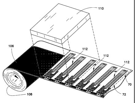
Turning now to Fig. 4, the production-ready base material 106 formed as shown
in Fig. 3 is
now unwound in a different process stage and advanced through a laser ablation
apparatus
110 shown diagrammatically in Fig. 4. A laser apparatus and process suitable
with these
teachings is described in U.S. Patent No. 7,073,246 and U.S. Publication No.
2005/0103624,
referred to above. In exemplary embodiments, the laser apparatus performs
broad field laser ablation with a sufficiently large projection to ablate the
conductive material
in order to form several electrical patterns 112 in a single step. In the
particular example
illustrated in Fig. 4, base material 106 is indexed such that three electrical
patterns are formed
in a single step by removing portions of the conductive material from the base
material except
where the electrical patterns are to be defined. As shown, conductive material
is removed such
that two regions 70 and 72 of each electrical pattern 112 having different
electrically
CA 02703571 2012-02-21
13
conductive material are formed. The resulting structure is a base substrate
web 107 (Fig. 5)
that can be further processed for purposes of manufacturing a plurality of
biosensors.
In one embodiment, the base substrate web 107 is further processed by adding a
layer 114 of
reagent material as shown in Fig. 5. Suitable compositions for reagent layer
114 and the
S method of applying it are disclosed in U.S. Publication No. 2005/0016844,
and need not be repeated in detail herein. Briefly, the
reagent layer may be applied by any number of suitable dispensing techniques
such as curtain
coating, hot melt coating, rotary screen coating, doctor blade or air knife
coating, Meyer bar
coating, and reverse roll coating techniques. The reagent layer 114 is
typically deposited on the
base substrate web 107 as a wet composition at a thickness of between about 50
m and about
100 m. In the embodiment shown in Fig. 5, to ensure that the reagent layer
114 only contacts
the conductive material in region 70 (which may be a noble metal), and to
allow for
manufacturing tolerances in the application of layer 114, a portion 120 of
region 70 may
extend beyond or protrude from under the reagent layer 114 as shown. After the
reagent layer
is applied, the various other layers, such as spacing layer 24 and the
covering layer are
assembled, typically with roll processing techniques as described in U.S.
Publication No.
2005/0016844 to form completed biosensors such as are illustrated in Figs. 1
and 2.
It should be readily recognized that many variations for forming and cutting
the base material
into the smaller, production-ready base materials, if desired, as well as the
number, location
and material composition of the different regions of electrical patterns on
the biosensors
themselves are possible.
For example, Fig. 6 illustrates one embodiment in which the base material 600
can be formed
with only two electrically conductive layers 602 and 604 positioned
substantially side by side
and in electrical communication with one another. Base material 600 can be
formed as
described above with reference to Fig. 3 with only two processing stations or
passes, and then
be provided directly to a production process much like that discussed above
with respect to
Fig. 4 for forming the base substrate web 107 without cutting beforehand. That
is, base
material 600 is initially provided as a production-ready base material, in
contrast to the base
material 80 of Fig. 3 which is cut down into production-ready lots of base
material 104, 106.
Alternatively, Fig. 7 shows a base material 700 having 3 conductive layers
702, 704 and 706
formed thereon by, e.g., a process similar to that shown and described with
reference to the
description of Fig. 3. Layers 702 and 706 are comprised of the same
electrically conductive
material and layer 704 is formed of a different electrically conductive
material that can be cut
CA 02703571 2010-04-23
WO 2009/056299 PCT/EP2008/009143
14
along dashed line 708 to form two identical production-ready lots of base
material. Such an
arrangement essentially allows two layers to be formed in a single step (i.e.,
layer 704 is divided
in half and ultimately becomes two layers in different production lines) and
thus provides
certain efficiencies.
Fig. 8 illustrates a multilayer base material 800 having repeating layers or
"stripes." Layers 802,
806 and 810 are formed of the same conductive material and have substantially
the same
width. Layers 804, 808 and 812 are also all formed of the same conductive
material (different
than layers 802, 806, and 810) and have substantially the same width. Three
lots of
production-ready base material can thus be formed by making two cuts along
lines 814 and
816, respectively.
Fig. 9 shows a base material 900 having five conductive layers 902, 904, 906,
910 and 912
formed thereon by, e.g., a process similar to that shown with reference to the
description of
Fig. 3. Layers 902 and 912 are comprised of the same electrically conductive
material and
layers 904 and 910 are comprised of the same electrically conductive material,
different than
layers 902 and 912. Layer 906 is formed of a third different electrically
conductive material.
The base material 900 can be cut along dashed line 914 to form two identical
lots of
production-ready base material, each having three layers or stripes extending
substantially side
by side.
It should be readily recognized from these teachings that that the number of
repeating layers
or stripes and their configuration on the base material (before it is cut into
production-ready
lots, if needed) can be varied as desired as a function of manufacturing
efficiency and the
desired number and type of regions in the electrical pattern of the biosensors
to be formed.
For example, it is envisioned that base materials useful in large scale
production using these
teachings could be as wide as 1.5 m or more and include 100 or more side by
side layers or
stripes. Many cuts would obviously then be made to this striped base material
to reduce it into
multiple lots of production-ready base material that would be further
processed.
With reference to Fig. 10A, a biosensor base substrate 1000 is shown formed
from a base
substrate web formed from one of the portions of base material formed as
described with
reference to Fig. 9. The base substrate 1000 has three regions 1002, 1004 and
1006 in which the
electrical pattern comprises a different conductive material. However, it
should be recognized
that embodiments in which three or more electrical pattern regions are
provided, it may be
desirable to have some regions with the same conductive material. For example,
in a biosensor
comprising a base substrate configured like base substrate 1000, it may be
desirable to have the
CA 02703571 2012-02-21
regions 1002, 1006 at the two ends formed of the same material and the middle
region 1004
formed of a different material. While a virtually endless variety of material
compositions could
be employed for a base substrate 1000 having an electrical pattern comprising
three regions,
one exemplary embodiment would include region 1002 formed of a noble metal
such as gold
5 or platinum, region 1004 formed of a good conductor such as copper, and
region 1006 formed
of a robust material that is resistant to scratching (e.g., when the completed
biosensor is
inserted into a meter) such as ITO.
It should also be understood that, while the electrical patterns and their
formation described
above have been rather sophisticated, these teachings can advantageously be
employed for a
10 wide variety of electrical patterns that are employed in biosensors. For
example, Fig. 10B
illustrates a biosensor base substrate 1020 having two regions 1022 and 1024
in which the
conductive tracks 1026 and 1028 of the electrical pattern comprise different
conductive
materials. This embodiment illustrates that the electrical patterns for which
these teachings
can be utilized can be quite simple, in this case comprising merely two
conductive tracks. The
15 base substrate 1020 forms part of a "side fill" biosensor having a
capillary chamber in the area
shown by dashed line.1030. A vent hole 1032 for the capillary chamber and a
notch 1034 is
provided to aid in filling the chamber with sample fluid. Aside from the
regions of the
electrical pattern formed from different conductive materials, such a
biosensor is known in
the art and an example of the same can be found in U.S. Patent No. 6,270,637.
Fig. 11 illustrates yet another of the simpler designs in which these
teachings can be employed.
In this embodiment, base material 1106 on roll 1108 is shown being unwound for
forming a
base substrate web comprising a plurality of rudimentary electrical patterns
formed by laser
scribing. In this embodiment, a laser apparatus 1110 projects a beam 1112 as
apparatus 1110 is
moved along the path indicated by dashed lines 1114. In so doing, multiple
electrical patterns
each comprising, e.g., counter electrode 1116, working electrode 1118, and
traces 1120, 1122,
are formed, the traces comprising electrical contacts at the ends opposite the
electrodes.
Separate base substrates to be assembled into individual biosensors, e.g., as
described above,
can be formed by cutting along dashed lines 1124. Instead of laser apparatus
1110, one of skill
in the art would readily recognize other suitable means for removing the
conductive material
to form the electrical patterns, such as etching, mechanical removal of the
conductive material
and many others.
CA 02703571 2012-02-21
16
One of skill in the art could also readily employ these teachings to form
electrical patterns in
multiple layers of a biosensor such as are found in biosensors having so-
called "facing
electrodes." For example, Fig. 12 shows a first roll 1201 of base substrate
web 1202 having a
series of working electrodes 1204 of one electrically conductive material and
traces 1206 of a
different electrically conductive material formed at spaced intervals thereon,
which can be
formed by the methods described herein. The ends of the traces comprise
electrical contacts
for meter insertion, as described elsewhere herein. Similarly, a second base
substrate web 1208
is provided on roll 1209 and includes a series of counter electrodes 1210 made
of one
electrically conductive material and traces 1212 of a different electrically
conductive material
formed at spaced intervals thereon. Electrodes 1204 and 1210 can be formed of
the same or
different materials, as can traces 1206 and 1212.
In the embodiment illustrated in Fig. 12, two middle layers 1218 and 1219 of
an electrically
insulating material are provided on rolls 1220 and 1221, respectively. Rolls
1220 and 1221 are
arranged during processing (unrolling) such that a gap 1226 that is defined
between edges
1234 and 1236 is maintained. These middle layers form spacing layers in the
biosensors
produced and also define the capillary sample receiving chamber for the
biosensors. Middle
layer 1218 includes a plurality of rectangular notches 1228 formed in it that
ultimately define
openings 1230 in the biosensors produced to allow access by the electronics of
a meter to
electrical traces 1206 and 1212.
During production, the top and bottom webs 1208 and 1202, respectively, are
laminated
together and sandwich middle layers 1218 and 1219 therebetween to form the
precursor or
laminate structure 1222. Precursor 1222 includes a top layer formed from
material 1208
having the counter electrodes 1210 formed on its underside, two side by side
spaced middle
insulating layers formed from material 1218 and 1219, and a bottom layer
formed from
material 1202 having the working electrodes 1204 formed on its top side.
Examples of roll
processing techniques that are used to form such a laminate structure can be
found in U.S.
Publication No. 2005/0016844.
The precursor 1222 includes a series of openings 1230 that are defined by
notches 1228 of
layer 1218. The ends or contact portions of traces 1206 can be seen in the
openings 1230 of
laminate structure 1222. Edges 1234 and 1236 are shown in phantom in the
precursor 1222,
and gap 1226 forms a rectangular passageway 1232 with a series of working
electrodes 1204
and counter electrodes 1210 spaced along its length and facing one another.
The completed
biosensors with "facing electrodes" are formed by cutting along dashed lines
1224. Each
CA 02703571 2012-02-21
17
biosensor so formed will have sample receiving openings formed on both sides
thereof and an
access opening 1230, as is known in the art.
Of course, in some circumstances it may be desirable to form only one of the
facing electrodes
(or other electrical feature) from more than one electrically conductive
material. For example,
in the embodiment of Fig. 12, it may be desirable to form counter electrodes
1210 and traces
1212 of the same material. Generally, when these teachings are employed in
facing electrode
arrangements, at least one of the base substrate webs will have an electrical
pattern with at
least two regions of different electrically conductive material, and the two
webs are combined
into a laminate such as laminate 1222 with electrical patterns and/or
electrical features
arranged facing one another.
From the above teachings, one of skill in the art will appreciate that the
electrical patterns and
formation thereof described above can be employed in a wide variety of
biosensor designs,
ranging from biosensors having the most rudimentary electrical patterns, to
those having
highly sophisticated patterns providing multiple electrical functionalities,
to those having
electrical patterns or electrical features on multiple substrates, among
others. Additionally,
these teachings are not limited to depositing conductive layers on a base
material and then
removing portions of the conductive layers to form the electrical patterns.
Instead, electrical patterns having multiple regions could be directly
deposited onto a base
material to form a base substrate web without requiring further removal of
conductive
material from the base material to complete the electrical patterns. For
example, in a
technique such as "laser induced forward transfer" ("LIFT"), a pulsed laser
beam is directed
through a laser-transparent target substrate to strike a film of material
coated on the opposite
side of the target substrate. The laser vaporizes the film and, due to the
transfer of momentum,
the material is removed from the target substrate and is deposited on a
receiving substrate that
is placed in close proximity to the target substrate. This LIFT process
obviously transpires
quite rapidly, but it can be appreciated that the forming of the conductive
material into the
shape of the electrical patterns or portions thereof is at least initiated
before transfer of the
conductive material to the substrate is completed. Various methods for
carrying out LIFT and
similar techniques are disclosed in U.S. Patent Nos. 6,177,151; 4,752,455;
5,725,706; 5,292,559;
5,492,861; 5,725,914; 5,736,464; 4,970,196 and 5,173,441.
Turning to Fig. 13, two rolls 1302 and 1304 of different electrically
conductive materials 1306
and 1308, respectively, are provided. Each roll has a top flexible layer 1310
and 1312,
CA 02703571 2010-04-23
WO 2009/056299 PCT/EP2008/009143
18
respectively, of laser transparent material to which the conductive materials
1306 and 1308 are
adhered or otherwise coated or deposited, as described in the references
incorporated above.
Flexible laser-transparent layers 1310 and 1312 suitable for roll processing
can be made from,
e.g., polyethylene, polypropylene, polyvinyl acetate, polystyrene,
polyethylene terephthalate,
polybutylene terephthalate, and polytetrafluoroethylene, among others.
As illustrated in Fig. 13, the region 1328 of the electrical pattern that
includes the working
electrodes 1320 and counter electrodes 1322 is formed by projecting a broad
field laser beam
1324 from laser apparatus 1325 through mask 1326, which results in first
region 1328 of the
electrical pattern being deposited on the base material 1330 as shown.
Meanwhile, the same
technique is used to form the second region 1332 of the electrical pattern
downstream along
base material 1330. That is, a broad field laser beam 1338 is projected from
laser apparatus
1340 through mask 1341, which results in the second region 1332 of the
electrical pattern
having traces 1350 and contact pads 1352 being deposited on the base material
1330 as shown.
Multiple electrical patterns are formed in this manner by coordinating the
unwinding and
indexing of rolls 1302, 1304 and 1342, which have take-up spools 1344, 1346
and 1348,
respectively. The take-up spool 1348 of base material 1330 having electrical
patterns thereon
comprises the base substrate web that can be further processed to make
biosensors through
further roll processing and lamination techniques as described above.
As noted above, depending upon the particular conductive materials chosen for
regions 1328
and 1332, it may be necessary to deposit a seed layer over region 1328 before
depositing region
1332 of the electrical pattern. Such a seed layer in the form of a partial
electrical pattern can be
deposited by the same LIFT technique used to deposit regions 1328 and 1332.
Similar to the
layer approach described with reference to Figs. 3-9, regions 1328 and 1332
can be formed
spaced apart, and a connecting layer in the form of a partial pattern can be
deposited
therebetween. It may, e.g., be desirable to form the transition between the
regions of the
electrical pattern at a location where the pattern is least complicated, which
may allow greater
tolerances in the indexing and flexibility in the exact location at which the
partial patterns
must be deposited to sufficiently align.
While some laser direct write transfer techniques transfer a material from a
laser transparent
substrate, such is not necessary. For example, U.S. Pat. No. 4,895,735 to Cook
("the `735
patent") discloses a technique in which the conductive material is held above
the substrate and
a laser is used to deposit the conductive material in a pattern. Unlike the
art discussed above,
the conductive material is directly deposited without using a laser
transparent substrate to
CA 02703571 2010-04-23
WO 2009/056299 PCT/EP2008/009143
19
which the conductive layer is adhered. These teachings can be used to
incorporate such as
process, as is illustrated with respect to Fig. 14.
As shown in Fig. 14, two layers or films of different electrically conductive
material 1406 and
1408 are placed directly above a base material 1430 that is provided in roll
1442. In order to
minimize displacement of the layers 1406 and 1408, they may be fixed in place
or laid on top
of the base material 1430, as described in the `735 patent. As illustrated,
the region 1428 of the
electrical pattern that includes the working electrodes 1420 and counter
electrodes 1422 is
formed by projecting a broad field laser beam 1424 from laser apparatus 1425
through mask
1426, which results in first region 1428 of the electrical pattern being
deposited on the base
material 1430, as shown.
Meanwhile, the same technique of directly depositing a portion of the
electrical pattern to the
base material is used to form the second region 1432 of the electrical
patterns downstream
along material 1430. That is, a broad field laser beam 1438 is projected from
laser apparatus
1440 through mask 1441, which results in the second region 1432 of the
electrical pattern
having traces 1450 and contact pads 1452 being deposited on the base material
1430 as shown.
Multiple electrical patterns are formed in this manner by coordinating the
unwinding and
movement of the base material, the films, and/or laser apparatus, as desired.
The take-up
spool 1448 of base material 1430 having electrical patterns thereon comprises
the base
substrate web that can be further processed to make biosensors through further
roll processing
and lamination techniques as described above.
In addition to depositing the electrical pattern directly to the base material
as was just
described with reference to Figs. 13 and 14, a broad laser pulse could be used
to deposit an
entire section or layer of material, thereby producing a base material having
layers like those
depicted in, e.g., Figs. 3 and 6. Thereafter, laser ablation or other
techniques described above
can be used to remove a portion of the conductive materials to form the base
substrate web
having a plurality of electrical patterns each having multiple regions. One of
skill in the art
would readily recognize other variants for employing these teachings.
Regardless of the manner in which each conductive material layer is ultimately
deposited on
the base material, e.g., as a broad conductive layer or as a fully defined
electrical feature, it will
be appreciated from this disclosure that in an exemplary embodiment of the
present
invention, the first region typically comprises an electrode region having one
or more
electrically isolated electrodes, and the second region typically comprises a
contact region
comprising one or more electrically isolated contact areas, such as contact
pads, wherein the
CA 02703571 2012-02-21
electrode region and the contact region are electrically connected and are
respectively
comprised of the first and second different electrically conductive materials.
As described
above, the electrode region may be formed directly by a LIFT technique or by
depositing the
first electrically conductive material on the base material and removing at
least a portion to
5 define the desired electrical features for the electrode region. Similarly,
the contact region may
be formed directly by a LIFT technique or by depositing the second
electrically conductive
material on the base material and removing at least a portion to define the
desired electrical
features for the contact region. As also discussed above, the transition
between the electrode
and contact regions typically is located in the traces connecting these
regions. In this case, each
10 trace has one section formed of the first electrically conductive material
connected to the
electrode region and a second section formed of the second electrically
conductive material
connected to the contact region.
20 The following is a list of preferred embodiments of the invention:
1. A method of manufacturing a base substrate having an electrical pattern
thereon for
use in an electrochemical biosensor, the method comprising:
providing a base material having a first layer of a first electrically
conductive material
positioned substantially side by side to and in electrical contact with a
second layer of a second
electrically conductive material; and
removing at least a portion of the first layer and the second layer to form an
electrical
pattern on the base material, the electrical pattern including a first region
formed from the
first electrically conductive material electrically connected to a second
region formed from the
second electrically conductive material, the first region of the electrical
pattern comprising at
least one electrode.
2. The method of preferred embodiment 1, wherein the removing step comprises
ablating the portion of the first layer and the second layer by projecting an
image of the
CA 02703571 2010-04-23
WO 2009/056299 PCT/EP2008/009143
21
electrical pattern onto the base material with a laser apparatus to form the
electrical pattern
from both the first and second layers.
3. The method of preferred embodiment 1, further comprising repeating the
removing
step a plurality of times at spaced intervals along the base material to form
a base substrate
web having a plurality of the electrical patterns thereon.
4. The method of preferred embodiment 3, further comprising:
depositing a reagent layer on the base substrate web over at least a portion
of the at
least one electrode of each electrical pattern of the plurality of electrical
patterns;
laminating at least one covering layer or a spacing layer over the base
substrate web,
thereby forming covers and sample receiving chambers for individual biosensors
to be
formed; and
cutting through the at least one covering layer or spacing layer and the base
substrate
web to form a plurality of biosensors.
5. The method of preferred embodiment 1, wherein the removing step comprises
forming working and counter electrodes from the first electrically conductive
material and
forming contact pads from the second electrically conductive material.
6. The method of preferred embodiment 1, wherein the providing step comprises
providing the base material with the first layer formed from a noble metal and
the second
layer formed from an electrically conductive material substantially more
robust than a noble
metal.
7. The method of preferred embodiment 6, wherein the noble metal is selected
from the
group consisting of gold, silver, palladium and platinum.
8. The method of preferred embodiment 6, wherein the electrically conductive
material
for the second layer is selected from the group consisting of aluminum,
carbon, cobalt,
copper, gallium, indium, iridium, iron, lead, magnesium, mercury, nickel,
niobium, osmium,
rhenium, rhodium, selenium, silicon, tantalum, tin, titanium, tungsten,
uranium, vanadium,
zinc, zirconium, indium tin oxide and mixtures thereof.
9. The method of preferred embodiment 1, wherein the providing step comprises
providing the base material with the first and second layers in a partially
overlapping
arrangement.
CA 02703571 2010-04-23
WO 2009/056299 PCT/EP2008/009143
22
10. The method of preferred embodiment 1, further comprising, prior to the
providing
step, depositing the first and second layers of electrically conductive
material substantially side
by side along a portion of the base material.
11. The method of preferred embodiment 10, further comprising:
prior to the providing step, depositing third and fourth layers of
electrically conductive
material substantially side by side along a second portion of the base
material, the third layer
being adjacent to the second electrically conductive layer; and
cutting the base material between the second and third layers.
12. The method of preferred embodiment 10, wherein the depositing step
comprises one
or more of sputtering, physical vapor deposition, plasma assisted chemical
vapor deposition,
chemical vapor deposition, electron beam physical vapor deposition, metal-
organic chemical
vapor deposition, and laser induced forward transfer.
13. The method of preferred embodiment 1, further comprising providing a
second base
material having a second electrical pattern formed thereon and combining the
first base
material and the second base material into a laminate in which the first
electrical pattern faces
the second electrical pattern.
14. A method of manufacturing a base substrate web comprising a plurality of
electrical
patterns for use in electrochemical biosensors, the method comprising:
providing an electrically insulating base material;
depositing first and second different electrically conductive materials on a
portion of
the base material substantially side by side to one another; and
forming a plurality of electrical patterns on the portion of the base
material, each
electrical pattern including a first region formed from the first electrically
conductive material
electrically connected to a second region formed from the second electrically
conductive
material, the first region of the electrical pattern comprising at least one
electrical feature.
15. The method of preferred embodiment 14, wherein the depositing step
comprises
depositing a first layer of the first electrically conductive material on the
portion of the base
material and depositing a second layer of the second electrically conductive
material on the
portion of the base material substantially side by side to and in electrical
contact with the first
layer, further wherein the step of forming the electrical patterns comprises
removing a portion
of the first layer and the second layer after the depositing step.
CA 02703571 2010-04-23
WO 2009/056299 PCT/EP2008/009143
23
16. The method of preferred embodiment 15, wherein the removing step comprises
forming working and counter electrodes from the first electrically conductive
material and
forming contact pads from the second electrically conductive material.
17. The method of preferred embodiment 14, wherein the depositing step
comprises
depositing a noble metal as the first electrically conductive material and
depositing a material
that is substantially more robust than a noble metal as the second
electrically conductive
material.
18. The method of preferred embodiment 17, wherein the noble metal is selected
from the
group consisting of gold, silver, palladium and platinum.
19. The method of preferred embodiment 17, wherein the second electrically
conductive
material is selected from the group consisting of aluminum, carbon, cobalt,
copper, gallium,
indium, iridium, iron, lead, magnesium, mercury, nickel, niobium, osmium,
rhenium,
rhodium, selenium, silicon, tantalum, tin, titanium, tungsten, uranium,
vanadium, zinc,
zirconium, indium tin oxide and mixtures thereof.
20. The method of preferred embodiment 14, wherein at least one of the first
and second
electrically conductive materials substantially comprises the shape of a
portion of the electrical
pattern before the depositing step is complete.
21. The method of preferred embodiment 20, wherein the depositing step
comprises laser
induced forward transfer.
22. The method of preferred embodiment 14, further comprising depositing third
and
fourth different electrically conductive materials substantially side by side
along a second
portion of the base material and cutting the base material to separate the
portion from the
second portion.
23. The method of preferred embodiment 22, further comprising:
forming a plurality of second electrical patterns on the second portion of the
base
material;
incorporating the portion of base material having the first and second
electrically
conductive materials into a first set of biosensors; and
incorporating the second portion of the base material having the third and
fourth
electrically conductive materials into a second set of biosensors.
CA 02703571 2010-04-23
WO 2009/056299 PCT/EP2008/009143
24
24. The method of preferred embodiment 23, wherein the first and second
electrically
conductive materials are the same as the third and fourth electrically
conductive materials,
respectively, whereby the first and second sets of biosensors are the same.
25. The method of preferred embodiment 14, further comprising:
depositing a reagent layer on the base substrate web over at least a portion
of the at
least one electrical feature of each electrical pattern of the plurality of
electrical patterns;
laminating at least one covering layer or a spacing layer over the base
material, thereby
forming covers and sample receiving chambers for individual biosensors to be
formed; and
cutting through the at least one covering layer or spacing layer and the base
substrate
web to form a plurality of biosensors.
26. The method of preferred embodiment 14, further comprising:
providing a second base material having a plurality of second electrical
patterns
formed thereon; and
combining the first base material and the second base material into a laminate
in
which each electrical pattern of the plurality of electrical patterns faces a
respective second
electrical pattern of the plurality of second electrical patterns.
27. A biosensor for determining presence or concentration of an analyte in a
fluid sample,
comprising:
a substrate having an electrical pattern formed thereon, the electrical
pattern
comprising a working electrode, a counter electrode, contact pads, and traces
electrically
connecting the working and counter electrodes to their respective contact
pads;
one or more of a spacing layer and a covering layer overlying the substrate
and
cooperating with the substrate to define a sample receiving chamber;
the biosensor having a first region in which the electrical pattern is formed
of a first
electrically conductive material and a second region in which the electrical
pattern is formed
of a second electrically conductive material, wherein at least one of the
traces includes a first
section located in the first region electrically connected to a second section
located in the
second region, the first and second sections being comprised of the first and
second electrically
conductive materials, respectively.
28. The biosensor of preferred embodiment 27, wherein the first section and
the second
section partially overlap.
CA 02703571 2010-04-23
WO 2009/056299 PCT/EP2008/009143
29. The biosensor of preferred embodiment 27, wherein the first electrically
conductive
material comprises a noble metal.
30. The biosensor of preferred embodiment 29, wherein the noble metal is gold.
31. The biosensor of preferred embodiment 29, wherein the second electrically
conductive
5 material comprises a material substantially more robust than a noble metal.
32. The biosensor of preferred embodiment 31, wherein the second electrically
conductive
material is copper or indium-tin oxide.
33. The biosensor of preferred embodiment 31, wherein the electrodes are
located in the
first region and the contact pads are located in the second region.
10 34. The biosensor of preferred embodiment 27, wherein the electrodes are
located in the
first region and a reagent layer overlies at least one of the electrodes.
35. The biosensor of preferred embodiment 34, wherein the reagent layer
terminates
substantially at the interface between the first and second regions.
36. The biosensor of preferred embodiment 34, wherein a portion of the first
region of the
15 electrical pattern extends beyond the reagent layer in a direction toward
the transition
between the first and second regions.
37. The biosensor of preferred embodiment 34, wherein the first region of the
electrical
pattern is formed from a noble metal.
38. The biosensor of preferred embodiment 27, wherein the at least one trace
comprises at
20 least four traces.
39. The biosensor of preferred embodiment 27, further comprising a generally
thin and
flat biosensor body having a length greater than its width, a dosing end, and
a meter insertion
end, wherein the dosing end is located in the first region and the meter
insertion end is located
in the second region.
25 40. The biosensor of preferred embodiment 27, further comprising a third
region in which
the electrical pattern is formed of a third electrically conductive material.
CA 02703571 2010-04-23
WO 2009/056299 PCT/EP2008/009143
26
41. The biosensor of preferred embodiment 40, wherein the first, second and
third regions
are positioned side by side along a lengthwise direction of the biosensor.
42. The biosensor of preferred embodiment 27, further comprising a second
substrate
having at least one electrical feature formed thereon, the electrical feature
facing the electrical
pattern.
43. A method for manufacturing a base substrate having an electrical pattern
thereon for
use in an electrochemical biosensor, comprising the steps of
providing an electrically insulating base material;
forming an electrode region on the base material, the electrode region
comprising at
least a pair of electrically isolated electrodes formed of a first
electrically conductive material;
forming a contact region on the base material adjacent the electrode region,
the
contact region comprising at least first and second electrically isolated
contact areas formed of
a second electrically conductive material; and
forming at least first and second electrically isolated traces on the base
material, each
trace having a first section and a second section, the first section being
formed from the first
electrically conductive material and being electrically connected to the
electrode region, the
second section being formed from the second electrically conductive material
and being
electrically connected to the contact region;
wherein the first and second contact areas are each in electrical contact with
a
corresponding one of the pair of electrodes through a corresponding one of the
traces, further
wherein the electrode region, the traces and the contact region cooperate to
define an
electrical pattern for the biosensor.
44. The method of preferred embodiment 43, further comprising:
providing the base material with a first layer formed of the first
electrically conductive
material positioned substantially side by side to and in electrical contact
with a second layer
formed of the second electrically conductive material; and
removing at least a portion of the first layer and the second layer to form
the electrical
pattern on the base material.
45. The method of preferred embodiment 44, wherein the removing step comprises
ablating the portion of the first layer and the second layer by projecting an
image of the
electrical pattern onto the base material with a laser apparatus to form the
electrical pattern
from both the first and second layers.
CA 02703571 2010-04-23
WO 2009/056299 PCT/EP2008/009143
27
46. The method of preferred embodiment 45, further comprising repeating the
removing
step a plurality of times at spaced intervals along the base material to form
a base substrate
web having a plurality of the electrical patterns thereon.
47. The method of preferred embodiment 46, further comprising:
depositing a reagent layer on the base substrate web over at least a portion
of the at
least one electrode of each electrical pattern of the plurality of electrical
patterns;
laminating at least one covering layer or a spacing layer over the base
substrate, thereby
forming covers and sample receiving chambers for individual biosensors to be
formed; and
cutting through the at least one covering layer or spacing layer and the base
substrate
web to form a plurality of biosensors.
48. The method of preferred embodiment 44, wherein the providing step
comprises
providing the base material with the first and second layers in a partially
overlapping
arrangement.
49. The method of preferred embodiment 44, further comprising, prior to
providing the
base material, depositing the first and second layers of electrically
conductive material
substantially side by side along a portion of the base material.
50. The method of preferred embodiment 49, wherein the depositing step
comprises one
or more of sputtering, physical vapor deposition, plasma assisted chemical
vapor deposition,
chemical vapor deposition, electron beam physical vapor deposition, metal-
organic chemical
vapor deposition, and laser induced forward transfer.
51. The method of preferred embodiment 43, wherein the first electrically
conductive
material comprises a noble metal and the second electrically conductive
material comprises a
material substantially more robust than a noble metal.
52. The method of preferred embodiment 51, wherein the noble metal is selected
from the
group consisting of gold, silver, palladium and platinum.
53. The method of preferred embodiment 51, wherein the second electrically
conductive
material is selected from the group consisting of aluminum, carbon, cobalt,
copper, gallium,
indium, iridium, iron, lead, magnesium, mercury, nickel, niobium, osmium,
rhenium,
rhodium, selenium, silicon, tantalum, tin, titanium, tungsten, uranium,
vanadium, zinc,
zirconium, indium tin oxide and mixtures thereof.
CA 02703571 2010-04-23
WO 2009/056299 PCT/EP2008/009143
28
54. The method of preferred embodiment 43, further comprising providing a
second base
material having a second electrical pattern formed thereon and combining the
first base
material and the second base material into a laminate in which the first
electrical pattern faces
the second electrical pattern.
55. The method of preferred embodiment 43, wherein at least a portion of the
electrode
region, contact region or the traces is formed by laser induced direct
transfer.