Note: Descriptions are shown in the official language in which they were submitted.
CA 02703726 2015-02-25
1
SYSTEM AND METHOD FOR COHERENT DETECTION OF OPTICAL
SIGNALS
Field of the invention
The present invention relates to the field of DPSK optical
communication systems based on optical coherent receiving techniques.
Background of the invention
Coherent optical detection in optical communication systems provides a
receiver sensitivity greatly enhanced with respect to direct detection (DD)
schemes.
In coherent receivers the optical signal interferes with a local oscillator
(which is locked to the signal both in polarization and in phase or frequency)
and the beating term, which contains the information of the optical signal, is
then directly detected by a photodiode. The local oscillator has an optical
power greatly higher than the power of the optical signal and it acts as an
amplifier of the beating term so that the thermal noise of the photodetection
electronic circuit becomes negligible and the shot-noise quantum limit may be
approached. Examples of coherent optical detection schemes are described in
article A.W.Davis et al., J.L.T. Vol. LT-5, No.4, April 1987, pp.561-572
(hereinafter referred to as 'Davis et al').
Above cited article Davis et al discloses a (binary) differential phase
shift keying (DPSK) modulation format received coherently. In binary DPSK,
hereinafter called simply DPSK, the electrical binary data signal is
differentially
encoded ('pre-coding') before modulating the optical signal, so that one of
the
two symbols of the data signal, e.g. a "one", in the optical DPSK signal
corresponds to a change of the optical phase by 1800 between two successive
bits, while the other symbol corresponds to a succession of two bits in phase.
One advantage of the coherent reception is the capacity to obtain an
electrical signal containing information on both amplitude and phase of the
optical field. In this respect, from a mathematical point of view the coherent
CA 02703726 2015-02-25
la
optical detection acts on the field of the optical signal as a linear
operator, at
this regard similarly to the nature of the chromatic dispersion accumulated by
the optical signal during propagation along the optical link. Thus, in
principle it
is possible to wholly compensate for any accumulated dispersion (e.g. both
chromatic and polarization mode dispersion) by suitably equalizing the
coherently received electrical signal.
An example of electric dispersion compensation is described in the
article by J.H.Winters, J.L.T., vol. 8, pp.1487-1491 (1990).
Summary of the invention
In an aspect of the present invention, there is provided an optical
communication system comprising: at least a transmitter apt to emit a
differential phase shift keying (DPSK) optical signal having a bit-rate equal
to
R, the transmitter comprising a laser source, an optical modulator for phase
modulating an output of the laser source so as to generate the DPSK optical
signal phase-modulated among two phase levels differing by 180 and a
differential precoder electrically connected to the optical modulator for
driving
the optical modulator; at least a receiving system for receiving the
differential
phase shift keying optical signal; wherein the receiving system comprises a
coherent optical receiving device to coherently receive the propagated DPSK
optical signal and to emit at least one electrical signal related to the
received
DPSK optical signal, and wherein the receiving system further comprises: a
local oscillator apt to emit an optical field having a phase; an optical
hybrid apt
to mix the optical field and the received DPSK optical signal, the optical
hybrid
has at least a pair of output ports for respectively outputting either two in
phase components or quadrature components of the received DPSK optical
signal with respect to the phase of the optical field of the local oscillator;
at
least one photodetector connected to at least one output port of the above
pair
of output ports for detecting at least one of the either two in-phase
components or two quadrature components and for generating a first electrical
signal (I) directly proportional to the at least one of the either in-phase or
CA 02703726 2015-02-25
lb
quadrature components; an optical phase locked loop (OPLL) configured for
locking the phase of the optical field of the local oscillator to a phase of
the
received DPSK optical signal and wherein the at least one electrical signal
consists of the first electrical signal (I), the OPLL comprises a multiplier
connected to an output of each of the at least one and a further photodetector
for multiplying the above first and second electrical signal in order to
obtain a
control signal for controlling a frequency of the optical field of the local
oscillator; at least one electrical filter for filtering the at least one
electrical
signal and having -3dB double-side bandwidth greater than or equal to 0.44R
and lower than or equal to 0.68R, and at least one squarer for squaring the at
least one filtered electrical signal; and an optical link optically connecting
the
transmitter and the receiving system for transmitting the DPSK optical signal
from the transmitter to the receiving system.
In another aspect of the present invention, there is provided an optical
communication system comprising: at least a transmitter apt to emit a
differential phase shift keying (DPSK) optical signal having a bit-rate equal
to
R; at least a receiving system receiving the differential phase shift keying
optical signal the receiving system comprising: a coherent optical receiving
device apt to coherently receive the propagated DPSK optical signal and
emitting at least one electrical signal related to the received DPSK optical
signal, the coherent optical receiving device comprises a local oscillator
emitting an optical field having a phase, and an optical hybrid apt to mix the
optical field and the received DPSK optical signal; at least one electrical
filter
for filtering the at least one electrical signal and having -3dB double-side
bandwidth greater than or equal to 0.44R and lower than or equal to 0.68R;
and at least one squarer for squaring the at least one filtered electrical
signal;
and an optical link optically connecting the transmitter and the receiving
system for transmitting the DPSK optical signal from the transmitter to the
receiving system; wherein the system keeps a difference in absolute value
between a central frequency of the received DPSK optical signal and a central
CA 02703726 2015-02-25
1 c
frequency of the optical field of the local oscillator at a predetermined
value
comprised between R and 3R.
In another aspect of the present invention, there is provided an optical
communication system comprising: at least a transmitter apt to emit a
differential phase shift keying (DPSK) optical signal having a bit-rate equal
to
R; at least a receiving system receiving the differential phase shift keying
optical signal, wherein the receiving system comprises: a coherent optical
receiving device to coherently receive the propagated DPSK optical signal and
to emit at least one electrical signal related to the received DPSK optical
signal, the coherent optical receiving device comprising: a local oscillator
apt
to emit an optical field having a phase, and an optical hybrid apt to mix the
optical field and the received DPSK optical signal, the optical hybrid has at
least a pair of output ports for respectively outputting either two in phase
components or quadrature components of the received DPSK optical signal
with respect to the phase of the optical field of the local oscillator, and a
further
pair of output ports and wherein the optical hybrid is configured for
outputting
in-phase and quadrature components of the received DPSK optical signal with
respect to the phase of the optical field of the local oscillator respectively
at the
at least a pair of output ports and the further pair of output ports; a
further
photo detector connected to at least one output port of the further pair of
output ports for detecting at least one quadrature component and for
generating a second electrical signal (Q) directly proportional to the at
least
one quadrature component; and a pair of multipliers connected for receiving
the first (I) and second (Q) electrical signal and for multiplying them
respectively by an electrical local oscillator signal and by the electrical
local
oscillator signal phase shifted by 900, and an adder connected for receiving
the multiplied first and second electrical signal and for outputting a sum of
the
multiplied first and second electrical signal, the sum being the at least one
electrical signal; at least one electrical filter for filtering the at least
one
CA 02703726 2015-02-25
1d
electrical signal and having -3dB double-side bandwidth greater than or equal
to 0.44R and lower than or equal to 0.68R; and at least one squarer for
squaring the at least one filtered electrical signal; and an optical link
optically
connecting the transmitter and the receiving system for transmitting the DPSK
optical signal from the transmitter to the receiving system; wherein the
system
is further configured for keeping a difference in absolute value between a
central frequency of the received DPSK optical signal and a central frequency
of the optical field of the local oscillator at a value below or equal to
0.02R.
In another aspect of the present invention, there is provided an optical
communication system comprising: at least a transmitter apt to emit a
differential phase shift keying (DPSK) optical signal having a bit-rate equal
to
R; a receiving system for receiving the differential phase shift keying
optical
signal, the receiving system comprising: a coherent optical receiving device
apt to coherently receive the propagated DPSK optical signal and emitting at
least one electrical signal related to the received DPSK optical signal, and
wherein the receiving system further comprises at least one electrical filter
for
filtering the at least one electrical signal and having -3dB double-side
bandwidth greater than or equal to 0.44R and lower than or equal to 0.68R; at
least one squarer for squaring the at least one filtered electrical signal;
and an
electrical dispersion compensator placed upstream the squarer with respect to
the direction of propagation of the at least one electrical signal, for
compensating the dispersion of the at least one electrical signal; and an
optical link optically connecting the transmitter and the receiving system for
transmitting the DPSK optical signal from the transmitter to the receiving
system; wherein the electrical dispersion compensator comprises delay-lines
having delays equal to an integer multiple of a given amount comprised
between 0.7/R and 1.4/R.
In another aspect of the present invention, there is provided an optical
communication system comprising: at least a transmitter apt to emit a
CA 02703726 2015-02-25
le
differential phase shift keying (DPSK) optical signal having a bit-rate equal
to
R; at least a receiving system for receiving the differential phase shift
keying
optical signal; an optical link optically connecting the transmitter and the
receiving system for transmitting the DPSK optical signal from the transmitter
to the receiving system, wherein the receiving system comprises a coherent
optical receiving device to coherently receive the propagated DPSK optical
signal and to emit at least one electrical signal related to the received DPSK
optical signal, and wherein the receiving system further comprises at least
one
electrical filter for filtering the at least one electrical signal and having -
3dB
double-side bandwidth greater than or equal to 0.44R and lower than or equal
to 0.68R, and at least one squarer for squaring the at least one filtered
electrical signal; and a polarization matching system for matching the
polarization of the received DPSK optical signal with the polarization of the
optical field of the local oscillator.
In another aspect of the present invention, there is provided an optical
communication system comprising: at least a transmitter apt to emit a
differential phase shift keying (DPSK) optical signal having a bit-rate equal
to
R; at least a receiving system for receiving the differential phase shift
keying
optical signal, the receiving system comprising: a coherent optical receiving
device to coherently receive the propagated DPSK optical signal and to emit at
least one electrical signal related to the received DPSK optical signal; at
least
one electrical filter for filtering the at least one electrical signal and
having -3dB
double-side bandwidth greater than or equal to 0.44R and lower than or equal
to 0.68R; and at least one squarer for squaring the at least one filtered
electrical signal; and an optical link optically connecting the transmitter
and the
receiving system for transmitting the DPSK optical signal from the transmitter
to the receiving system: a further transmitter; a polarization multiplexer
optically connected to the transmitter and the further transmitter and having
an
output port optically connected to the optical link; a polarization
demultiplexer
placed at the end of the optical link and having a first output port optically
CA 02703726 2015-02-25
if
connected to the receiving system; a polarization matching system for
matching the polarization of the received DPSK optical signal with
polarization
of the optical field of the local oscillator; and a second output port
optically
connected to a further receiving system configured according to the receiving
system.
In another aspect of the present invention, there is provided a method
of optical transmission comprising the steps of: generating, using a
transmitter,
a differential phase shift keying (DPSK) optical signal having a bit-rate R,
the
transmitter comprising a laser source, an optical modulator for phase
modulating an output of the laser source so as to generate the DPSK optical
signal phase-modulated among two phase levels differing by 1800 and a
differential precoder electrically connected to the optical modulator for
driving
the optical modulator; propagating the DPSK optical signal along a
transmission line; coherently receiving the propagated DPSK optical signal in
order to obtain at least one electrical signal related to the propagated DPSK
optical signal; filtering the at least one electrical signal by way of an
electrical
filter having -3dB double-side bandwidth greater than or equal to 0.44R and
lower than or equal to 0,68R, and squaring the at least one filtered
electrical
signal; and keeping a difference in absolute value between a central frequency
of the received DPSK optical signal and a central frequency of the optical
field
of a local oscillator at a value below or equal to 0.02R.
The Applicant has noted that the optical coherent receivers disclosed in
Davis et al for
CA 02703726 2010-04-23
WO 2009/071964
PCT/1B2007/054948
2
receiving a DPSK optical signal, such as for example the phase diversity
receiver of figures 7 and 11
of the article, do not provide the desired robustness to the dispersion
accumulated by the DPSK
optical signal during propagation from the transmission to the reception.
The Applicant has found a method and a system for optical transmission which
can solve one
or more of the problems stated above.
In an aspect of the present invention, an optical communication system is
provided, the
optical communication system comprising a transmitter apt to emit a
differential phase shift keying
(DPSK) optical signal having a bit-rate R; a receiving system; and an optical
link optically connecting
the transmitter and the receiving system for propagating the DPSK optical
signal from the transmitter
to the receiving system, wherein the receiving system comprises a coherent
optical receiving device
apt to coherently receive the propagated DPSK optical signal and to emit at
least an electrical signal
related to the propagated DPSK optical signal.
In an aspect the receiving system comprises at least one electrical filter for
filtering the above
electrical signal, the filter having ¨3dB double-side bandwidth greater than
or equal to 0.44R and
lower than or equal to 0.68R. In the present description and claims, the
expression "-3dB double-side
bandwidth" means the width of the spectral band around the peak frequency
wherein the squared
modulus of the filter transfer function is everywhere greater than or equal to
half the squared modulus
of the filter transfer function at the peak frequency. The peak frequency is
defined as the non negative
frequency in correspondence of which the squared modulus of the filter
transfer function assumes the
maximum value. In case of multiple non negative frequencies wherein the
squared modulus of the
filter transfer function assumes the maximum value, any of them can be
suitably selected as the
above peak frequency. Preferably, the ¨3dB double-side bandwidth is greater
than or equal to 0.50R
and lower than or equal to 0.62R. Still more preferably, the ¨3dB double-side
bandwidth is greater
than or equal to 0.54R and lower than or equal to 0.58R. Advantageously, the
electrical filter is a 5th
order Bessel filter.
In an aspect the electrical filter is a low-pass filter, wherein the above
defined peak frequency
is at (typically) or near zero frequency. In this aspect the above -3dB double-
side bandwidth is
determined taking into account also the negative frequencies. In this respect,
the low-pass filter is
defined as the filter wherein the peak frequency differs from zero less than
half the -3dB double-side
bandwidth.
In an alternative aspect, the electrical filter is a pass-band filter, wherein
the peak frequency
differs from zero more than half the -3dB double-side bandwidth. In this
aspect the filter is typically
symmetrical around a central frequency. Also, the above defined -3dB double-
side bandwidth is also
CA 02703726 2010-04-23
WO 2009/071964
PCT/1B2007/054948
3
known as full width half maximum.
Figure 24A and 24B show the transfer function of respectively an exemplary low-
pass (curve 2410)
and an exemplary pass-band (curve 2420) electrical filter. The width of the
band 2430 represents the -
3dB double-side bandwidth of the low-pass filter and the width of the band
2440 represents the -3dB
double-side bandwidth of the pass-band filter.
In an aspect, the electrical filter may be a digital filter, possibly in
combination with an analog-
to-digital converter (ADC).
In an aspect the receiving system comprises at least one squarer (or square-
law device) for
squaring the above filtered electrical signal. The squared electrical signal
is a two-level signal
containing the information carried by the propagated DPSK optical signal.
The applicant has found that the combination of the above coherent optical
receiving device,
the above electrical filter and the above squarer allows to efficiently
receive and decode a DPSK
optical signal while at the same time improving the dispersion robustness of
the received DPSK
optical signal.
According to the present invention, the receiving system comprises a coherent
optical
receiving device, wherein the propagated DPSK optical signal is mixed with the
optical field of a local
oscillator and one or more mixed optical signals therefrom obtained are
photodetected so as to obtain
an electrical signal related to the propagated DPSK signal.
Advantageously, the coherent optical receiving device may be a homodyne
coherent optical
receiving device (e.g. with a phase locking by an optical phase locked loop
(OPLL)), or a heterodyne
coherent optical receiving device (e.g. with synchronous demodulation based on
an electrical PLL), or
a phase diversity coherent optical receiving device. In these configurations
the Applicant has
predicted a 10 Gbit/s DPSK 'reach' of about 200 km on a conventional single
mode fiber having
chromatic dispersion of about 17 ps/km/nm.
In an aspect the coherent optical receiving device within the receiving system
comprises a
local oscillator apt to emit an optical field, having a phase, and an optical
hybrid apt to mix the optical
field and the propagated DPSK optical signal. The local oscillator is
preferably a laser source. In an
aspect, the local oscillator is a laser source having an emission frequency
controllable by controlling
the pumping electrical current. The optical hybrid typically has a first input
port optically connected to
the optical link so as to receive the propagated DPSK optical signal and a
second input port optically
connected to the local oscillator so as to receive the optical field.
Typically the optical hybrid has at
least a pair of output ports for respectively outputting either in-phase (0 -
180 ) or quadrature (90 -
270 ) components of the DPSK optical signal with respect to the phase of the
optical field of the local
CA 02703726 2010-04-23
WO 2009/071964 PCT/1B2007/054948
4
oscillator. Conventionally, in the present description and claims, the
expression "in-phase
components" refers both to the component of the DPSK optical signal having 0
phase difference with
respect to the phase reference given by the local oscillator and to the
component of the DPSK optical
signal having 180 phase difference with respect to the phase reference.
Similarly, the expression
"quadrature components" refers both to the component of the DPSK optical
signal having 90 phase
difference with respect to the local oscillator phase reference and to the
component of the DPSK
optical signal having 270 phase difference.
In an aspect the coherent optical receiving device comprises at least one
photodetector
connected to at least one port of the above pair of output ports for detecting
at least one either in-
phase (0 -180 ) or quadrature (90 -270 ) component and for generating a first
electrical signal
directly proportional to said at least one either in-phase (0 -180 ) or
quadrature (90 -270 )
component.
In an aspect the at least one photodetector is a differential photodetector
connected to both
ports of the at least a pair of output ports for detecting both of either in-
phase (0 -180 ) or quadrature
(90 -270 ) components.
In an alternative aspect, the at least one photodetector is a single-input
photodetector with
alternating current (AC) output.
In an aspect, the optical hybrid is an eight-port optical hybrid, or 90
optical hybrid, having a
further pair of output ports. In this aspect, the above at least a pair of
output ports and the further pair
of output ports are configured for outputting respectively in-phase (0 -180 )
and quadrature (90 -
270 ) components of the DPSK optical signal with respect to the phase of the
optical field of the local
oscillator. A further photodetector is connected to at least one output port
of the further pair of output
ports for detecting at least one quadrature (90 -270 ) component and for
generating a second
electrical signal directly proportional to said at least one quadrature (90 -
270 ) component.
In an aspect the further photodetector is a differential photodetector
connected to both ports
of the further pair of output ports for detecting both of quadrature (90 -270
) components.
In an alternative aspect, the further photodetector is a single-input
photodetector with AC
output.
In an aspect, the receiving system comprises a discriminating system
electrically connected to
the squarer so as to receive the (analogic) squared electrical signal.
Typically the discriminating
system is a clock and data recovery (CDR) circuit. The discriminating system
typically comprises a
clock recovery circuit, a digital sampler and a threshold discriminator. The
discriminating system is
configured for sampling the received (analogic) squared electrical signal on
the basis of a clock
CA 02703726 2010-04-23
WO 2009/071964
PCT/1B2007/054948
recovered by the clock recovery circuit from the received squared electrical
signal, and for
discriminating a sequence of digital binary values, containing low and high
levels, corresponding to
the original binary data signal.
In an aspect, the transmitter is a DPSK transmitter comprising a laser source
and an optical
5
modulator for phase modulating the output of the laser source so as to
generate the DPSK optical
signal phase-modulated among two phase levels, preferably differing by 1800,
at a bit-rate R.
The optical modulator is a single-waveguide phase modulator or a Mach-Zehnder
interferometer (MZI) modulator in push-pull configuration (or equivalently a
MZI-modulator in dual-
drive configuration having opposite drive voltages).
In an aspect, the transmitter is a non-return-to-zero (NRZ) DPSK transmitter.
In an alternative
aspect, the transmitter is a return-to-zero (RZ) DPSK transmitter, preferably
comprising, in addition to
the above, also a RZ carver, typically consisting in a push-pull MZI modulator
driven by a sinusoidal
signal, as known in the art.
In an aspect, the transmitter comprises a differential precoder electrically
connected to the
optical modulator for driving said optical modulator. The differential
precoder is apt to receive the
original electrical binary data signal at a rate R, containing the information
to be transmitted, and to
emit a differentially precoded binary signal, related to said binary data
signal, for driving said optical
modulator.
In an embodiment the differential precoder is configured for running the
logical operation
NOT(XOR) - wherein NOT is the logical NOT (negation) operation and XOR is the
exclusive OR
logical operation - between the current bit of the binary data signal and the
one-bit-delayed bit of the
differentially precoded binary signal itself. In this case the high level of
the above sequence of digital
binary values output from the discriminator corresponds to a bit "1" in the
original binary data signal.
In an alternative embodiment the differential precoder is configured for
running the logical
operation (XOR) among the current bit of the binary data signal and the one-
bit-delayed bit of the
differentially precoded binary signal. In this case the high level of the
above sequence of digital binary
values output from the discriminator corresponds to a bit "0" in the original
binary data signal.
In an aspect, the receiving system comprises an electrical dispersion
compensator (EDC)
placed upstream the squarer with respect to the direction of propagation of
the above electrical signal,
for compensating a dispersion in said at least one electrical signal.
Typically, the dispersion
corresponds to the dispersion acquired by the DPSK optical signal during
propagation along the
optical link. Advantageously, the EDC is an integrally spaced EDC.
In an aspect, the above EDC is a linear analogue electrical circuit containing
at least a tapped
CA 02703726 2010-04-23
WO 2009/071964
PCT/1B2007/054948
6
delay-line equalizer (or equivalently a N-tap transversal filter). Preferably
the tapped delay-line
equalizer has delay-lines having delays equal to an integer multiple of a
given amount comprised
between 0.7/R e 1.4/R, preferably greater than 0.9/R. In an embodiment, the
above given amount is
greater than or equal to 1/R and less than or equal to 1.2/R. In one
embodiment, the tapped delay-line
equalizer is synchronous, i.e. the delay-lines have delays equal to integer
multiples of 1/R.
In another aspect, the above EDC is a digital EDC, i.e. realized by a digital
processor. The
digital EDC may advantageously be based on blocks digitally implementing N-tap
transversal filters,
running linear combinations of N samples sequences acquired by an analog-to-
digital converter.
In an aspect the digital EDC is synchronous, i.e. the EDC runs a digital
processing of
sequences of samples acquired with a sampling rate equal to R, for example by
way of an analog-to-
digital converter which receives a clock recovered from the above electrical
signal by a clock recovery
circuit. In this aspect, the above squarer is comprised within the above
digital processor which is
configured for performing a squaring operation. Furthermore, in this aspect
the above digital
processor, which receives the clock above, advantageously performs the
operations of electric
compensation of the dispersion, squaring and binary threshold discrimination.
In an aspect, the EDC is a base-band EDC having a pair of input ports for
receiving the above
first and second electrical signals respectively and a pair of output ports
for outputting the
compensated first and second electrical signals respectively. The base-band
EDC comprises four N-
tap transversal filters having adjustable gains and two adders.
In an aspect, the EDC is a pass-band EDC comprising an intermediate frequency
(IF) pass-
band analog electrical circuit for receiving in input the first electrical
signal, the EDC consisting in a N-
tap transversal filter having gains and phase-shifts both adjustable. In an
alternative aspect, the pass-
band EDC comprises a quadrature electrical hybrid and a pair of tapped-delay
line equalizers or N-tap
transversal filters having only the gains adjustable.
In an alternative aspect, the pass-band EDC comprises a dispersive microwave
waveguide or
microstrip line.
In an aspect, the EDC is a pass-band EDC comprising a pair of IF pass-band
analog
electrical circuits for receiving in input respectively the first and second
electrical signal, each circuit
consisting in any of the above aspect of the pass-band EDC.
In an aspect, the receiving system is a homodyne receiving system, comprising
an optical
phase locked loop (OPLL) for phase locking the optical field of the local
oscillator to the propagated
DPSK optical signal. In this aspect, the above electrical signal consists of
the above first electrical
signal.
CA 02703726 2010-04-23
WO 2009/071964 PCT/1B2007/054948
7
In an aspect the OPLL is a Costas OPLL. In this aspect it may comprise a
multiplier
connected to the output of each of the at least one and the further
photodetector for multiplying the
above first and second electrical signal in order to obtain a control signal
for controlling the local
oscillator emission frequency.
In an alternative aspect, the OPLL is a decision driven OPLL.
In an aspect, the difference in absolute value between the central frequency
of the received
DPSK optical signal and the central frequency of the optical field of the
local oscillator is kept at a
predetermined value.
In an aspect, the predetermined value, called intermediate frequency (IF), is
between R and
3R. In an alternative aspect, the predetermined value is below 0.02R.
In an aspect, the receiving system comprises an optical frequency locking loop
(OFLL)
configured for keeping the above difference constant at the predetermined
value. In case the
predetermined value is the IF, the OFLL is configured for keeping the
deviation of said difference from
the IF less than 0.2R in absolute value. In another aspect, the OFLL keeps the
above difference less
than 0.02R in absolute value.
In an aspect, the optical hybrid is a four-ports hybrid, or 1800 hybrid, for
example a 3dB
directional coupler.
In an aspect, the receiving system comprises a synchronous heterodyne
demodulator,
comprising a wideband pass-band filter centered at the IF, an electrical phase
locked loop (EPLL)
and the above at least one (low-pass) electrical filter having -3dB double-
side bandwidth between
0.44R and 0.68R.
In an aspect, the EPLL is a squaring loop. In an alternative aspect the EPLL
is a Costas
EPLL.
In an aspect, the receiving system is a phase diversity single stage receiving
system, wherein
the receiving system comprises the above electrical filter for filtering the
above first electrical signal
and a further electrical filter for filtering the above second electrical
signal, both the filters having ¨3dB
double-side bandwidth greater than or equal to 0.44R and lower than or equal
to 0.68R, the above
squarer and a further squarer for squaring respectively the first and second
filtered electrical signal,
and an adder for adding the first and second squared electrical signals.
In an aspect, the receiving system is a phase diversity double stage receiving
system,
wherein the coherent optical receiver further comprises an electrical
oscillator for emitting an
electrical oscillation at the above intermediate frequency, a pair of
multipliers for multiplying the above
first electrical signal and the above second electrical signal respectively by
said electrical oscillation
CA 02703726 2010-04-23
WO 2009/071964 PCT/1B2007/054948
8
and a replica of said electrical oscillation phase-shifted by 900, and an
adder for adding the first and
second multiplied electrical signal, so as to obtain said at least one
electrical signal.
Typically, the receiving system comprises a polarization matching system for
matching the
polarization of the propagated DPSK optical signal with the polarization of
the optical field of the local
oscillator.
In an aspect the polarization matching system comprises a polarization
stabilizer upstream to
the optical hybrid with respect to the direction of propagation of the
propagated DPSK optical signal.
The polarization stabilizer is apt to receive in input the propagated DPSK
optical signal having a
stochastically time-varying polarization and to emit in output a stabilized
DPSK optical signal having
fixed polarization matched to the one of the optical field of the local
oscillator at the input ports of the
optical hybrid.
In an alternative aspect the polarization matching system comprises a
polarization
transformer upstream to the optical hybrid with respect to the direction of
propagation of the optical
field of the local oscillator. The polarization transformer is apt to receive
in input the optical field having
typically a fixed polarization and to emit in output a transformed optical
field having polarization
matched to the one of the propagated DPSK optical signal at the input ports of
the optical hybrid. In
this case a feedback system is configured for controlling the polarization
transformer on the basis of at
least one among the first and second electrical signal above.
In still an alternative aspect, the polarization matching system comprises a
polarization
diversity scheme.
According to a further aspect of the present invention, a polarization-
division-multiplexing
(PolDM) optical communication system comprises the optical communication
system according to the
above and further comprises a further transmitter, a polarization multiplexer
optically connected to the
above transmitter and the further transmitter and having an output port
optically connected to the
optical link, a polarization demultiplexer at the end of the optical link and
having a first output port
optically connected to the above receiving system and a second output port
optically connected to a
further receiving system. The further transmitter is in accordance to the
above transmitter. Typically
the respective laser source of the two transmitters have the same wavelength.
The polarization
multiplexer is apt to receive in input the above DPSK optical signal from the
above transmitter and a
further DPSK optical signal from the further transmitter and to output at the
output port the two DPSK
optical signals orthogonally polarization multiplexed together. In other
words, an orthogonal
relationship exists among the polarizations of the two DPSK optical signals
when multiplexed at the
output port. The polarization demultiplexer is apt to receive in input the two
propagated DPSK optical
CA 02703726 2010-04-23
WO 2009/071964 PCT/1B2007/054948
9
signals polarization multiplexed and to output separately at the two output
ports respectively the
above propagated DPSK optical signal and the further propagated DPSK optical
signal. The further
receiving system is in accordance to the above receiving system.
In an aspect both the two transmitters are RZ-DPSK transmitters as described
above and the
two RZ-DPSK optical signals are time-interleaved polarization multiplexed.
In an aspect a polarization stabilizer as described above is optically
connected to the
polarization demultiplexer in an upstream position with respect to the
direction of propagation of the
two polarization multiplexed DPSK optical signals so as to stabilize the
polarization state of both the
propagated DPSK optical signals before entering the polarization
demultiplexer.
Advantageously this configuration avoids the need of a respective polarization
matching
system within each of the two receiving systems.
In an aspect a single local oscillator is followed by a polarization splitter
apt to split the optical
field of the single local oscillator into two polarized components of the
optical field. The two fractional
optical fields are then used as the above optical field of the local
oscillator for respectively the two
receiving systems. In this way it advantageously employed a single local
oscillator instead of two
separate local oscillators.
According to a still further aspect of the present invention, a bidirectional
optical
communication system comprises a first and a second optical communication
system in any of the
above aspects, wherein the receiving system of the first communication system
is located at a first site
wherein the transmitter of the second communication system is located and the
receiving system of
the second communication system is located at a second site wherein the
transmitter of the first
communication system is located. In this way it is advantageously possible to
use a single laser
source at each of the first and second site, the single laser source acting
both as the respective laser
source and the respective local oscillator.
In another aspect of the present invention, a receiving system according to
any of the above
aspects is provided.
According to a further aspect of the present invention, a method for optical
communication comprises
generating a DPSK optical signal having a bit-rate R and comprising data
information, propagating the
DPSK optical signal at a distance thereof, coherently receiving the propagated
DPSK optical signal in
order to obtain at least one electrical signal related to the propagated DPSK
optical signal, filtering the
at least one electrical signal by way of an electrical filter having ¨3dB
double-side bandwidth greater
than or equal to 0.44R and lower than or equal to 0.68R, and squaring the at
least one filtered
electrical signal.
CA 02703726 2010-04-23
WO 2009/071964
PCT/1B2007/054948
Brief description of the drawings
The features and advantages of the present invention will be made clear by the
following
detailed description of an embodiment thereof, provided merely by way of non-
limitative example,
description that will be conducted making reference to the annexed drawings,
wherein:
5 Figure 1 schematically shows in terms of functional blocks an exemplary
optical communication
system according to the present invention;
Figure 2 is a schematic diagram showing in terms of functional blocks a first
embodiment of the
receiving system according to the present invention;
Figure 3 is a schematic diagram showing in terms of functional blocks a
variant of the first
10 embodiment shown in figure 2;
Figure 4 is a schematic diagram showing in terms of functional blocks a
further variant of the first
embodiment shown in figure 2;
Figure 5 is a schematic diagram showing in terms of functional blocks a still
further variant of the first
embodiment shown in figure 2;Figure 6 is a schematic diagram showing in terms
of functional blocks
an exemplary embodiment of the electrical dispersion compensator shown in
figure 5;
Figure 7 is a schematic diagram showing in terms of functional blocks a still
further variant of the first
embodiment shown in figure 2;Figure 8 is a schematic diagram showing in terms
of functional blocks
an exemplary embodiment of the electrical dispersion compensator shown in
figure 7;
Figure 9 is a schematic diagram showing in terms of functional blocks a second
embodiment of the
2 0 receiving system according to the present invention;
Figure 10 is a schematic diagram showing in terms of functional blocks a
variant of the second
embodiment shown in figure 9;
Figure 11 is a schematic diagram showing in terms of functional blocks a
further variant of the second
embodiment shown in figure 9;
Figure 12 is a schematic diagram showing in terms of functional blocks a third
embodiment of the
receiving system according to the present invention;
Figure 13 is a schematic diagram showing in terms of functional blocks a
variant of the third
embodiment shown in figure 12;
Figure 14 is a schematic diagram showing in terms of functional blocks a
further variant of the third
embodiment shown in figure 12;
Figures 15 and 16 are schematic diagrams showing in terms of functional blocks
still further variants
of the third embodiment shown in figure 12;
Figure 17 is a schematic diagram showing in terms of functional blocks a still
further variant of the
CA 02703726 2010-04-23
WO 2009/071964 PCT/1B2007/054948
11
third embodiment shown in figure 12;
Figure 18 is a schematic diagram showing in terms of functional blocks a
fourth embodiment of the
receiving system according to the present invention;
Figure 19 is a schematic diagram showing in terms of functional blocks a
variant of the fourth
embodiment shown in figure 2;
Figures 20, 21 and 22 show numerical results of calculated performances of the
third embodiment of
the present invention;
Figure 23 schematically shows in terms of functional blocks a further
exemplary optical
communication system according to the present invention;
0 Figure 24A and 24B exemplarily show the transfer function of respectively
a low-pass and a pass-
band electrical filter.
Detailed description of the preferred embodiment(s) of the invention
Figure 1 shows an optical communication system architecture according to a
possible
embodiment of the present invention.
The optical communication system 100 comprises at least a transmitter 110, an
end
apparatus 120 and an optical line 130 which optically connects the transmitter
and the end apparatus.
The transmitter 110 is an opto-electronic device apt to emit an optical signal
carrying
modulation-encoded information. It typically comprises an optical source
(e.g., a laser) apt to emit an
optical radiation at a given wavelength and a modulator apt to encode
information onto the optical
radiation.
The optical line 130 may be formed by a plurality of sections of optical
transmission media,
such as for example optical fiber sections, preferably cabled. Between two
adjacent sections of optical
fiber, an optical device is typically placed, such as for example a fiber
splice or a connector, a jumper,
a planar lightguide circuit, a variable optical attenuator or the like. For
improving functionality and
performance of the system 100, one or a plurality of optical, electronic or
opto-electronic devices may
be placed along the line 130. Figure 1 exemplarily shows a plurality of
optical amplifiers 140, which
may be line-amplifiers, optical boosters or pre-amplifiers.
The end apparatus 120 is a corresponding opto-electronic device apt at least
to receive the
optical signal emitted by the transmitter and propagated through the optical
link, to decode it and to
output a binary data sequence containing the carried information.
In case a wavelength division multiplexing (WDM) technique is used, a
plurality of optical
transmitters 110 are multiplexed together, each transmitter emitting an
optical signal in accordance to
the present invention. Each optical signal (called WDM optical channel) has a
respective optical
CA 02703726 2010-04-23
WO 2009/071964
PCT/1B2007/054948
12
frequency equally spaced from the others by a given frequency spacing (e.g. 50
or 100 GHz).
Preferably, said optical frequency lies in the near-infrared wavelength range,
e.g. from 900 nm to 1700
nm, more preferably it lies in the range from about 1530 to about 1565 nm,
also known as 'C-band'.
The multiplexed optical signals, after propagation along the optical line 130,
are optically
demultiplexed into the single optical signals, which are then singly received
in accordance to the
present invention. In case of a WDM optical communication system, one or more
optical processing
nodes (OPN, not shown) may be optically coupled to the optical line 130, each
apt to filter or route or
add or drop or regenerate, fully or partially, at least one WDM optical
channel propagating through the
optical line 130. The OPN is preferably dynamically tunable or reconfigurable.
In the particular case
wherein the optical processing node is a node adapted to route or add and/or
drop the optical signal,
the routed or added or dropped channel(s) may be received or transmitted by
further end
apparatus(es) or, respectively, transmitter(s). The further end apparatus(es)
and transmitter(s), which
may be co-located with the OPN node or at a distance thereof, are in
accordance to the present
invention.
According to the present invention, the transmitter 110 in operation emits a
differential phase
shift keying (DPSK) optical signal. The DPSK optical signal is based on a
binary 0-180 phase
modulation.
The transmitter comprises a laser source and an optical modulator for phase
modulating the
output of the laser source so as to generate the DPSK optical signal phase
modulated at a bit-rate R
among two (0-180 ) phase levels. The optical modulator can be a phase
modulator or a Mach-
Zehnder interferometer (MZI) modulator in push-pull configuration (or
equivalently a MZI-modulator in
dual-drive configuration having opposite drive voltages), driven so as to
toggle between two
consecutive maxima of the square of its transfer function. This arrangement
provides a non-return-to-
zero (NRZ) DPSK optical signal. The present invention also optionally
contemplates an additional
optical modulator for additionally modulating the optical intensity of the
above NRZ-DPSK optical
signal, so as to obtain a return-to-zero (RZ) DPSK optical signal. The
additional modulator may be for
example a carver consisting in a MZI driven by an electrical sinusoid, as
known in the art.
In case of RZ-DPSK format, an advantage of the present invention is that the
electrical
filtering after detection of the propagated DPSK signal (hence after RZ
modulation) allows to achieve
high robustness to the dispersion, since the bandwidth is kept narrow at
reception even in presence of
RZ format. In addition, the RZ modulation format is more robust to
polarization mode dispersion than
the NRZ modulation format.
The transmitter 110 comprises a differential precoder (not shown) electrically
connected to the
CA 02703726 2010-04-23
WO 2009/071964
PCT/1B2007/054948
13
optical modulator for driving the latter. In operation, the differential
precoder receives in input an
electrical binary data signal, containing the information to be transmitted,
and emit in output a
differentially precoded binary signal, related to said binary data signal, for
driving the optical
modulator, as known in the art. For example, the differential precoder runs
the NOT(X0R) or
alternatively the XOR logical operation among the current bit of the binary
data signal and the
preceding bit of the differentially precoded binary signal.
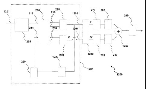
Figure 2 shows a schematic diagram of an optical receiving system 200 in
accordance with a
first embodiment of the present invention. The optical receiving system 200 is
comprised within the
end apparatus 120 of Fig. 1.
The optical receiving system 200 comprises a coherent optical receiving device
205 based
on a homodyne coherent receiving architecture with Costas optical phase locked
loop (OPLL). The
device 205 has an optical input port 201 optically connectable to the optical
link 130 and an electric
output port 203.
The coherent optical receiving device 205 comprises an optical hybrid 210
having a first input
port 212 optically connected to the input port 201 and a second input port 214
optically connected to a
local oscillator 260. The optical hybrid 210 further has a first pair of
output ports 216 optically
connected to a first differential photodetector 220 for outputting in-phase
components (0 and 180 ) of
the optical signal with respect to the local oscillator and a second pair of
output ports 218 optically
connected to a second differential photodetector 230 for outputting quadrature
components (90 and
270 ) of the optical signal with respect to the local oscillator. The optical
hybrid 210 of figure 2 is
exemplarily an eight-port 90 optical hybrid as shown in Figure 10(c) of the
Davis et al. article.
In an alternative configuration (not shown), the first and second
photodetector 220 and 230
are single-input photodetector each one coupled to one output port of,
respectively, the first and
second pair of output ports 216 and 218.
The coherent optical receiving device 205 further comprises a multiplier 240
electrically
connected, by way of electrical connecting lines, to the output of the first
and second differential
photodetector and an electrical loop filter 250 electrically interposed
between the output of the
multiplier 240 and an input of the local oscillator 260.
Alternatively to the Costas OPLL shown and described herein, it is possible to
use alternative
OPLL schemes suitable to PSK modulation, such as a balanced pilot-carrier PLL
or a decision-driven
loop, known in the art.
According to a preferred embodiment of the present invention, an electrical
filter 270 is
electrically connected to the output port 203 which in turn is electrically
connected to the output port of
CA 02703726 2010-04-23
WO 2009/071964 PCT/1B2007/054948
14
the first differential photodetector 220. In this embodiment the electrical
filter 270 is a low-pass filter.
Preferably, the filter 270 has ¨3dB double-side bandwidth greater than or
equal to 0.44R and lower
than or equal to 0.68R. More preferably, the ¨3dB double-side bandwidth is
greater than or equal to
0.50R and lower than or equal to 0.62R. Still more preferably, the ¨3dB double-
side bandwidth is
greater than or equal to 0.54R and lower than or equal to 0.58R.
Advantageously, the electrical filter
is a 5th-order Bessel filter having ¨3dB double-side bandwidth equal to about
0.56R, being R the bit-
rate of the DPSK optical signal.
A squarer or 'square-law' device 280 and a discriminating system 290 are
electrically
cascaded in the cited order downstream to the optical filter 270 with respect
to the direction of
propagation of the electrical signals. The discriminating system 290 comprises
a clock and data
recovery (CDR) circuit, a sampling circuit and a threshold discriminator.
A polarization stabilizer 295 is optically interposed between the input port
201 of the coherent
receiving device 205 and the first input port 212 of the optical hybrid 210.
The polarization stabilizer
295 may be for example of the type described in patent application
W003/014811.
In operation, the DPSK optical signal is received at the input port 201 of the
coherent optical
receiving device 205 after having propagated along the optical link 130 and is
mixed with the optical
field coming from the local oscillator 260 by way of the optical hybrid 210.
Before mixing, the
propagated DPSK optical signal is fed to the polarization stabilizer 295 which
stabilizes its time-
varying input polarization state into an output fixed polarization state, so
that at the input ports 212,
214 of the hybrid 210 the polarization state of the DPSK optical signal and
the optical field of the local
oscillator are in a fixed relationship (e.g. coincident). In this way the
amplitude of the mixed optical
signals at the output ports of the optical hybrid is made independent from the
polarization state of the
DPSK optical signal received at the input port 201.
The in-phase outputs (0 and 180 ) at the first pair of output ports 216 are
received by the
first differential photodetector 220, which outputs a first electrical signal
r directly proportional to an
in-phase component of the optical field of the DPSK optical signal with
respect to the optical field of
the local oscillator.
The quadrature outputs (90 and 270 ) at the second pair of output ports 218
are received by
the second differential photodetector 230, which outputs a second electrical
signal Q directly
proportional to a quadrature component of the optical field of the DPSK
optical signal with respect to
the optical field of the local oscillator.
In order to lock the phase (and hence the frequency) of the local oscillator
with that of the
received DPSK optical signal a Costas OPLL is exemplary used. Here, the first
and second electrical
CA 02703726 2010-04-23
WO 2009/071964
PCT/1B2007/054948
signal I and Q are multiplied in the block 240 and then filtered in the filter
250 of the feedback loop so
as to generate a signal for controlling the output optical frequency of the
local oscillator 260 (e.g., in
case the local oscillator is a laser diode, by controlling the driving
current). In this way the phase
stochastic fluctuations and the frequency drifts are compensated for. As a
result, the first electrical
5 signal / is kept to carry the information related to the propagated DPSK
signal while the second
electrical signal Q is kept about zero.
The first electrical signal / is filtered by the low-pass narrowband
electrical filter 270 so as
to obtain an (analog) three-level electrical signal (-1, 0, +1). Thereafter,
the filtered signal is squared
by the electrical squarer 280, so as to obtain an analog two-level electrical
signal (0, +1) which
0 represents the de-coding of the DPSK optical signal and which has an
improved extinction ratio and
high dispersion robustness. After being squared, the squared signal is passed
to the discriminating
system wherein it is sampled with a sampling rate equal to the bit-rate R and
with a clock recovered
from the squared signal itself. The values of the samples are thereafter
compared with a threshold in
order to obtain a digital binary electrical signal (output data signal) which,
apart from possible errors,
15 corresponds to the binary data signal fed to the pre-coder at the
transmitter side. The Applicant has
found that the above three-level electrical signal is intrinsically robust to
dispersion and such
robustness is maintained in the two-level output data signal.
Figure 3 shows a schematic diagram of an optical receiving system 300 in
accordance with a
first variant of the first embodiment of figure 2. Throughout the present
description and drawings, the
same reference numeral is used for the same element. Reference is done to the
description above for
all the features already introduced above.
The optical receiving system 300 mainly differs from the receiving system 200
of figure 2 in
that the polarization matching function of the polarization stabilizer 295 is
here performed by a
polarization transformer 395, of the type known in literature, acting on the
optical radiation emitted by
the local oscillator 260 so as to transform the fixed polarization of the
optical radiation into a varying
polarization having a stable relationship (typically coincident) to the one of
the DPSK signal, so that
the amplitude of the mixed signal is independent from the polarization of the
DPSK optical signal.
Therefore, the polarization transformer is optically interposed between the
local oscillator and the
optical hybrid 210. A controller 390 is electrically connected, by way of an
electrically connecting line,
to the output of the first photodetector 220 so as to receive in input the
first electrical signal I and is
operatively connected, e.g. by way of an electrical connecting line, to the
transformer 395 so as to be
able to drive the latter.
In use, the controller 390 receive in input the first electrical signal I
which, being an AC
CA 02703726 2010-04-23
WO 2009/071964 PCT/1B2007/054948
16
signal, has zero mean and is amplitude modulated between two opposite values
with rate equal to R.
The controller processes the first signal / calculating its envelope and then
low-pass filtering it with a
filter bandwidth 6, such that V 501 << B, << R, wherein Tp01 is the
characteristic time of the
fluctuations of the polarization. For DPSK optical signals having bit rate R
greater than or equal to 2.5
Gbit/s, a typical value of Bc lays in the interval between about 1 MHz and 50
MHz. The controller 390
then drives the polarization transformer 395 with a control signal, so as to
maximize the above filtered
envelope, for example using a known method of transforming a fixed
polarization state into a varying
polarization state matched to the one of the DPSK optical signal, such as for
example in article
"Polarization control for coherent fiber-optic systems using nematic liquid
crystals" by S. H. Rumbaugh
et al., Journal of Lightwave Technology, vol. 8, pages 459-465 (March 1990) .
Figure 4 shows a schematic diagram of an optical receiving system 400 in
accordance with an
alternative realization of the first variant of the first embodiment shown in
figure 3. The main difference
with respect to the example shown in figure 3 is that now the controller 490
is electrically connected to
the output of the squarer 280. In use, the controller 490 receives in input
the above squared electrical
signal, low-pass filters it according to the preceding paragraph and then
sends a feedback control
signal to the polarization transformer 395 so as to maximize the low-pass
filtered signal. The
advantage of this configuration is that the above step of calculating the
envelope is avoided, thanks to
the fact of processing the squared electrical signal.
Figure 5 shows a schematic diagram of an optical receiving system 500 in
accordance with a
preferred realization of the first embodiment of figure 2. The main difference
with the latter is that now
an electrical (chromatic) dispersion compensator (EDC) 510 is placed
downstream the
photodetector(s) with respect to the direction of propagation of the
electrical signals. Due to the
linearity of both the EDC 510 and the filter 270, the EDC may be placed
upstream (as shown in figure
5) or downstream (not shown) the filter 270, but in any case it is placed
upstream the squarer 280. In
the latter case (not shown) a pair of filters 270 are electrically interposed
between the first
photodetector 220 and the EDC 510 and, respectively, between the second
photodetector 230 and
the EDC 510 (in a configuration similar to the one shown in figure 7 below).
As regard the polarization matching system, it is possible to adopt either the
solution shown in
figure 5, contemplating the polarization stabilizer 295, or alternatively
either one of the solutions
shown in figures 3 or 4, contemplating the polarization transformer 395.
The EDC 510 is a linear analog base-band EDC based on electrical tapped delay-
line
equalizers or multi-tap transversal filters. A tapped delay-line equalizer (or
N-tap transversal filter)
CA 02703726 2010-04-23
WO 2009/071964
PCT/1B2007/054948
17
contains N delay lines, each having a delay equal to an integer multiple of a
given time period T, such
integer multiple increasing by one unit when passing from one delay line to
the successive one. Each
delay line has a variable gain amplifier (VGA). The gains and the delays
should remain substantially
constant within the spectral bandwidth of the above narrow-band electrical
filter 270 . The analog
tapped delay-line equalizer performs a linear combination of N replica of a
signal component (in-
phase or quadrature), the replica being retarded by a progressively increasing
integer multiple of the
given time period T.
Figure 6 shows in terms of functional blocks a schematic diagram of an
exemplary base-band
analog linear EDC 510. It comprises four tapped delay-line equalizers (or four
N-tap transversal filters)
610, 620, 630 and 640 each synthesizing a respective transfer function, and a
pair of adders 650. All
four tapped delay-line equalizers are based on the same given time period T.
In use, the EDC 510 receives at its input ports respectively the above first
(in-phase) and
second (quadrature component) signals I and Q and transform them into output
compensated signal l'
and Q', even thought the latter is not used in the present embodiment, by
implementing a transfer
function which approximates the inverse of the transfer function, translated
in base-band, given by
the chromatic dispersion of the optical link 130. In this way an efficient
compensation of the dispersion
is obtained. The compensated in-phase quadrature signal l' is then filtered
(filter 270), squared
(squarer 280) and discriminated (290) as described above.
In case the EDC 510 is placed downstream the pair of filters 270, as described
above, both
the first and second components signals I and Q are first filtered in
accordance with the present
invention and then fed into the EDC in order to be processed as above.
The Applicant has found that it is advantageous to choose the above given time
period T
equal to Tn.:1/R, being Tbit the period of a bit of the DPSK optical signal.
More in details, the
Applicant has found that the choice of T= Tbit for the above combination of a
DPSK modulation format,
a coherent receiver, a narrow-band electrical filter and a squarer, has proven
to provide a greater
robustness to the dispersion with respect to a comparative choice of T= Tn/2,
for the same number N
of taps. With the above choice and N=9, it is possible to obtain a 'reach'
(exemplary defined in
correspondence of a 2 dB penalty due to the dispersion) of about 670 km of
conventional SMF at 10
Gbit/s. The Applicant has also found that by slightly increasing over Tbit the
value of T it is possible to
further extend the reach (e.g. 790 km of conventional SMF, with N=9 and
T=1.15/R, as shown in
figure 22).
Figure 7 shows a schematic diagram of an optical receiving system 700 in
accordance with a
further realization of the embodiment of figure 5, with the difference that
now the dispersion
CA 02703726 2010-04-23
WO 2009/071964
PCT/1B2007/054948
18
compensation is performed digitally instead of analogically.
A pair of filters 270, each one in all identical to the narrow-band filter 270
described above,
are electrically connected to the output of respectively the first and second
photodetectors 220, 230. A
digital processor 710, e.g. of digital signal processor (DSP) type, has its
two input ports connected to
the output of the filters 270, respectively. The processor 710 comprises a
digital EDC 720, a digital
squarer 730 and a discriminator 740.
Figure 8 shows in terms of functional blocks the scheme of the digital EDC
720. It comprises
a pair of analog to digital converters 810 (ADC) respectively connected to the
input ports of the EDC
and respectively followed by a pair of digital tapped delay-lines or digital N-
tap transversal filters 800.
Each of the latter comprises a shift-register 820 (having N memory cells) and
an equalizer 830.
Referring back to figure 7, a clock recovery circuit 750 is connected to the
output of the first
photodetector and is configured to distribute a clock recovered from the in-
phase component of the
received DPSK signal to the EDC 720, the squarer 730 and the discriminator
740.
In use, the above first (in-phase component) and second (quadrature component)
signals I
and Q are filtered by a respective low-pass narrowband filter 270 in
accordance to the present
invention. Preferably, each of the filter 270 has ¨3dB double-side bandwidth
greater than or equal to
0.44R and lower than or equal to 0.68R. More preferably, the ¨3dB double-side
bandwidth is greater
than or equal to 0.50R and lower than or equal to 0.62R. Still more
preferably, the ¨3dB double-side
bandwidth is greater than or equal to 0.54R and lower than or equal to 0.58R.
Advantageously, the
electrical filter is a 5th-order Bessel filter having ¨3dB double-side
bandwidth equal to about 0.56R.
The filtered components are then fed to the digital EDC 720 and sampled by the
respective ADC 810
with a sampling rate S. The electrical pass-band of the ADCs should be large
enough to comprise the
spectral region wherein the filtered components are significantly different
from zero, in order to avoid
signal distortion. The sampled signals are then processed by the digital N-tap
transversal filters 800
as shown in figure 8. Each of the N-tap transversal filters 800 runs an
algorithm which processes
contiguous sets of N samples, being N equal to the number of taps of the
filter. The shift-register 820
stores in its N cells the N samples. The equalizer 830 then calculates, at a
rate S, a linear combination
of the N stored samples with coefficients chosen in accordance to the transfer
function of the optical
link 130. The clock recovery circuit 750 distributes the clock S recovered
from the received DPSK
signal to the EDC 720 (and the squarer 730 and the discriminator 740).
The Applicant has found that it is advantageous to choose the above rate S
equal to the
DPSK bit-rate R (synchronous equalizer). One advantage of this solution with
respect to a digital
fractionally spaced equalizer (wherein the rate S is a multiple of the bit-
rate R) is that the required
CA 02703726 2010-04-23
WO 2009/071964
PCT/1B2007/054948
19
sampling and processing rate is lower, while extending the reach.
Figure 9 shows a schematic diagram of an optical receiving system 900 in
accordance with a
second embodiment of the present invention. .
The optical receiving system 900 comprises a heterodyne coherent optical
receiving device
905 based on a heterodyne coherent receiving architecture. The receiving
device 905 having an
optical input port 901 optically connectable to the optical link 130 and an
electric output port 903.
The coherent optical receiving device905 comprises an optical hybrid 910
having a first input
port 912 optically connected to the input port 901 and a second input port 914
optically connected to a
local oscillator 260. The optical hybrid 910 further has a first output port
916 optically connected to a
0 first input of a differential photodetector 920 and a second output port
918 optically connected to a
second input of the differential photodetector 920, for outputting both in-
phase (0 and 180 )
components of the optical signal with respect to the local oscillator. The
optical hybrid 910 of figure 9
is exemplarily a four-port 180 optical hybrid as shown in Figure 10(a) of the
Davis et al. article.
In an alternative configuration (not shown), the photodetector 920 is a single-
input
photodetector coupled to only one of the first and second output ports 916 and
918.
A wide-band electrical filter 940 is electrically connected to the output port
903 which in turn is
electrically connected to the output port of the differential photodetector
920. The wide-band electrical
filter 940 is a pass-band electrical filter centered at the intermediate
frequency and having a -3dB
double-side bandwidth greater than R, in order to suppress the out-of-band
noise. It is preferable that
2 0 the wide-band filter 940 has a response sufficiently flat around the IF
in order not to distort the signal.
A polarization stabilizer 295 as described above is optically interposed
between the input port
901 of the coherent receiver 905 and the first input port 912 of the optical
hybrid 910. In an alternative
configuration, the polarization stabilizer is replaced by a polarization
transformer and a controller as
shown and described with reference to either figure 3 or figure 4.
Optionally, an optical frequency locking loop (0FLL) is envisaged, comprising
an intermediate
frequency (IF) locking circuit 950 electrically connected to the output of the
filter 940 (or directly the
output of the photodetector). In case the laser source at the transmitter side
is sufficiently stable (e.g.
having a drift less than about 0.2 R), the OFLL may advantageously be avoided.
The optical receiving system 900 further comprises an electrical circuit 960
for synchronous
heterodyne demodulation. It comprises an electrical phase locked loop (EPLL)
comprising, in addition
to the wide-band electrical filter 940 above, a pair of multipliers 962, a 90
phase shifter 964, an
oscillator 966, a loop filter 968 and a further multiplier 969. In accordance
to an embodiment of the
present invention, the receiving system further comprises a pair of narrow-
band electrical filters 270.
CA 02703726 2010-04-23
WO 2009/071964
PCT/1B2007/054948
Each of the electrical filters 270 is a 5th-order Bessel low-pass filter
having ¨3dB double-side
bandwidth equal to about 0.56R, being R the bit-rate of the DPSK optical
signal.
A squarer or 'square-law' device 280 and a discriminating system 290, of the
kind described
above, are electrically cascaded in the cited order downstream to the optical
filter 270 with respect to
5 the direction of propagation of the electrical signals.
In operation, the DPSK optical signal is received at the input port 901 of the
coherent optical
receiver 905 after having propagated along the optical link 130 and is mixed
with the optical field
coming from the local oscillator 260 by way of the optical hybrid 910. Before
mixing, the input
polarization state of the propagated DPSK optical signal is matched to that of
the optical field of the
10 local oscillator as described above.
The in-phase outputs (0 and 180 ) at the output ports 916, 918 are received
by the
differential photodetector 920, which outputs an electrical signal which
modulates an electrical carrier
at a frequency equal to the difference between the optical frequency of the
DPSK signal and the
optical frequency of the local oscillator. The OFLL (950) controls the output
optical frequency of the
5 local oscillator 260 in such a way that the above difference is kept
substantially constant close to a
predetermined value called intermediate frequency (IF) value. The IF is
selected between R and 3R,
preferably between 1,5R and 2,5R.
The above electrical signal, which carries the information related to the
propagated DPSK
signal, is then fed to the electrical circuit 960 in order to be synchronously
demodulated as known in
20 the art. At the output of the circuit 960 an (analog) three-level base-
band electrical signal (-1, 0, +1) is
obtained. Thereafter, the filtered signal is squared by the electrical squarer
280, so as to obtain an
analog two-level electrical signal (0, +1) which represents the de-coding of
the DPSK optical signal
and which has an improved extinction ratio and enhanced dispersion robustness.
After being squared,
the squared signal is passed to the discriminating system wherein it is
processed as explained above.
Figure 10 shows a schematic diagram of an optical receiving system 1000 in
accordance with a
variant of the second embodiment of the present invention. The optical
receiving system 1000 of
figure 10 is based on synchronous demodulation comprising an IF carrier
recovery circuit 1010. The
latter is connected to the output of the wide-band filter 940. It comprises an
electrical radio-frequency
voltage controlled oscillator (RF-VCO) phase-locked through an EPLL suitable
for PSK format
(characterized by carrier suppression), such as for example a squaring loop
1010.
As regard the polarization matching system, either a polarization stabilizer
295, as shown in
figure 10, or a polarization transformer 395, as shown in figures 3 or 4 may
be used as described
above.
CA 02703726 2010-04-23
WO 2009/071964
PCT/1B2007/054948
21
In use, the above electrical signal is first filtered by way of the pass-band
wide-band filter 940
(identical to the filter 940 of fig 9) centered on the intermediate frequency
and then it is multiplied, by
way of the multiplier 1020, by the carrier recovered from the electrical
signal itself by the IF carrier
recovery circuit 1010. The baseband electrical signal thus obtained is then
filtered by a narrow-band
low-pass filter 270 in accordance to the present invention, squared and
discriminated as explained
above. In case of a squaring loop 1010, the input electrical signal is first
squared, pass-band filtered,
multiplied by an electrical oscillator output signal and low-pass filtered by
way of a loop filter in order
to obtain a control of the emission frequency of the electrical oscillator.
Finally, the carrier thus
generated by the electrical oscillator is divided by 2 so as to obtain the
recovered carrier.
Figure 11 shows a schematic diagram of an optical receiving system 1100 in
accordance with
the variant of the second embodiment of the present invention shown in figure
10, further provided
with an EDC 1120 in order to improve the robustness to dispersion. The EDC
1120 is usable also in
the receiving system 900 of figure 9. The EDC is an analog EDC having a pass-
band centered around
the IF. It is possible to provide a pass-band EDC 1120 based on tapped-delay
line equalizers or N-tap
5
transversal filters. In one realization, the EDC 1120 is realized by a tapped-
delay line equalizer or an
N-tap transversal filter, wherein for each tap both the gain and the phase
shift are adjusted. In a
further realization, the EDC 1120 is based on the scheme as shown in fig.2 of
the cited Winters article,
comprising a quadrature electrical hybrid and a pair of tapped-delay line
equalizers or N-tap
transversal filters having only the gains controllable.
In a still further realization, the pass-band EDC 1120 is realized by a
dispersive microwave
waveguide or a dispersive microstrip line, both having a suitable chromatic
dispersion around the IF.
The Applicant has found that the combination of the DPSK modulation format,
the coherent
receiving device, the narrow-band electrical filtering and the squaring allows
choosing the above time
period T (equal to the delay between two successive taps) equal to Tbit=1/R
(synchronous tapped
delay-line equalizer). Moreover, the Applicant has found that the choice of T
comprised between
0.7/R and 1.4/R (including T= Tbit) for the above combination of a DPSK
modulation format, a
coherent receiving device, a narrow-band electrical filter and a squarer, has
proven to provide a
greater robustness to the dispersion with respect to an exemplary comparative
choice of T= Tht/2, for
the same number N of taps (see also figure 22 below).
As regard the polarization matching system, either a polarization stabilizer
295 of the type
shown in figure 2, or a polarization transformer 395 of the type shown in
figure 3 or in figure 4, may be
used as described above.
With reference to figure 11, a polarization transformer 395 is driven by a
controller 1190
CA 02703726 2010-04-23
WO 2009/071964 PCT/1B2007/054948
22
receiving in input the above electrical signal (of AC type centered at a
frequency near IF). The
operation of the controller 1190 and of the polarization transformer 395 is
similar to that described for
the controller 390 and the transformer 395 of figure 3.
Alternatively, when the scheme of figure 4 is adopted for the polarization
matching system,
the controller 1190 accepts in input the base-band signal after being squared.
The operation of the
controller 1190 and of the polarization transformer 395 is similar to that
described for the controller
490 of figure 4.
Figure 12 shows a schematic diagram of an optical receiving system 1200 in
accordance with
a third embodiment of the present invention. The optical receiving system 1200
is comprised within
the end apparatus 120 of Fig. 1. The optical receiving system 1200 comprises a
phase diversity
coherent optical receiving device 1205 having an optical input port 1201
optically connectable to the
optical link 130 and a first and a second electric output port 1203, 1204.
The coherent optical receiving device 1205 comprises an optical hybrid 210, a
local oscillator
260, a first and a second differential photodetector 220, 230 as shown and
described with reference to
figure 2. In an alternative configuration (not shown), the first and second
photodetector 220 and 230
are single-input photodetector with AC output each one coupled to one output
port of, respectively, the
first and second pair of output ports 216 and 218, as described above.
In a still further alternative configuration, the optical hybrid 210 may be a
six-port hybrid in
combination to a third single-input photodetector.
Optionally, the coherent optical receiver 1205 further comprises an OFLL
electrical circuit
1220 electrically connected to the output of the first photodetector 220 and
to the input of the local
oscillator 260. The OFLL circuit 1220 is configured to keep low (e.g. below
0.02R) the frequency
difference, in absolute value, between signal and local oscillator.
Two electrical filters 270 are electrically connected respectively to the
output port 1203, which
in turn is electrically connected to the output port of the first differential
photodetector 220, and to the
output port 1204, which in turn is electrically connected to the output port
of the second'differential
photodetector 230. According to the present embodiment, each of the two
electrical filters 270 is a
low-pass filter having -3dB double-side bandwidth comprised between 0.44R and
0.68 R. Preferably,
each electrical filter 270 is a 5th-order Bessel low-pass filter having ¨3dB
double-side bandwidth equal
to about 0.56R, being R the bit-rate of the DPSK optical signal.
Two squarers 280 are electrically connected respectively to the output port of
the two
electrical filters 270, and their output ports are both connected to an adder
1250. A discriminating
system 290, of the kind described above, is connected to the output port of
the adder 1250.
CA 02703726 2010-04-23
WO 2009/071964
PCT/1B2007/054948
23
As regard the polarization matching system, a polarization stabilizer 295 is
optically
interposed between the input port 1201 of the coherent receiver 1205 and the
first input port 212 of
the optical hybrid 210. The polarization stabilizer 295 may be for example of
the type described in
patent application W003/014811.
In operation, the received DPSK optical signal is polarization stabilized,
mixed with the local
oscillator 260 and photodetected as described with reference to the first
embodiment of the present
invention. The first photodetector 220 emits a first electrical signal I,
which is directly proportional to
an in-phase component of the DPSK optical signal with respect to the phase of
the local oscillator,
and the second photodetector 220 emits a second electrical signal Q, directly
proportional to a
quadrature component of the DPSK optical signal.
Since the local oscillator is not locked in phase to the DPSK signal (but
possibly only in
frequency), the stochastic fluctuations of the phase difference generates a
stochastic rotation of the
two-point (0 - 1800) field constellation in the complex plane having axes /
and Q.
Both the first electrical signal / and the second electrical signal Q are
filtered by the
respective low-pass narrowband electrical filter 270 in order to obtain a
three-point field constellation
stochastically rotating. Both the first and the second filtered electrical
signal are thereafter squared by
the respective squarer 280 and the squares are summed by the adder 1250, in
order to eliminate the
dependency from the above phase difference and to obtain a two-level
electrical signal. The latter
signal, i.e. the sum of the squared electrical signals at the output of the
adder 1250, is thereafter fed to
the discriminating system 290 as described above.
Optionally and preferably, the optical receiving system 1200 comprises an
analog EDC 1230
having a pair of input port respectively connected to the output of the first
and second photodetector
220, 230 and a pair of output port respectively connected to the input of the
pair of filters 270. The
analog EDC 1230 is, e.g., of the kind described with reference to figure 6.
Preferably it is a
synchronous EDC.
Due to the linearity of the EDC and the filters 270, it is possible to place
the pair of filters 270
upstream the EDC with respect to the direction of propagation of the
electrical signals (from left to
right in figure).
Figure 13 shows a schematic diagram of an optical receiving system 1200 in
accordance with
the third embodiment of the present invention shown in figure 12, wherein now
the dispersion
compensation is performed digitally instead of analogically.
A digital processor 1330, e.g. of DSP type, has its two input ports connected
to the output of
the filters 270, respectively. The processor 1330 comprises a digital EDC 720,
of the kind described
CA 02703726 2010-04-23
WO 2009/071964 PCT/1B2007/054948
24
with reference to figures 7 and 8, a pair of digital squarers 730, a digital
adder 1340 and a digital
discriminator 740.
A clock recovery circuit 750 is connected to the output of the first
photodetector and is
configured to distribute to the digital processor 1330 a clock recovered from
the electrical signals
and Q (after or before filtering). Similarly to the above, the Applicant has
found that it is advantageous
to choose the above rate S equal to the DPSK bit-rate R (synchronous
equalizer).
Figure 14 shows a schematic diagram of an optical receiving system 1400 in
accordance with
a variant of the third embodiment of the present invention shown in figure 12.
In this variant, the OFLL 1420 is now configured for keeping the frequency
difference in
0 absolute value between the DPSK signal and the local oscillator equal to
an intermediate frequency
(IF) greater than R, preferably comprised between 1.5R and 2.5R. In this case,
the narrow-band
electrical filters 270 of the embodiment shown in figure 12 are replaced by a
pair of pass-band
electrical filters 1470 each centered at the IF and having -3dB double-side
bandwidth comprised
between 0.44R and 0.68 R. Preferably each of the pass-band electrical filter
is a 5th order pass-band
Bessel filter having -3dB double-side bandwidth equal to 0.56.
Optionally and preferably, the optical receiving system 1400 comprises an
analog EDC 1430
comprising a pair of separate analog pass-band EDCs 1120 of the kind described
with reference to
figure 11. Each of the pass-band EDC 1120 has an input port connected to the
output of the
respective photodetector 220, 230 and an output port connected to the input of
the respective filter
1470. Due to the linearity of the EDC and the filters, it is possible to place
the pair of filters 1470
upstream the EDC.
In use, both the electrical signals I and Q coming from the photodetectors are
frequency
translated at a central frequency near the IF. Each of the pass-band EDC 1120
acts separately on the
respective signal I and Q, emitting the compensated signal l' and Q'.
As regard the polarization matching system for the third embodiment (in all
its variants) of the
invention, several schemes may be adopted in addition to the one shown in
figures 12-14.
Figure 15 shows one of the possible polarization matching schemes suitable to
all the variants
shown in figures 12, 13 and 14. In this respect, the narrow-band filters 1570
may be either the low-
pass filter 270 of figure 12 and 13 or the pass-band filters 1470 of figure 14
and the optional EDC
1530 may be either the low-pass EDC 1230 of figure 12 or the pass-band EDC of
figure 14.
Alternatively to the EDC, the DSP 1330 of figure 13 may be optionally
employed.
In figure 15 the polarization matching function is performed by a polarization
transformer 395,
of the type described above (see e.g. figures 3 and 4), acting on the optical
radiation emitted by the
CA 02703726 2010-04-23
WO 2009/071964
PCT/1B2007/054948
local oscillator 260 so as to transform the fixed polarization of the optical
radiation into a varying
polarization having a stable relationship (typically coincident) to the one of
the DPSK signal. A
controller 1590 has its input ports electrically connected respectively to the
output of the first and
second photodetector 220,230 so as to receive in input at least one of the
first and second electrical
5
signal / and Q and has its output port operatively connected, e.g. by way of
an electrical
connecting line, to the transformer 395 so as to be able to drive the latter.
In use, in the variant of the third embodiment wherein the frequency
difference in absolute
value between local oscillator and DPSK signal is kept by the OFLL 1220 near
the IF, as explained
with reference to figure 14, the controller 1590 receives in input at least
one (preferably only one) of
0 the
AC electrical signals / and Q (phase modulated 0 - 180 at rate R and
frequency translated
around IF). The controller calculates its envelope and then low-pass filters
it with a filter bandwidth Bc
such that 1/ r P 1 B, R , wherein 2-pot is the characteristic time of the
fluctuations of the
polarization. For DPSK optical signals having bit rate R greater than or equal
to 2.5 Gbit/s, a typical
value of Bc lays in the interval between about 1 MHz and 50 MHz.
15 In
the variant of the third embodiment wherein the frequency difference in
absolute value,
called 'Offset
between local oscillator and DPSK signal is kept by the OFLL 1220 less than
0.02R,
see figures 12 and 13, then it is preferable that such frequency difference is
kept by the OFLL different
from zero, such that 1/501 << B, foffiet R. Being r pot typically greater
than 1 ms,
when R is greater than or equal to 2.5 Gbit/s it is advantageous to select
foffiet in the interval
20
between 20MHz and 50 MHz and Bc not greater than about 1 MHz. In this case,
advantageously the
controller 1590 may receive in input only one of the AC electrical signals /
and Q.
In both the above variants, the controller 1590 drives the polarization
transformer 395 with a
control signal, so as to maximize the above filtered envelope as explained
above.
Figure 16 shows another of the possible polarization matching schemes suitable
to all the
25
variants shown in figure 12, 13 and 14. The main difference with respect to
the example shown in
figure 14 and described above is that now the input port of the controller
1690 is electrically connected
to the output of the adder 1250. In use, the controller 1690 receives in input
the above sum of squared
electrical signals, low-pass filters it and then sends a feedback control
signal to the polarization
transformer 395 so as to maximize the low-pass filtered signal. Figure 17
shows a further possible
polarization matching scheme (based on polarization diversity) suitable to all
the variants shown in
figure 12, 13 and 14, without the polarization stabilizer 295.
CA 02703726 2010-04-23
WO 2009/071964
PCT/1B2007/054948
26
Here, the polarization matching system comprises an optical polarization
splitter 1710 having
its optical input port 1701 optically connected to the link 130. For example,
the splitter 1710 may be a
polarizing beam splitter (PBS) in free-space or a planar lightguide circuit
(PLC) polarization splitter in
integrated optics. The splitter 1710 has a pair of output ports for outputting
respectively two
components of the propagated DPSK optical signal having polarizations x and y,
for example
orthogonal. Each of the two output ports x and y of the splitter 1710 is
connected to the first input port
212 of a respective optical hybrid 210. Each of the optical hybrid 210 is then
connected to a cascade
of elements (photodetectors 220, 230, optional EDC 1530, narrow-band filters
1570, which have
according to the present invention -3dB double-side bandwidth comprised
between 0.44R and 0.68 R,
squarers 280 and adder 1250) as described with reference to figures 12, 13 and
14. A further adder
1750 has its input ports connected to the output of the two adder 1250 and its
output port to the
discriminating system 290.
A single local oscillator 260 is optically connected to the input port of a
further optical
polarization splitter 1730, similar to the splitter 1710, which in turn has
its pair of output ports
respectively connected to the respective second input port 214 of one of the
two optical hybrids 210,
for outputting respectively two components of the oscillator field having the
same above polarizations
x and y. The polarization of the field of the local oscillator is oriented so
that it is split in the two
polarized components x and y having equal power.
Optionally, a OFLL 1720 has its two input ports connected to the output port
of the two first
photodetectors 220, respectively, and its output port connected to the local
oscillator 260 so as to
control its emission frequency.
In use, the propagated DPSK optical signal is received at the input port 1701
of the
polarization splitter and is split in its two orthogonally polarized
components x and y, which are then
coherently received in accordance to the description above (see figures 12 and
14). The two electrical
signal thus obtained are summed up at the element 1750 and the result is then
discriminated. The
field of the local oscillator is split in its two (orthogonally) polarized
components x and y, so that each
of the hybrid 210 mixes the same polarization component of the signal and
local oscillator. In case
the hybrid is in integrated optics (such as a PLC hybrid), then it is
preferable that the splitter 1710 is a
polarization splitter and rotator so that the two polarizations x and y are
coincident. In this case the
splitter 1730 may simply be a 3dB beam splitter.
Figure 18 shows a schematic diagram of an optical receiving system 1800 in
accordance with
a fourth embodiment of the present invention. The optical receiving system
1800 is comprised within
the end apparatus 120 of Fig. 1. . The optical receiving system 1800 comprises
a heterodyne
CA 02703726 2010-04-23
WO 2009/071964 PCT/1B2007/054948
27
coherent optical receiving device 1805 based on a double-stage phase diversity
coherent receiving
architecture. The receiving device 1805 comprises a phase diversity coherent
optical receiving device
1205 in all similar to the one described with reference to figures 12 and 13.
The heterodyne coherent
optical receiving device 1805 also comprises an IF electrical local oscillator
1810 (second-stage) for
sending an IF signal and its replica, phase shifted by 90 by way of a 90
phase shifter 1820,
respectively in input to a pair of multipliers 1830. The latter are also
connected respectively to the
output port of the pair of photodetectors. An adder 1850 is connected to
receive in input the output of
the multipliers 1830 and to output their sum at the output port 903. Connected
to the latter, a
synchronous heterodyne demodulator 960, a squarer 280 and a discriminating
system 290 are
0 connected in cascade. The elements 280 and 290 are of the kind previously
described, in accordance
to the present invention. The electrical circuit 960 for synchronous
heterodyne demodulation is
configured for shifting back the signal at base-band. It may exemplarily be
the same as of the EPLL
960 shown in figure 9, which comprises a pair of low-pass filters 270 in
accordance to the present
invention. Alternatively to the EPLL 960, an IF carrier recovery circuit 1010
may be employed,
together with the multiplier 1020, the pass-band filter 940 and the low-pass
filter 270 as shown in
figure 10.
Optionally, a pass-band analog EDC 1120 of the kind described with reference
to figure 11
may be employed as shown in figure 18.
As regard the polarization matching system, either a polarization stabilizer
295 (not shown) or
a polarization transformer 395 (not shown) may be employed as previously
described.
In use, the received DPSK optical signal is polarization matched, mixed with
the local
oscillator 260 and photodetected as described with reference to the first and
third embodiments of the
present invention, in order to obtain the above first electrical signal i and
second electrical signal Q.
The second stage (elements 1810, 1820 and 1830) then shifts both the signals
at the intermediate
frequency IF, comprised between 1.5R and 2.5R, thus obtaining an electrical
signal at a central
frequency near the IF in all similar to the one obtained by the heterodyne
coherent receiver 905 of
figures 9-11 without the pass-band wide-band filter 940. Thereafter, the
signal, possibly dispersion
compensated by the pass-band EDC 1120, in case it is present, is shifted back
to base-band by the
heterodyne demodulator 960, comprising the narrow-band filtering in accordance
to the present
invention. The subsequent processing (squaring and discriminating) is
thereafter the same as
previously described.
Unless the optical sources of the transmitter side and the local oscillator
are per-se sufficiently
stable in frequency, the OFLL 1220 operates to keep low the frequency offset
(below 0.02R).
CA 02703726 2010-04-23
WO 2009/071964
PCT/1B2007/054948
28
Figure 19 shows a schematic diagram of an optical receiving system 1900 in
accordance with
a variant of the above fourth embodiment of the present invention, wherein now
the optional
dispersion compensation is performed by a base-band analog EDC 1230, placed
between the phase
diversity receiver 1205 and the multipliers 1830. The base-band EDC 1230 is
configured and operates
as described with reference to figures 5, 6 and 12.
Figures 20, 21 and 22 show the optical signal to noise ratio (OSNR) versus the
dispersion
accumulated along the optical link 130 in various configurations of the
optical communication system
100. The graphs shown are results of numerical simulations run by the
Applicant, considering a NRZ-
DPSK modulation format with a bit-rate R equal to 10 Gbit/s, and the receiving
system 1200 as the
one shown in figure 12 (based on a phase-diversity scheme). The OSNR shown is
defined as the
OSNR, at a resolution equal to 0.5nm, needed in order to obtain a bit error
rate (BER) equal to 10-6, in
the hypothesis that the dominant noise comes from the amplified spontaneous
emission (ASE) of the
optical amplifiers 140 along the optical link.
Figure 20 shows the above OSNR corresponding to a double-side -3dB bandwidth
of the
5 narrow-band 5th order Besse' filters 270 respectively equal to 4.0 Ghz
(dashed curve 2010), 4.8 Ghz
(thin continuous curve 2020), 5.6 Ghz (thick continuous curve 2030), 6.8 Ghz
(dash-dotted curve
2040) and 9.0 Ghz (dotted curve 2050), without the EDC 1230. As can be seen,
the optimal value of
the filter bandwidth lays between about 4.4Ghz and 6.8 GHz.
Figure 21 shows the above OSNR corresponding to a double-side -3dB bandwidth
of the
narrow-band Bessel filters 270 respectively equal to 4.0 Ghz (dashed curve
2110), 4.6 Ghz (thin
continuous curve 2120), 5.6 Ghz (thick continuous curve 2130), 6.2 Ghz (dot-
dashed curve 2140) and
8.0 Ghz (dotted curve 2150), in presence of a synchronous (T=100ps) EDC 1230
with 9 taps.
Figure 22 shows the above OSNR corresponding to a double-side -3dB bandwidth
of the
narrow-band Bessel filters 270 equal to 5.6 Ghz, respectively without EDC
(thin continuous curve
2210), with a fractionally spaced (T=50 ps) 9-tap EDC (dotted curve 2220),
with a 9-tap EDC having
T=70ps=0.7/R (dashed curve 2230), with a synchronous (T=100ps) 9-tap EDC
(thick continuous curve
2240), with a 9-tap EDC having T=115 ps (thick dashed curve 2250) and with a 9-
tap EDC having
T=140ps=1.4/R (dot-dashed curve 2260). As can be seen, in absence of EDC the
scheme of the
present invention allows a reach (defined as 2 dB of additional penalty) of
about 3200 ps/nm, far
greater than traditional on-off keying (00K) direct detected system. Moreover,
a fractionally spaced
EDC leaves substantially unaltered the dispersion robustness, while the
choices of 1=100 ps and
T=115 ps allows a reach of respectively 10700 ps/nm (corresponding to about
670 km of conventional
fiber) and 12600 ps/nm (790 km of fiber).
CA 02703726 2010-04-23
WO 2009/071964 PCT/1B2007/054948
29
It is noted that the same numerical results shown in figures 20-22 are
obtained considering a
homodyne receiver 205 as shown in figure 2 with an ideal optical PLL.
Figure 23 shows a schematic diagram of a polarization division multiplexing
(PolDM) optical
communication system 2300 according to a further embodiment of the present
invention. Here, a pair
of the above transmitters 110 are followed by a polarization combiner 2310 apt
to multiplex the two
DPSK optical signals received respectively by the two transmitters 110, in an
orthogonal relationship
of their optical polarizations. At the opposite end of the optical link 130, a
polarization stabilizer 295 of
the kind described above is followed by a polarization splitter 2340. A pair
of the above end
apparatuses 120 is connected to the two output ports of the splitter 2340 in
order to receive a single
0 DPSK optical signal.
In use, the polarization combiner multiplexes together the two DPSK optical
signals with an
orthogonal relationship. Preferably, the two DPSK optical signals are RZ-DPSK
signals, and they are
time-interleaved in the resulting PolDM optical signal. After propagating
along the link 130, the
polarization stabilizer aligns the PolDM optical signal to the polarization
splitter 2340, so that the latter
5 separates the two single DPSK signals and send them respectively to a
respective end apparatus 120
in accordance to the present invention. It is noted that in this case each of
the end apparatus 120 has
in input a DPSK signal already stabilized in polarization, so that no further
polarization matching
system is required.
In case the end apparatuses 120 are based on synchronous heterodyne receivers
(figures 9-
20 11), on phase diversity receivers (figure 12-14) or on double-stage
phase diversity receivers (figures
18-19), advantageously a single source followed by a polarization splitter
acts as local oscillator for
both the end apparatuses 120. In this case, a single OFLL circuit keeps
constant the offset between
the frequency of one of the two DPSK signals (the latter being mutually
locked) and the frequency of
the local oscillator.
25 Although the present invention has been disclosed and described by way
of some
embodiments, it is apparent to those skilled in the art that several
modifications to the described
embodiments, as well as other embodiments of the present invention are
possible without departing
from the essential features thereof/the scope thereof as defined in the
appended claims.