Note: Descriptions are shown in the official language in which they were submitted.
CA 02703933 2010-04-23
WO 2009/058297
PCT/US2008/012266
LED LIGHT CONTROLLER SYSTEM AND METHOD
RELATED APPLICATIONS
[0001] This
application claims priority under 35 U.S.C. 119 to United States
Provisional Patent Application No. 61/000,804 filed on October 29, 2007, the
entire contents
of which is incorporated herein by reference.
BACKGROUND
[0002] Light
emitting diodes (LEDs) are used in various types of landscape, pool, and spa
lights and can be connected to a control system to output various color shows.
Conventional
methods for selecting color output are accomplished by turning alternating
current (AC)
power from a mains supply line on and off with an AC switch. However, with a
multitude of
fixed colors and color shows that can be selected, it becomes very tedious for
the user to
select a show by means of toggling an on/off switch.
[0003] Current
systems for controlling LED landscape, pool, and spa lights include a
microcontroller circuit that outputs pulse-width modulated (PWM) signals to
the LEDs. In
these systems, LEDs of various colors are necessary and the PWM signals
control the
intensity of the LEDs to produce various colors and effects.
SUMMARY
[0004]
Embodiments of the disclosure provide a system for selecting a color show
generated by LED landscape, pool, and/or spa lights or sources. The system can
include an
overlay indicating the color shows available to select from. The system
includes a selector
adjacent to the overlay, such as a rotary switch, positioned to select one of
the color shows.
The system includes a microcontroller in communication with the selector and a
triac circuit
in communication with the microcontroller. The microcontroller controls the
LED landscape,
pool, and/or spa lights using the triac circuit in response to the position of
the selector.
[0005] In some
embodiments, the triac provides communication between an AC source
and the LED sources. The triac receives signals from the microcontroller based
on the data
received from a user interface, such as the selector. The triac clips the
voltage from the AC
CA 02703933 2015-09-14
2
source to the LED sources in order to provide one or more voltage pulses to
the LED
sources based on the signals received from the microcontroller.
[0006] In some
embodiments, the system includes an output power trace from the AC
source to the LED sources. The system can also include a sensing circuit
positioned near
the output power trace to detect a characteristic of the output power trace.
The sensing
circuit can transmit data to the microcontroller corresponding to the
characteristic of the
output power trace. The microcontroller can control the LED sources based on
the data
transmitted by the sensing circuit.
[0006A] In one broad aspect of the invention, a system is provided for
controlling a
plurality of light emitting diode (LED) sources with decode circuitry to
generate a
plurality of user-selected color shows. A voltage is provided to the system by
an
alternating current source, and the system comprises a user interface that
receives data
regarding the user-selected color show, a microcontroller that receives data
from the
user interface, and a triac in communication with the microcontroller. The
triac provides
communication between the alternating current source and the LED sources, and
receives
signals from the microcontroller based on the data received from the user
interface. The
triac clips the voltage from the alternating current source to the LED sources
in order to
provide at least one voltage pulse to the LED sources. The voltage pulse is
capable of
being interpreted by the decode circuitry of the LED sources to indicate that
a first user-
selected color show of the plurality of user-selected color shows is desired,
and the
decode circuitry controls the LED sources to produce light output based on the
interpretation in order to generate the first user-selected color show.
[000613] In another broad aspect of the invention, a system is provided for
selecting
one of a plurality of color shows generated by at least one of light emitting
diode (LED)
landscape, pool, and spa lights with decode circuitry. The system comprises a
faceplate
indicating the plurality of color shows available to select from, and includes
a selector
positioned to select one of the color shows. The system further comprises a
microcontroller in communication with the selector, and a triac circuit in
communication with the microcontroller. The microcontroller controls the at
least one of
LED landscape, pool, and spa lights using the triac circuit in response to the
position of
the selector by outputting a specific number of voltage pulses capable of
being interpreted
CA 02703933 2015-09-14
2A
by the decode circuitry of the at least one of LED landscape, pool, and spa
lights as one of
the plurality of color shows.
DESCRIPTION OF THE DRAWINGS
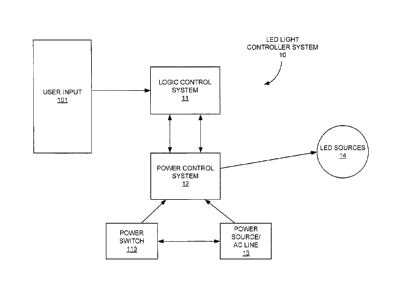
[0007] FIG. 1 is a schematic illustration of a LED light controller system
according
to one embodiment of the disclosure.
[0008] FIG. 2 is a schematic illustration of a logic control system for use
with the
LED light controller system of FIG. 1.
[0009] FIG. 3 is a schematic illustration of a user input for use with the
logic control
system of FIG. 2.
[0010] FIG. 4 is a schematic illustration of a switch data acquisition for
use with the
logic control system of FIG. 2.
[0011] FIG. 5 is a schematic illustration of switch indicators for use with
the logic
control system of FIG. 2.
[0012] FIG. 6 is a schematic illustration of a programming port for use
with the logic
control system of FIG. 2.
[0013] FIG. 7 is a schematic illustration of a microcontroller circuit for
use with the
logic control system of FIG. 2.
[0014] FIG. 8 is a schematic illustration of a comparator circuit for use
with the logic
control system of FIG. 2.
CA 02703933 2010-04-23
WO 2009/058297
PCT/US2008/012266
3
[0015] FIG. 9
is a schematic illustration of a control logic for use with the logic control
system of FIG. 2.
[0016] FIG. 10
is a schematic illustration of a connection block for use with the logic
control system of FIG. 2.
[0017] FIG. 11
is a schematic illustration of a power control system for use with the LED
light controller system of FIG. 1.
[0018] FIG. 12
is a schematic illustration of an optoisolator for use with the power
control system of FIG. 11.
[0019] FIG. 13
is a schematic illustration of a triac circuit for use with the power control
system of FIG. 11.
[0020] FIG. 14
is a schematic illustration of a power switch for use with the power
control system of FIG. 11.
[0021] FIG. 15
is a schematic illustration of a transformer, a rectifier, and a regulator for
use with the power control system of FIG. 11.
[0022] FIG. 16
is a schematic illustration of a zero-crossing detection circuit for use with
the logic control system of FIG. 2.
[0023] FIG. 17
is a schematic illustration of a current sensing circuit for use with the
power control system of FIG. 11.
[0024] FIG. 18
is a flow chart illustrating operation of the LED light controller system of
FIG. 1.
[0025] FIGS.
19A-19C are different views of physical embodiments of the LED light
controller system of FIG. 1.
[0026] FIG. 20
is a wiring diagram of the LED light controller system of FIG. 1
according to some embodiments of the disclosure.
CA 02703933 2010-04-23
WO 2009/058297
PCT/US2008/012266
4
DETAILED DESCRIPTION
[0027] Before
any embodiments of the disclosure are explained in detail, it is to be
understood that the disclosure is not limited in its application to the
details of construction
and the arrangement of components set forth in the following description or
illustrated in the
following drawings. The disclosure is capable of other embodiments and of
being practiced
or of being carried out in various ways. Also, it is to be understood that the
phraseology and
terminology used herein is for the purpose of description and should not be
regarded as
limiting. The use of "including," "comprising," or "having" and variations
thereof herein is
meant to encompass the items listed thereafter and equivalents thereof as well
as additional
items. Unless
specified or limited otherwise, the terms "mounted," "connected,"
"supported," and "coupled" and variations thereof are used broadly and
encompass both
direct and indirect mountings, connections, supports, and couplings, whether
mechanical or
electrical. Further, "connected" and "coupled" are not restricted to physical
or mechanical
connections or couplings.
[0028] In
addition, it should be understood that embodiments of the invention include
both hardware and electronic components or modules that, for purposes of
discussion, may be
illustrated and described as if the majority of the components were
implemented solely in
hardware. However, one of ordinary skill in the art, and based on a reading of
this detailed
description, would recognize that, in at least one embodiment, the electronic
based aspects of
the invention may be implemented in software. As such, it should be noted that
a plurality of
hardware and software based devices, as well as a plurality of different
structural components
may be utilized to implement the invention. Furthermore, and as described in
subsequent
paragraphs, the specific mechanical configurations illustrated in the drawings
are intended to
exemplify embodiments of the invention and that other alternative mechanical
configurations
are possible.
[0029] FIG. 1
illustrates a schematic of a light emitting diode (LED) light controller
system 10 according to one embodiment of the disclosure. An enclosure
containing circuit
boards as well as push buttons and a rotary switch for a user can be mounted
on a wall of a
standard outlet/switch box. The box can be metal or plastic. A multitude of
color shows can
be represented on an overlay of the enclosure. The user can align the rotary
switch to a
specific color show representation on the overlay. The LED light controller
system can read
CA 02703933 2010-04-23
WO 2009/058297
PCT/US2008/012266
this selection from the user and output the specific color show by controlling
LEDs in pool,
spa, and/or landscape lights or sources.
[0030] The
controller system 10 can include a user input 101 and a power switch 110, a
logic control system 11, a power control system 12, an AC power source (e.g.,
AC mains
line) 13, and LED sources 14. In one embodiment, these components can be
connected as
shown by arrows in FIG. 1; however, other configurations are possible. The LED
sources 14
can include LED pool, spa, and/or landscape lights, or any other LED sources
capable of light
output control in the form of fixed-color or multi-colored shows. The LED
sources 14 can be
a multitude of different color LEDs. The LED sources 14 can be 120 volt (V)
lights or 12V
lights including a step-down transformer. The AC line 13 can be connected to
the power
control system 12 through a ground fault circuit interrupter (GFCI) as the
source of power to
a portion of the entire LED light controller system 10, including the power
control system 12,
the logic control system 11, and the LED sources 14. In addition, the power
switch 110 can
be connected to the power control system 12 to selectively provide or remove
power to the
LED light controller system 10. If the LED light controller system 10 is on
(e.g., the power
switch 110 is enabled), specific color show information from the user input
101 can be
received and processed by the logic control system 11. The logic control
system 11 can then
output specific voltage pulses to signal the power control system 12 to clip
or truncate the AC
line 13 supplied to the LED sources 14. The specific number of AC line
truncations
(equating to the number of output pulses) can be interpreted by decode
circuitry in the LED
sources 14. As a result, the single LEDs within the LED sources 14 can be
turned on or off to
output various colors of the color show selected by the user.
[0031] FIG. 2
illustrates the logic control system 11 of the LED light controller system 10
according to one embodiment of the disclosure. The logic control system 11 can
include the
user input 101, a switch data acquisition circuit 102, a microcontroller
circuit 103, a
reprogramming port 104, a comparator 105, switch indicators 106, an output
control logic
107, a zero-crossover detection circuit 108, and a connection block 109. The
connection
block 109 can serve as the connection between the logic control system 11 and
the power
control system 12. The components of the logic control system 11 can be
integrated circuits
mounted on a circuit board that is positioned within the enclosure.
CA 02703933 2010-04-23
WO 2009/058297
PCT/US2008/012266
6
[0032] FIG.
3 further illustrates the user input 101 from the logic control system 11 of
FIG. 2. The user input 101 can include a rotary switch 135, a recall
button/switch 136, and a
- hold button/switch 137. The rotary switch 135 can be a continuous, 12-
position switch, such
as those manufactured by C&K Components. The rotary switch 135 can be aligned
on the
front panel of the enclosure. The front panel can also include an overlay
corresponding to a
multitude of fixed-color or multi-colored show selections relative to the
position of the rotary
switch 135. From the rotary switch 135, the color show selection information
can be sent to
shift registers 138, 139 within the switch data acquisition circuit 102 (as
shown in FIG. 4) via
connection 122. In some embodiments, the rotary switch 135 can be replaced by
an encoder
or potentiometer. The encoder or potentiometer can perform the same function
as the rotary
switch 135 by transmitting a different signal for a different chosen selection
without the
requirement of a multitude of wires for the connection 122. The recall switch
136 and the
hold switch 137 can be single-pole, single-throw (SPST) tactile switches, such
as the
MJTP1138B, manufactured by APEM. If the recall switch 136 is depressed, its
two
terminals can connect to ground and a low voltage signal can be received by
the
microcontroller circuit 103 (as shown in FIG. 3) via connection 123. If the
hold switch 137 is
depressed, the microcontroller circuit 103 can receive a signal via connection
124.
[0033] FIG.
4 illustrates the switch data acquisition circuit 102 of the logic control
system
11. The switch data acquisition block 102 can contain two shift registers 138,
139 and a
resistor network 146 (including resistors R1-R12) to provide decoded rotary
switch position
information to the microcontroller circuit 103. The two shift registers 138,
139 can be 8-bit
parallel-in/serial-out shift registers, such as the 74HC165D, manufactured by
NXP
Semiconductors. The resistance of the resistors R1-R12 can be equal to one
another and can
be 10 kilo-ohms (these resistors as well as all resistors described herein can
be 0805 size with
a power rating of 1/8 watts). Specific bit patterns based on the position of
the rotary switch
135 can be routed to the microcontroller circuit 103 via a connection 125. A
connection 128
from the microcontroller circuit 103 can provide an interrupt to call for data
("LD") from the
shift registers 138, 139. Additionally, clock information ("CLK") for the
shift registers 138,
139 can come from the microcontroller circuit 103 via a connection 129.
[0034] When
either the hold or recall function is in use, the microcontroller circuit 103
can trigger a visible LED to show the active function to the user. As shown in
the switch
CA 02703933 2010-04-23
WO 2009/058297
PCT/US2008/012266
7
indicator block 106 in FIG. 5, visible LEDs D1 and D2 can be connected in
series with
resistors R13 and R14, respectively, and a supply voltage, Vcc (e.g., 5
volts). LEDs D1 and
D2 can be SOT-23 surface mount 635 nm red LEDs, such as those manufactured by
LUMEX
(part number SSL-LS151C-TR). Resistors R13 and R14 can each be 470 ohms in
some
embodiments. The resistors R13 and R14 act as current limiters, and the value
of resistors
R13 and R14 can vary depending on the type of diode used. A low output from
the
microcontroller circuit 103 (via connections 126 and 127) can allow a
sufficient voltage drop
to activate either diode to signal to the user which function is in use (e.g.,
whether the recall
switch 136 or the hold switch 137 has been depressed). LEDs D1 and D2 can be
mounted so
that they are visible to the user on the front panel of the enclosure.
[0035] FIG. 6
illustrates the reprogramming port 104. The reprogramming port 104 can
allow reprogramming of a microcontroller 141 (as shown in FIG. 7) within the
microcontroller circuit 103 once the LED light controller system 10 is already
installed in the
enclosure. The reprogramming port 104 can be directly connected to the
microcontroller
circuit 103 via connections 132 (pin 3) and 134 (pin 4) to synchronize system
clocks and send
data, respectively. A supply voltage, VDD can be supplied to the
microcontroller 141 (at pin
2) by the power control system 12 during normal operation. During
reprogramming,
however, power can be removed from the LED light controller system 10 and,
therefore, VDD
will no longer be supplied to the microcontroller circuit 103. In this case,
VDD, can be
supplied to the microcontroller 141 by the reprogramming port 104 via a
connection 140. In
addition, a higher voltage Vpp can be supplied from the reprogramming port 104
(at pin 5) via
a connection 124 to the microcontroller circuit 103 to put the microcontroller
141 into a
programming mode.
[0036] FIG. 7
further illustrates the microcontroller circuit 103 included in the logic
control system 11. In some embodiments, the microcontroller 141 included in
the
microcontroller circuit 103 can be a PIC16F684 (14-pin flash-based, 8-bit
CMOS)
manufactured by Microchip Technology, Inc. or similar. As used herein and in
the appended
claims, the term "microcontroller" is not limited to just those integrated
circuits referred to in
the art as microcontrollers, but broadly refers to one or more microcomputers,
processors,
application-specific integrated circuits, or any other suitable programmable
circuit or
combination of circuits. Pin 1 of the microcontroller 141 can be connected to
the voltage
CA 02703933 2010-04-23
WO 2009/058297
PCT/US2008/012266
8
source VDD to power the device during normal operation, while pin 14 can be
grounded. The
voltage source VDD can have a transient protection circuit at pin 1. The
transient circuit can
contain a schottky diode D3 and a capacitor Cl in series connection with
supply voltage Vcc.
The diode D3 can be a SMA 8360A-13, manufactured by Diodes, Inc. The capacitor
Cl can
be a 0.1 microfarad ( 10%), size 0805, X7R dielectric type capacitor rated for
25V, such as
that manufactured by AVX Corporation (Part No. 08053C104KAT2A). Unless
specified
otherwise, all the capacitors described herein can be this type of capacitor.
[0037] Due to
a large amount of inputs and outputs, pins of the microcontroller 141 can
be shared using jumpers 142. As shown in FIG. 7, pins 12 and 13 of the
microcontroller 141
have two separate wire connections, 132 and 133, and 134 and 127,
respectively, coming into
the microcontroller circuit block 103. During reprogramming of the
microcontroller 141 with
the reprogramming port 104, the jumpers 142 can be disconnected to allow the
connection of
pins 12 and 13 to the connections 132 and 134, respectively. Otherwise, the
jumpers 142 can
be connected to allow the connection of pins 12 and 13 to the connections 133
and 127,
respectively, for normal operation.
[0038] The
output from the microcontroller 141 to control the action of the LED sources
14 can be provided via pins 8 and 12 through the connections 130 and 133. The
microcontroller 141 can be connected to the recall switch 136 (at pin 2) and
the hold switch
137 (at pin 4) from the user input 101 via the connections 123 and 124,
respectively. When
the hold switch 137 is depressed, the microcontroller 141 can control the
output signal (at
pins 8 and 12) to hold the color that is currently showing at that time. This
signal information
can also be stored in the microcontroller 141 for use during the recall switch
136 operation.
When the recall switch 136 is depressed, the microcontroller 141 can control
the LED
sources 14 to output the last color stored during the hold button 138
operation. The
microcontroller 141 can include an internal pull-up resistor for the switches
(at pin 2) or can
use an external pull-up resistor (e.g., a resistor R31 in series with Vcc at
pin 4) for the recall
switch 136 and the hold switch 137. In some embodiments, the resistor R31 can
be 10 kilo-
ohms.
[0039] In
addition, data from the switch data acquisition circuit 102 can be input to
the
microcontroller 141 (at pin 3) via the connection 125. The microcontroller 141
can provide a
signal (at pin 7) to the shift registers 138, 139 to call for data via the
connection 129. The
CA 02703933 2010-04-23
WO 2009/058297
PCT/US2008/012266
9
internal clock of the microcontroller 141 (output at pin 6) can be used by the
shift registers
138, 139 in the switch data acquisition circuit 102 through the connection
128. The
microcontroller 141 can also output signals to the switch indicators 106 via
connections 126
and 127 from pins 5 and 13, respectively.
[0040] Two
pins of the microcontroller 141 (e.g., pins 9 and 10) can be used for the
comparator circuit 105, as shown in FIG. 8. Pin 9 can receive a reference
voltage from the
comparator circuit 105 via the connection 131, while pin 10 can receive a
current sense
voltage from the power control system 12 via the connection 119. Also, the
zero-crossover
detection circuit 108 (as shown in FIG. 16) can communicate the zero-crossover
of the AC
line 13 to the microcontroller 141 via the connection 143 at pin 11 (as
further discussed with
respect to the power control system 12).
[0041] A
safety mechanism including output current detection can be included in some
embodiments. The magnetic field of the final output power trace can be
detected, converted
to a respective current sense voltage, and fed back to the microcontroller
141. In response to
the input voltage, the microcontroller 141 can then be capable of providing or
removing ,
output power to the LED sources 14. This can prevent too much current from
reaching the
LED sources 14 if any connections prior to the output trace are shorted or
overloaded during
startup (in addition to a fuse F1, as shown in FIG. 13). The current sense
voltage from the
power control system 12 can be routed to the microcontroller 141 via the
connection 119.
[0042] The
comparator circuit 105 (as shown in FIG. 8) can be connected to the
microcontroller circuit 103 via the connection 131. The comparator circuit 105
can use a
voltage divider with resisters R15 and R16, capacitor C2, and supply voltage
Vcc to produce
a reference voltage; the magnitude of this reference voltage can be the
threshold for the
current sense voltage from the power control system 12 (i.e., a voltage trip
point). In some
embodiments, resistor R15 can have a resistance of 15 kilo-ohms and resistor
R16 can have a
resistance of 51 kilo-ohms, while capacitor C2 can have a 0.1 microfarad
capacitance.
Therefore, by way of example only, if the supply voltage Vcc is about 5V, then
the reference
voltage at the connection 131 can be about IV. The input to the
microcontroller 141 from the
current sense voltage (at the connection 119) can be compared to the reference
voltage (at the
connection 131). If the detected current sense voltage is above the voltage
trip point, the ,
microcontroller 141 can shut down its output, thus removing power to the LED
sources 14.
CA 02703933 2010-04-23
WO 2009/058297
PCT/US2008/012266
[0043] To
ensure proper microcontroller 141 operation, two pins on the microcontroller
141 (pins 8 and 12 as shown in FIG. 7) can provide output signals in the form
of voltage
pulses to the power control system 12. The output of these two pins can be
sent to the control
logic 107 (as shown in FIG. 9) via the connections 130 and 133, respectively.
As shown in
FIG. 9, the two outputs from the microcontroller circuit 103 can be fed
through logic gates to
ensure consistency before being output to the power control system 12. Logic
NOR gates
G 1, G2 (e.g., model 74HCO2/SO, available from several manufacturers) can be
used, in some
embodiments. In alternative embodiments, other logic gates can be used and
configured for
the same purpose of qualifying correct output before sending information to
the power
control system 12. Resistors R17, R18, and R20 in the control logic 107 can
have a
resistance of 10 kilo-ohms while resistor R19 can have a resistance of 4.7
kilo-ohms.
Transistor Q1 can be a PMBT3904 BJT, manufactured by Phillips, among others.
If the
microcontroller 141 is not transmitting any signals from pins 8 and 12, the
pull-down resistor
R17 in connection with ground can drive the connection 130 low, while the pull-
up resistor
R18 in connection with Vcc can drive the connection 133 high. The low-driven
voltage at
connection 130 can allow a high logic level voltage (e.g., Vcc or 5V) emitted
from GI. The
combination of high logic level voltage from G1 and high-driven voltage from
the connection
133 can cause a low logic level (e.g., OV) to be emitted from G2; therefore,
no signal will be
sent to the power control system 12. When a user input has been detected, the
microcontroller 141 can emit a high voltage (5V) pulse at (pin 8) and a
simultaneous low
voltage (OV) pulse (at pin 12), resulting in a high logic level (5V) at the
output of G2. Each
pulse output from the microcontroller 141 (qualified by the logic control 107)
can allow the
transmission of the high logic level emitted from G2 through a voltage divider
including
resistors R19 and R20. The voltage after the resistor R19 can surpass the cut-
in voltage
needed at the base of the transistor Q 1 to operate the transistor Q1 in an
active mode,
allowing current to flow from the transistor's collector (at the connection
121) through its
emitter to ground.
[0044] The
final signal from the control logic 107 can be provided to the power control
system 12 via the connection 121 to connection block 109, as shown in FIG. 10.
The
connection block 109 can provide communication between the power control
system 12 and
the logic control system 11. The connection block 109 can be a printed circuit
board (PCB)
connector. As shown in FIG. 10, eight pins on the connection block 109 can
transmit four
CA 02703933 2010-04-23
WO 2009/058297
PCT/US2008/012266
11
different signals between the logic control system 11 and the power control
system 12. The
other two pins on each side can be grounded. Output signals from the control
logic 107 of
the logic control system 11 (at the connection 121) can be routed to the power
control system
12 as the connection 144. Current sense information received by the logic
control system 11
(at the connection 119) can be routed from the power control system 12 as the
connection
145. The rectified, stepped-down voltage Vcc that can power the
microcontroller 141, shift
registers 138, 139, rotary switch 136, and other equipment of the logic
control system 10 can
be routed from the connection 146 of the power control system 12 to the
connection 118 of
the logic control system 11. A bypass capacitor C3 can also be connected to
the connection
118. The capacitor C3 can be a 220 microfarad ( 10%), tantalum electrolytic
capacitor rated
for 10V, such as that manufactured by Nichicon Corporation (Part No.
UWX1A221MCLIGB). Another rectified voltage (not stepped-down to the magnitude
of
Vcc) can be connected from the power control system 12 (at the connection 147)
to the logic
control system 11 (at the connection 120) for the zero-crossover detection
block 108 (as
shown in FIG. 16).
[0045] FIG. 11
illustrates the power control system 12 of the LED light controller system
according to one embodiment of the disclosure. The power control system 12 can
include
the power switch 110, an AC connections block 111, a transformer 112, a
rectifier 113, a
voltage regulator 114, an opto-isolator 115, a triac circuit 116, current
sensing circuitry 117,
and the connection block 109. The components of the power control system 12
can be
integrated circuits mounted on a circuit board that is positioned within the
enclosure.
[0046] As
shown in FIG. 12, the opto-isolator 115 can provide an interface between the
logic control system 11 and the triac circuit 116, in some embodiments. A
photodiode D4
can be connected in series with a resistor R21 and voltage supply Vcc. In some
embodiments, the resistor R21 can be 220 ohms. The active mode operation from
the
transistor Q1 in the control logic 107 via the connection 144 can pull current
through the
resistor R21, causing the photodiode D4 to turn on. Light output from the
photodiode D4
can, in turn, trigger operation of the triac Ti. Current through the triac T1
(via the
connections 148 and 149) can then activate the triac circuit 116 (as shown in
FIG. 13). The
opto-isolator 115 used in some embodiments (including the photodiode D4 and
the triac T1)
can be model MOC3021M, manufactured by Fairchild Optoelectronics Group, among
others.
CA 02703933 2010-04-23
WO 2009/058297
PCT/US2008/012266
12
Similar isolation circuits to isolate the low voltage microcontroller circuit
from the high
mains voltage can be used in other embodiments.
[0047] FIG. 13
further illustrates the triac circuit 116 of the power control system 12. A
triac T2 (or similar AC switching device) can clip or truncate the AC line 13
(from the
connection 151) to the LED sources 14 (via the connection 150) in response to
the signals (or
lack thereof) received from the triac T1 of the opto-isolator circuit 115 (at
the connection
149). As shown in FIG. 13, the connection 149 from the opto-isolator 115 can
apply current
to the gate of the triac T2 to trigger current through the triac T2 in either
direction (through
the connection 151 to the connection 150 or vice-versa), thus providing full
mains voltage
(e.g., 120 VAC) to the LED sources 14. A resistor R24 (e.g., 39 ohms) and a
capacitor C4
(e.g., 0.01 microfarads) can act as an RC filter to prevent large spikes in
voltage in the case of
a current interruption. Resistors R22 (e.g., 470 ohms) and R23 (e.g., 360
ohms) can provide
current limiting and a voltage divider for the triac T2. A capacitor C5 (e.g.,
0.047
microfarads) can filter out any spikes that can occur when the triac T2 is
turned on. Resistors
R22, R23, and R24 can have a 1/4-watt power rating. The triac circuit can
further include fuse
Fl (e.g., a slow-blow, long-time lag, 7-amp fuse such as a 0473007.YRT1,
manufactured by
Littelftise, Inc.) to prevent current overload to the LED sources 14. The use
of the triac
circuit 116 enables the voltage source provided to the LED sources 14 to be
truncated (e.g.,
clipped) rather than completely deactivated (e.g., toggled on/off).
[0048] AC
power to the LED light controller system 10 can be controlled via the power
switch 110. FIG. 14 illustrates the power switch 110 according to one
embodiment of the
disclosure. The power switch 110 can be a normally-open contact switch that
can provide or
remove power to or from the LED light controller system 10. The power switch
110 can be a
water-proof pushbutton switch (such as the LA series switches manufactured by
E-Switch)
connected to the power control circuit 12 by a switch connector assembly. The
power switch
110 can also include an indicator light 158, as shown in FIG. 14. The power
switch 110 can
be connected to the transformer 112 (via the connections 154 and 153) and the
AC
connections block (via the connections 152 and 154) to allow power from the AC
line 13 to
be provided through the power control system 12 to the LED sources 14.
[0049] As
shown in FIG. 15, the step down transformer 112 can provide low voltage
from the full AC supply 13 for the bridge rectifier 113 and the voltage
regulator 114. The
CA 02703933 2010-04-23
WO 2009/058297
PCT/US2008/012266
13
transformer 112 can be a single 10VAc, 0.5-amp power transformer, such as
model 3FS-310,
manufactured by Tamura. The rectifier 113 can be a 1A, DIL bridge rectifier,
such as model
DFO2S manufactured by Fairchild Semiconductors, among others. The voltage
regulator 114
can be a 3-terminal, 0.1-amp, positive voltage regulator, such as the
LM78L05A,
manufactured by Fairchild Semiconductors. The power supply to the transformer
112 can
come from the connection 154 (which is further connected to the AC connections
block 109)
and the connection 153 (which is further connected to the connection 151 of
the triac circuit
116). If the power switch 110 is off, there can be no AC voltage through the
connection 153
and therefore the transformer 112 can not be in operation, and thus no power
can be supplied
to the LED light controller system 10. The output voltage from the bridge
rectifier 113 (via
the connection 147) can supply a rectified DC voltage to the logic control
system 11. From
the connection 147 through the connection block 109 to the connection 120, the
rectified DC
voltage can be supplied to the zero-crossover detection circuit 108. The
connection 153/151
can further lead to the triac circuit 116 and can include a fuse F2 (e.g., a
fast-acting, short-
time lag, 3-amp fuse such as a 6125FA, manufactured by Cooper/Bussmann) to
prevent
current overload.
[0050] Also
included before and after the voltage regulator 114 can be transient and
reverse-voltage protection circuitry, such as a diode D9 and capacitors C6-C8.
The diode D9
can be a SMA B360A-13, manufactured by Diodes, Inc. In some embodiments, the
capacitors C6, C7, and C8 can have a capacitance of 0.1 microfarads, 0.01
microfarads, and
0.33 microfarads, respectively. The output from the voltage regulator 114 can
supply the
stepped-down, rectified voltage Vcc to components of both the power control
system 12 and
the logic control system 11. The voltage Vcc can be supplied to the logic
control system 11
via the connection 146 through the connection block 109 to the connection 118.
[0051] FIG. 16
illustrates the zero crossover detection circuit 108. The zero crossover
detection circuit 108 can include resistors R25-R27 and a transistor Q2.
Resistors R25, R26,
and R27 can have resistances of 4.7 kilo-ohms, 1.0 kilo-ohms, and 10 kilo-
ohms,
respectively. The transistor Q2 can be a PMBT3904 BJT, manufactured by
Phillips, among
others. The rectified DC voltage supplied to the zero crossover detection
circuit 108 (via the
connection 120) of the logic control system 11 can allow the microcontroller
141 to
synchronize with the AC line 13. This voltage to the transistor Q2 (via the
connection 120 at
CA 02703933 2010-04-23
WO 2009/058297
PCT/US2008/012266
14
the base of the transistor Q2) drops to zero volts when the AC line amplitude
crosses zero
volts. The zero-volt base input can turn on the transistor Q2 in an active
mode which in turn
can pull the respective input to the microcontroller circuit 103 low (via the
connection 143
from the collector of the transistor Q2). The low input signal representing
zero crossover of
the AC line 13 can then synchronize the microcontroller 141 to the AC line 13.
This can
provide the proper timing for the microcontroller 141 to switch the triac T2,
thus reducing the
chances for spiking.
[0052]
Referring back to the power control system 12, the final clipped AC signal
from
the triac T2 (at the connection 150) can be routed to the AC connections block
111, which
can power the LED sources 14, producing the desired light output. The current
sensing
circuit 117 can be placed on one side of the power control system circuit
board opposite the
output power trace at the connection 150 (i.e., above or below the trace) and
can include, as
shown in FIG. 17, a current sensing device 155 and an amplifying circuit 156.
The current --
sensing device 155 can be an integrated magnetic field sensor, such as the CSA-
1V, in a
SOIC-8 package, manufactured by GMW. A ferrite bead (not shown) can be placed
on the
trace near the current sensing device 155, helping amplify the magnetic field.
The current
sensing device 155 can convert the magnetic energy from the output trace (at
the connection
150) to a voltage proportional to the current through the output trace.
[0053] As
shown in FIG. 17, the voltage signal from the current sensing device 155 (at
the connection 157) can be amplified and filtered via the amplifying circuit
156. The
amplifying circuit 156 can include resistors R28-R30, capacitor C10, and an op
amp Al. The
op amp Al can be a single CMOS op amp with low-voltage, low-power, and rail-to-
rail
output swing capabilities in an SOT-23 package, such as the TLV341 model
(TLV341IDBVR), manufactured by Texas Instruments. In some embodiments, the
resistor
- R28 can be 10 kilo-ohms, the resistor R29 can be 82.5 kilo-ohms, and
the resistor R30 can be
18 kilo-ohms. Capacitors C9 (e.g., 1 microfarad), C10 (e.g., 100 picofarads),
and C11 (e.g.,
0.1 microfarads) can provide transient protection for the current sensing
circuit 117. The
current sense voltage output by the amplifying circuit 156 can be routed to
the connection
block 109 (via the connection 145). The current sense voltage from the
connection block 109
(at the connection 119 in the logic control system 11) can be routed to the
microcontroller
circuit 103. As previously discussed, if detected current sense voltage is
above the voltage
CA 02703933 2010-04-23
WO 2009/058297
PCT/US2008/012266
trip point, the microcontroller 141 can shut down its output, thus removing
power from the
LED sources 14. In addition, the microcontroller 141 can flash the diodes D1
and D2 of the
switch indicator block 106 if detected current is above the voltage trip point
to alert the user
that a problem has occurred. The AC connections block 111 (as shown in FIG.
11) can
accommodate voltage connections between the AC line 13, the power control
system 12, and
the LED sources 14.
[0054] FIG. 18
illustrates a flow chart 200 describing portions of the operation of the
LED light controller system 10, according to some embodiments. First, the user
input 101 is
activated (task 201). Activating the user input can include pressing of the
hold switch 137,
pressing of the recall switch 136, or rotating the rotary switch 135 to a
selected color show.
Depending on which switch is activated, different paths of operation can be
taken (task 202).
If the hold switch 137 is depressed, the microcontroller 141 determines the
current output
color of the LED sources 14 (task 203) and activates the hold switch indicator
106 (task 204).
If the recall switch 136 is depressed, the microcontroller 141 determines the
output color held
during the last hold switch operation (task 205) and activates the recall
switch indicator 106
(task 206). If the rotary switch 135 is adjusted, the switch data acquisition
102 interprets the
rotary switch position and creates a bit pattern specific to that position
(task 207). The
microcontroller 141 then interprets the bit pattern created by the switch data
acquisition 102
as a specific color show (task 208). After task 203, task 205, or task 208,
the microcontroller
141 outputs a specific number of output voltage pulses to the control logic
107 (task 209).
The control logic 107 validates the microcontroller 141 operation (task 210).
Task 210 will
continue to loop back to task 209 until the control logic 107 validates proper
output. Once
correctly validated, the control logic 107 outputs the output voltage pulses
to activate the
opto-isolator 115 (task 211). The opto-isolator 115 activates the triac
circuit 116 with the
pulsed voltage output (task 212). The pulsed voltage output turns on the triac
circuit 116 in
pulses and truncates the AC line 13 to the LED sources 14 (task 213). The LED
sources 14
interpret the specific number of pulses and output a respective color show
(task 214).
[0055] Also
shown in FIG. 18 is a sub-flow chart 300 of the current sensing circuit 117,
acting as an interrupt to the microcontroller 141. The current sensing circuit
117 senses the
current of the output trace at the connection 150 (task 301). The current
sensing circuit 117
transmits the current sense voltage proportional to the current of the output
trace to the
CA 02703933 2010-04-23
WO 2009/058297
PCT/US2008/012266
16
microcontroller 141 (task 302). The microcontroller 141 sends the current
sense voltage to
the comparator 105 (task 303). The comparator 105 compares the current sense
voltage to
the threshold voltage (task 304). If the current sense voltage is below the
threshold voltage,
the microcontroller 141 will continue to provide output the LED sources 14
(task 305). If the
current sense voltage is greater than the threshold voltage, the
microcontroller 141 will shut
down its output to remove power from the LED sources 14 and flash the diodes
D1 and D2 of
the switch indicator block 106 (task 306).
[0056] FIGS.
19A-19C illustrate the LED light controller system 10 according to some
embodiments of the disclosure. The LED light controller system 10 can include
a front cover
400 and a rear cover 401. The front cover 400 can be coupled to the rear cover
by fasteners
403 (e.g., screws) to form an enclosure. A circuit assembly 402 can be housed
within the
enclosure. The circuit assembly 402 can include the logic control system 11
and the power
control system 12. The circuit assembly 402 can also include the recall switch
136, the hold
switch 137, the rotary switch 135, and the power switch 110. The front cover
400 can
include holes 404 to permit the rotary switch 135 and the power switch 110 to
extend out past
the front cover 400. An overlay 405 can be coupled to the front of the front
cover 400. The
overlay 405 can include images representing color shows to allow a user to
position the
rotary switch 135 to select a desired color show. The front cover 400 can also
include
notches 406 that, when depressed, can actuate either the recall switch 136 or
the hold switch
137. The overlay 405 can also include indicators positioned over the notches
406
representing the recall switch and the hold switch. The overlay 405 can be
made of
substantially thin material such the pressing the indicator will depress one
of the notches 406
and therefore actuate the recall switch 136 or the hold switch 137. A door 407
can be
coupled to the front cover 400 and can cover the overlay 405 and the rotary
switch 135. The
door 406 can include a door hole 407. The door hole 408 can be positioned so
that a user can
access the power switch 110 when the door 407 is closed. Labels 409 can be
included on the
inside of the door 407 and on the backside of the rear cover 401. The front
cover 400 can be
coupled to a gasket 410. The gasket 410 can be mounted to a outlet/switch box
with fasteners
411 (e.g., screws). The AC connections 111 can extend outside the rear cover
401 and can be
connected to the LED sources 14 and the AC source 13.
CA 02703933 2010-04-23
WO 2009/058297
PCT/US2008/012266
17
[0057] FIG. 20
illustrates a wiring diagram for the LED light controller system 10
according to some embodiments of the disclosure. The LED light controller
system 10 can
be housed within a metal gang box 412. The front cover 400 of the LED light
controller
system 10 can permit access to the power switch 110 to control power to the
LED light
controller system 10. The power switch 110 can be connected to the power
control system
12. The power control system 12 can receive power from a ground fault circuit
interrupter
(GFCI) 413. Power to the GFCI 413 can come from the AC power source (AC line)
13.
Wire connections can be protected by a rigid or PVC conduit 414. The power
control system
12 can be connected to the plurality of LED sources 14 via a junction box 415.
The plurality
of LED sources 14 can include landscape, pool, and/or spa lights. Once the
power switch
110 has been depressed, a "hot" voltage wire from the GFCI 413 can be in
connection with
the "switched hot" voltage wire, thus providing voltage to the plurality of
LED sources 14.
The power control system 12 can clip the AC voltage on the "switched hot"
voltage wire to
provide pulses to the plurality of LED sources 14. Decode circuitry within the
plurality of
LED sources 14 can process the number of pulses received and output a
corresponding light
show. The number of pulses provided can determined by the logic control system
11 (not
shown) from the user input 101 (not shown).
[0058] It will
be appreciated by those skilled in the art that while the disclosure has been
described above in connection with particular embodiments and examples, the
disclosure is
not necessarily so limited, and that numerous other embodiments, examples,
uses,
modifications and departures from the embodiments, examples and uses are
intended to be
encompassed by the claims attached hereto. Various features and advantages of
the
disclosure are set forth in the following claims.