Note: Descriptions are shown in the official language in which they were submitted.
CA 02704304 2014-01-24
BIOPOLYMER OPTICAL WAVEGUIDE AND
METHOD OF MANUFACTURING THE SAME
BACKGROUND OF THE INVENTION
Field of the Invention
[0003] The present invention is directed to biopolymer optical waveguides
and
methods for manufacturing such devices.
Description of Related Art
[0004] The field of optics is well established. Some subfields of optics
include
diffractive optics, micro-optics, photonics and guided wave optics. Various
optical
devices have been fabricated in these and other subfields of optics for
research and
commercial application. For example, common optical devices include
diffraction
gratings, photonic crystals, optofluidic devices, waveguides, and the like.
[0005] Optical waveguides are physical structures that guide
electromagnetic
waves in the optical spectrum. Common types of optical waveguides include
optical
fiber and rectangular waveguides. Optical waveguides are often used as
components
in integrated optical circuits or as the transmission medium in optical
communication
systems. Optical waveguides may be classified according to their geometry,
such as
planar, strip, or fiber waveguides. They may also be classified according to
their
mode structure, such as single-mode or multi-mode. Likewise, optical
waveguides
-1-
CA 02704304 2010-04-30
WO 2008/127401
PCT/US2007/083605
may be categorized according to their refractive index distribution, such as
step or
gradient index. Additionally, optical waveguides may also be classified
according to
their material composition, such as glass, semiconductor, or polymer.
[0006] These optical devices are fabricated using various methods depending
on
the application and optical characteristics desired. However, these optical
devices,
and the fabrication methods employed in their manufacture, generally involve
significant use of non-biodegradable materials. For example, glass, fused
silica, and
plastic are commonly used in optical devices. Such materials are not
biodegradable
and remain in the environment for extended periods of time after the optical
devices
are removed from service and discarded. Of course, some of the materials can
be
recycled and reused. However, recycling also requires expenditures of natural
resources, and adds to the environmental costs associated with such materials.
[0007] Therefore, there exists an unfulfilled need for optical waveguides
that
minimize the negative impact to the environment. In addition, there exists an
unfulfilled need for optical waveguides that provide additional functional
features that
are not provided by conventional optical waveguides.
SUMMARY OF THE INVENTION
[0008] In view of the foregoing, objects of the present invention are to
provide
novel biopolymer optical waveguides and methods for manufacturing such optical
waveguides that may be used in various applications.
[0009] One aspect of the present invention is to provide biopolymer
waveguide
devices.
[0010] Another aspect of the present invention is to provide a method for
manufacturing such biopolymer waveguide devices.
[0011] One advantage of the present invention is in providing biopolymer
waveguide devices that minimize the negative impact to the environment.
[0012] Another advantage of the present invention is in providing
biopolymer
waveguide devices that are biocompatible.
-2-
CA 02704304 2010-04-30
WO 2008/127401
PCT/US2007/083605
[0013] Yet another advantage of the present invention is in providing
biopolymer
waveguide devices that have additional functional features that are not
provided by
conventional optical waveguides.
[0014] In the above regard, inventors of the present invention recognized
that
biopolymers, and especially silk proteins, present novel structure and
resulting
functions. For example, from a materials science perspective, silks spun by
spiders
and silkworms represent the strongest and toughest natural fibers known and
present
various opportunities for functionalization, processing, and biocompatibility.
Over
five millennia of history accompany the journey of silk from a sought-after
textile to a
scientifically attractive fiber. As much as its features had captivated people
in the
past, silk commands considerable attention in this day and age because of its
strength,
elasticity, and biochemical properties. The novel material features of silks
have
recently been extended due to insights into self-assembly and the role of
water in
assembly. These insights, in turn, have led to new processing methods to
generate
hydrogels, ultrathin films, thick films, conformal coatings, three-dimensional
porous
matrices, solid blocks, nanoscale diameter fibers, and large diameter fibers.
[0015] Silk-based materials achieve their impressive mechanical properties
with
natural physical crosslinks of thermodynamically stable protein secondary
structures
also known as beta sheets (I3-sheets). The high number of nanoscale aligned
crystals
(I3-sheets), combined with highly hydrogen bonded, less crystalline domains
leads to a
unique structure and functional features. No exogenous crosslinking reactions
or post-
processing crosslinking is required to stabilize the materials. The presence
of diverse
amino acid side chain chemistries on silk protein chains facilitates coupling
chemistry
to functionalize silks, such as with cytokines, morphogens, and cell binding
domains.
There are no known synthetic or biologically-derived polymer systems that
offer this
range of material properties or biological interfaces, when considering
mechanical
profiles, aqueous processing, ease of functionalization, diverse modes of
processing,
self-forming crosslinks, biocompatibility, and biodegradability.
[0016] While no other biopolymer or synthetic polymer can match the range
of
features outlined above for silk, the inventors of the present invention have
identified
some other polymers that exhibit various properties similar or analogous to
silk. In
-3-
CA 02704304 2010-04-30
WO 2008/127401
PCT/US2007/083605
particular, other natural biopolymers including chitosan, collagen, gelatin,
agarose,
chitin, polyhydroxyalkanoates, pullan, starch (amylose amylopectin),
cellulose,
hyaluronic acid, and related biopolymers, or a combination thereof have been
identified. In view of the above-noted features of biopolymers and of silk in
particular, the present invention provides various novel biopolymer optical
waveguides and methods for manufacturing such devices.
[0017] In accordance with one aspect of the present invention, one method
of
manufacturing a biopolymer optical waveguide includes providing a biopolymer,
and
casting the biopolymer in a second polymer to form a biopolymer optical
waveguide.
The second polymer forms a polymer overcoat cladding around the biopolymer.
Because the biopolymer and the second polymer have different indices of
refraction,
the biopolymer may be used to guide light through the second polymer.
[0018] In one embodiment, the biopolymer may be silk, and silk fibers may
be
provided by unwinding the silk to extract individual biopolymer fibers. The
unwound
silk fibers may then be placed under tension in a tensioning or straightening
device.
The silk fibers may then be cast in the second polymer, such as
polydimethylsiloxane
(PDMS) or other suitable polymers. Because the silk fibers have a higher index
of
refraction (n=1.55) than the PDMS (n=1.46), the combination functions as a
waveguide as the silk transmits light through the PDMS. Of course, other
biopolymers such as chitosan, collagen, gelatin, agarose, chitin,
polyhydroxyalkanoates, pullan, starch (amylose amylopectin), cellulose,
hyaluronic
acid, and related biopolymers, or a combination thereof may be used as long as
the
(second) polymer overcoat has a lower index of refraction than the selected
biopolymer. In this fashion, the (second) polymer overcoat will serve as
cladding
material to the biopolymer core of the optical waveguide.
[0019] In another embodiment, raw silk fibers or extruded fibers may be pre-
treated or otherwise treated to remove surface roughness using low-intensity
laser
ablation or other smoothing techniques. Similarly, the faces of the fibers may
be
ablated to provide a suitable optical surface for coupling light into the
silk.
[0020] Waveguides of different geometries may be formed by the method of
the
present invention including concentric waveguides with circular cross-
sectional area.
-4-
CA 02704304 2010-04-30
WO 2008/127401
PCT/US2007/083605
Likewise, rectangular waveguides may be formed when the second polymer is
deposited as a guiding layer of a slab waveguide and the biopolymer is cast
between
layers of the slab. Rectangular biopolymer optical waveguides manufactured in
accordance with the present invention may be used in integrated optical
circuits and as
a host of optical devices. Rectangular biopolymer optical waveguides
manufactured
in accordance with the present invention may also be used as the basis of
interferometers and wavelength division multiplexers.
[0021] In
accordance with another embodiment of the present invention,
biopolymer optical waveguides with rectangular geometry may be produced by a
planar printing technique. In this embodiment, a method of manufacturing a
biopolymer optical waveguide includes providing a substrate, printing a first
biopolymer on the substrate, and depositing a second material on the first
biopolymer
to form the biopolymer optical waveguide, where the second material has a
lower
index of refraction than the first biopolymer. In one embodiment, the first
biopolymer
may be silk, while in other embodiments of the present invention, a protein
may be
printed on the substrate.
[0022]
With silk and other biocompatible biopolymer optical waveguides,
numerous biomedical applications are possible. For example, biocompatible
organic
optical fibers may be used in vivo for diagnostic light delivery and
therapeutics. The
biopolymer optical waveguides may be used as light-enabled nervous system
replacement fibers for paralyzed or damaged neurons. The optical waveguides of
the
present invention may be inserted in the body as transmission media for
optical
radiation, and meshes of silk optical fibers can relay information from arrays
of
sensors or from different locations within the body.
[0023]
Similarly, embedded silk fibers as material components can serve as
nondestructive indicators of material damage, fatigue or failure, even in
instances
when the surface of the material appears fine. The method of the present
invention
allows silk fiber to be functionalized to enable preferential interaction
between guided
light and an organic optical fiber.
[0024] In
addition, the biopolymer optical waveguide of the present invention may
be used in additional applications. For example, the biopolymer optical
waveguides
-5-
CA 02704304 2010-04-30
WO 2008/127401
PCT/US2007/083605
may be used as sensors, as proteo-optofluidic devices, and as subclasses of
these
devices, including protein and virus detectors, flow cytometers, flow
monitors,
absorbers, specialized channels, cell sieves, and the like.
[0025] These and other advantages and features of the present invention
will
become more apparent from the following detailed description of the preferred
embodiments of the present invention when viewed in conjunction with the
accompanying drawings.
BRIEF DESCRIPTION OF THE DRAWINGS
[0026] Figure 1 is a schematic flow diagram illustrating a method in
accordance
with one embodiment of the present invention.
[0027] Figure 2 is a schematic diagram of a biopolymer optical waveguide
manufactured in accordance with one embodiment of the present invention.
[0028] Figure 3A is a schematic illustration of a biopolymer optical
waveguide in
accordance with the present invention.
[0029] Figure 3B is a photograph of a biopolymer optical waveguide in
accordance with the present invention.
[0030] Figure 4 is a schematic diagram of a biopolymer optical waveguide
manufactured in accordance with another embodiment of the present invention.
[0031] Figure 5 is a schematic flow diagram illustrating a method in
accordance
with one embodiment of the present invention.
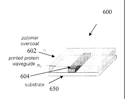
[0032] Figure 6 is a schematic illustration of a biopolymer optical
waveguide
manufactured in accordance with one embodiment of the present invention that
uses
printed proteins to form channels of the waveguide.
[0033] Figure 7 is a graph that illustrates the relationship between the
volume of
8% silk concentration vs. film thickness.
[0034] Figure 8A is a photograph of a biopolymer film made of silk.
[0035] Figure 8B is a graph showing the prism coupled angular dependence of
reflectivity of the biopolymer film of Figure 8A.
[0036] Figure 8C is a graph showing he measured transmission of light
through
the biopolymer film of Figure 8A.
-6-
CA 02704304 2014-01-24
[0037] Figure 9 illustrates results graphs showing retention of the
hemoglobin
function within an RBC-doped silk optical device.
[0038] Figure 10 is a photograph showing diffractive biopolymer devices
that
have been cast in silk, chitosan, and collagen.
[0039] Figure 11 is a histogram showing antibody IgG1 activity related to
initial
activity in the silk films prepared in the two different formats and stored at
the three
different temperatures.
[0040] Figure 12 is a histogram showing antibody IgG activity related to
initial
activity in the silk films prepared in the two different formats and stored at
the three
different temperatures.
DETAILED DESCRIPTION OF THE INVENTION
100411 As described in detail below, the biopolymer optical waveguide
devices in
accordance with the present invention have been fabricated using a biopolymer
such
as silk. In this regard, the silk utilized was silkworm silk. However, there
are many
different silks, including spider silk, transgenic silks, and genetically
engineered silks,
variants and combinations thereof and others, that may alternatively be used
in
accordance with the present invention to obtain a biopolymer optical waveguide
device.
[0042] In addition, other biodegradable polymers may be used instead of
silk. For
example, additional biopolymers, such as chitosan, exhibit desirable
mechanical
properties, can be processed in water, and form generally clear films for
optical
applications. Other biopolymers, such as chitosan, collagen, gelatin, agarose,
chitin,
polyhydroxyalkanoates, pullan, starch (amylose amylopectin), cellulose,
hyaluronic
acid, and related biopolymers, or a combination thereof, may alternatively be
utilized
in specific applications and combinations, and synthetic biodegradable
polymers such
as polylactic acid, polyglycolic acid, polyhydroxyalkanoates and related
copolymers
may also be selectively used. Some of these polymers are not as easily
processed in
water. Nonetheless, such polymers may be used by themselves, in combination
with
other polymers, or in combinations with silks, and may be used in particular
biopolymer optical devices.
-7-
CA 02704304 2014-01-24
[0043]
Figure 1 is a schematic illustration of a flow diagram 10 showing a method
of manufacturing a biopolymer optical waveguide in accordance with one
embodiment of the present invention. If a biopolymer matrix solution is
provided in
step 11, the process proceeds to step 16 below. Otherwise, a biopolymer is
provided
in step 12. In the example where the biopolymer is silk, the biopolymer may be
-7a-
CA 02704304 2014-02-13
provided by extracting sericin from the cocoons of Bombyx mori. In step 14,
the
biopolymer is processed to yield a biopolymer matrix solution.
[0042] In
step 16, the biopolymer matrix solution is processed to provide
biopolymer silk fibers, raw silk fibers or extruded fibers. In the example of
silk, an
aqueous silk fibroin solution is processed in step 16, for example, 8.0 wt %,
which is
then used to manufacture the biopolymer optical waveguide. Of course, in other
embodiments, the solution concentrations may also be varied from very dilute
(approximately 1 wt %) to very high (up to 30 wt %) using either dilution or
concentration, for example, via osmotic stress or drying techniques. In this
regard,
other embodiments may utilize different percent weight solutions to optimize
flexibility or strength of the resultant biopolymer optical waveguide,
depending on the
application. Production of aqueous silk fibroin solution is described in
detail in WIPO
Publication Number WO 2005/012606 entitled "Concentrated Aqueous Silk Fibroin
Solution and Uses Thereof'.
[0043] If
biopolymer silk fibers are provided, the silk fibers may be unwound
progressively to extract individual silk fibers in optional step 18. In
optional step 20,
the unwound biopolymer (silk) fibers are placed under tension using a
tensioning or
straightening device, such as framing elements, turnbuckles, clamp sets, and
the like.
[0044] The
fibers can also be formed synthetically as disclosed in
W004000915A2, entitled "Silk Biomaterials and Methods of Use Thereof;"
W09315244A1 entitled "Fiber-Spinnable Solutions Of Silkworm Fibroin;" and/or
U.S. Patent No. 5,252,285 entitled "Process For Making Silk Fibroin Fibers".
[0045] In
optional step 22, the silk biopolymer raw silk fibers or extruded fibers
may be treated to remove surface roughness. This optional smoothing treatment
may
be performed using low-intensity laser ablation techniques, or using other
smoothing
techniques to reduce or remove surface roughness. Additionally, the faces of
the silk
biopolymer raw or extruded fibers may be ablated to provide an improved
optical
surface for coupling light into the silk core.
[0046] In
step 24, the fibers are cast in a second polymer, such as
polydimethylsiloxane (PDMS), or the like, which acts as a polymer overcoat to
form a
- 8 -
CA 02704304 2010-04-30
WO 2008/127401
PCT/US2007/083605
biopolymer optical waveguide. Of course other materials may also be used with
which to form the over coat of the biopolymer fiber core. In step 26, the cast
fibers
and polymer overcoat are dried, and the method of manufacturing the biopolymer
optical waveguide is complete.
[0047] As illustrated schematically in Figure 2, the second material 202
forms a
polymer overcoat cladding around the biopolymer. Because the biopolymer silk
fibers
have a higher index of refraction (n=1.55) than the PDMS overcoat cladding
(n=1.46),
the combination functions as a waveguide 200 as the silk biopolymer fibers act
as a
core 204 to transmit light waves (shown as arrows 298, 299) through the second
material 202. Of course, other biopolymers such as chitosan, collagen,
gelatin,
agarose, chitin, polyhydroxyalkanoates, pullan, starch (amylose amylopectin),
cellulose, hyaluronic acid, and related biopolymers, or a combination thereof
may be
used as the core 204 as long as the second material (overcoat) 202 has a lower
index
of refraction than the selected biopolymer. In this fashion, the second
material 202,
such as the PDMS polymer overcoat, will serve as cladding material 202 to the
biopolymer core 204 of the optical waveguide 200.
[0048] Figure 2 illustrates how light waves 298, 299 are guided through the
biopolymer optical waveguide 200 of the present invention. Incident rays 299
of light
that fall within the acceptance cone 250 of the biopolymer fiber core 204 are
transmitted through the waveguide 200, whereas those incident light rays 298
that fall
outside of the acceptance cone 250 of the biopolymer fiber core204 are lost in
the
second material cladding 202.
[0049] As shown in Figure 2, the biopolymer optical waveguide 200 of the
present
invention may be manufactured in a longitudinal geometry with a circular cross-
section, where the biopolymer core 204 and the second material overcoat
cladding
202, such as PDMS, form a concentric biopolymer waveguide 200 along a
longitudinal axis, x.
[0050] Figure 3A shows a schematic illustration, and Figure 3B shows a
photograph of a biopolymer optical waveguide 300 made of silk in accordance
with
one embodiment of the present invention. As described above, the silk fiber
304 is
embedded in a polymer overcoat material 302. The index of refraction of the
silk
-9-
CA 02704304 2010-04-30
WO 2008/127401
PCT/US2007/083605
fiber 304 enables the realization of the waveguide 300 by virtue of the index
contrast
between the silk fiber 304 and the surrounding polymer overcoat material 302,
which
in the example shown in Figure 3B, is PDMS.
[0051] Of course, the biopolymer optical waveguide of the present invention
may
be manufactured with additional geometries as well. For example, the
biopolymer
optical waveguide may include a first biopolymer 404 and a polymer overcoat
402
that form a rectangular slab waveguide 400 along a planar axis (Z-axis) as
shown in
Figure 4.
[0052] Waveguides of different geometries may be formed by the method of
the
present invention including concentric waveguides with circular cross-
sectional area
as illustrated in Figure 2. Likewise, rectangular waveguides as shown in
Figure 4 may
be formed when the second polymer 402 is deposited as a guiding layer of a
slab
waveguide 400 and the biopolymer 404 is cast between layers of the slab.
Rectangular biopolymer optical waveguides manufactured in accordance with the
present invention may be used in integrated optical circuits and as a host of
optical
devices. Rectangular biopolymer optical waveguides manufactured in accordance
with the present invention may also be used as the basis of interferometers
and
wavelength division multiplexers.
[0053] The physical parameters of a rectangular waveguide help determine
the
electrical operating characteristics. The dimension of the broad wall a in
Figure 4
influences the frequency range of operation, while the dimension of the narrow
wall b
serves to establish the breakdown voltage of the wave guide and likewise the
peak
power handling capability.
[0054] In addition to uses as in vivo diagnostic light delivery components
and
therapeutic delivery components, the optical fibers of the present invention
may be
inserted in the body as transmissive media for optical radiation, and meshes
of silk
optical fibers may relay information from sensors or from different locations
within
the body.
[0055] Similarly, embedded silk fibers may serve as nondestructive
indicators of
material damage, fatigue, and failure, even when the outward appearance of the
material surface shows no damage.
-10-
CA 02704304 2010-04-30
WO 2008/127401
PCT/US2007/083605
[0056] In accordance with another embodiment of the present invention,
biopolymer optical waveguides with rectangular geometry may be produced by a
planar printing technique. This embodiment is illustrated in Figure 5, where a
method
of manufacturing a biopolymer optical waveguide 500 includes providing a
substrate
in step 502.
[0057] The substrate may be a template for an optical device, such as a
lens, a
microlens array, an optical grating, a pattern generator, a beam reshaper, and
other
optical devices. The substrate provided in step 502 serves as a mold in
manufacturing
the biopolymer optical device, which in the above example is a waveguide. A
surface
of the substrate has the desired characteristic features to be formed on the
biopolymer
optical device. In this regard, the substrate may be an appropriate
nanopattern on a
surface of the optical device and may be an optical device such as a
nanopatterned
optical grating, depending on the optical features desired for the biopolymer
optical
device being manufactured.
[0058] In step 504, a first biopolymer is printed on the substrate. The
first
biopolymer may be printed on the substrate using ink jet style printing. An
aqueous
biopolymer matrix solution may be used as the first biopolymer print medium
cast
upon the substrate by the printing process. The aqueous biopolymer matrix
solution
may then be dried in step 506 to transition the aqueous biopolymer matrix
solution to
the solid phase. In this regard, the aqueous biopolymer matrix solution may be
dried
for a period of time such as 24 hours, and may optionally be subjected to low
heat to
expedite drying of the aqueous biopolymer matrix solution. Upon drying, a
solidified
biopolymer film is formed on the surface of the substrate. The thickness of
the
biopolymer film depends on the volume of the biopolymer matrix solution
applied to
the substrate.
[0059] Once the solvent of the biopolymer matrix solution has evaporated,
the
solidified biopolymer film may optionally be annealed in step 508. This
annealing
step may be performed within a water vapor environment, such as in a chamber
filled
with water vapor, for different periods of time depending on the material
properties
desired. Typical annealing time periods may range from between two hours to
two
days, for example, and may also be performed in a vacuum environment, or in a
-11-
CA 02704304 2010-04-30
WO 2008/127401
PCT/US2007/083605
combination of environments. After an appropriate drying time, the biopolymer
film
is a suitable printed silk biopolymer layer.
[0060] In optional step 510, the printed silk biopolymer layer may be
treated to
remove surface roughness. This optional smoothing treatment may be performed
using low-intensity laser ablation techniques, or using other smoothing
techniques to
reduce or remove surface roughness. Additionally, the faces of the silk
biopolymer
layer may be ablated to provide an improved optical surface for coupling light
into the
silk core.
[0061] In step 512, a second material is deposited on the first biopolymer
to form
the biopolymer optical waveguide. The second material has a lower index of
refraction than the first biopolymer. In one embodiment, the first biopolymer
may be
silk, while in other embodiments of the present invention, a protein may be
printed on
the substrate. Similarly, in one embodiment, the second lower index of
refraction
material is polydimethylsiloxane (PDMS), while in other embodiments, other
materials may be utilized.
[0062] As illustrated above and schematically in Figure 5, the second
material
forms a polymer overcoat cladding around the biopolymer. Because the
biopolymer
silk fibers have a higher index of refraction (n=1.55) than the PDMS overcoat
cladding (n=1.46), the combination functions as a waveguide as the silk
biopolymer
fibers act as a core to transmit light through the second material. Of course,
other
biopolymers such as chitosan, collagen, gelatin, agarose, chitin,
polyhydroxyalkanoates, pullan, starch (amylose amylopectin), cellulose,
hyaluronic
acid, and related biopolymers, or a combination thereof, may be used as long
as the
second material (overcoat) has a lower index of refraction than the selected
biopolymer. In this fashion, the second material, such as the PDMS polymer
overcoat, will serve as cladding material to the biopolymer core of the
optical
waveguide.
[0063] The first biopolymer material may be deposited on the substrate in
any
efficient manner. For example, the first biopolymer material may be printed
onto the
substrate using inkjet technology, such as with an inkjet-style printer. The
first
biopolymer may be printed on the substrate by forming a layer of various
thicknesses
-12-
CA 02704304 2010-04-30
WO 2008/127401
PCT/US2007/083605
of the first biopolymer. The printing of the first biopolymer may be repeated
using
overlay printing techniques to increase the thickness of the biopolymer
waveguide,
depending upon the desired application. The (second) lower index of refraction
material is then deposited on top of the printed silk core. As mentioned
above, a
protein or other biopolymer with a higher index of refraction may also be used
as the
core material of the waveguide.
[0064] The above printing embodiment is shown schematically in Figure 6. As
shown, a substrate 650 is provided, and the protein waveguide core 604 is
printed on
the substrate 650 using inkjet technology. A lower index of refraction 602
material is
then deposited on top of the printed protein waveguide core 604. Inkjet
application
may be used to print the materials based on experimental dimensions of the
desired
printed protein waveguide. As indicated above, overlay printing of the
individual
lines of the printed protein waveguide core 604 may be necessary to build up
the
thickness of the biopolymer waveguide.
[0065] Experiments were conducted to validate the above-described method by
manufacturing various biopolymer optical waveguides. The relationship between
the
volume of 8 wt % silk concentration aqueous silk fibroin solution, and the
resulting
silk film thickness, is shown in the graph 30 of Figure 7, where the aqueous
silk
fibroin solution was cast over a substrate surface of approximately 10 square
centimeters. The X-axis shows the volume of silk fibroin solution in mL, and
the Y-
axis shows the thickness of the resultant film in m.
[0066] Of course, the film properties such as thickness and biopolymer
content, as
well as optical features, may be altered based on the concentration of fibroin
used in
the process, the volume of the aqueous silk fibroin solution deposited, and
the post-
deposition process for drying the cast solution to lock in the structure.
Accurate
control of these parameters is desirable to ensure the optical quality of the
resultant
biopolymer optical waveguide and to maintain various characteristics of the
biopolymer optical waveguide, such as transparency, structural rigidity, and
flexibility. Furthermore, additives to the biopolymer matrix solution may be
used to
alter features of the biopolymer optical waveguide such as morphology,
stability, and
the like, as known with polyethylene glycols, collagens, and the like.
-13-
CA 02704304 2010-04-30
WO 2008/127401
PCT/US2007/083605
[0067] An unpatterned biopolymer film having a thickness of 10 lam was
manufactured in the above-described manner using an aqueous silk fibroin
solution,
and was characterized in a scanning prism coupled reflectometer from Metricon
Corporation. Figure 8A illustrates the unpatterned biopolymer film 34
manufactured
and characterized. The index of refraction of the biopolymer film 34 was
measured to
be n=1.55 at 633 nm, which is slightly higher than the index of refraction of
conventional borosilicate glass. The measured index of refraction confirms
that the
value is high enough to afford reasonable contrast for optical use such as in
air-silk
biophotonic crystals (BPC) (Anfibroin Arlair = 0.55). The characterization of
the
unpatterned silk film 34 is shown in graph 36 of Figure 8B, which clearly
demonstrates the prism coupled angular dependence of the reflectivity. The
oscillations in graph 36 are due to coupling into guided waves, demonstrating
the use
of silk as a waveguide material.
[0068] In addition, the unpatterned silk film 34 was also analyzed to
determine
transparency. Figure 8C is a graph 38 that illustrates the measured
transmission of
light through the silk film 34 in various wavelengths. Transmission
measurements
indicate that the unpatterned silk film 34 was highly transparent across the
visible
spectrum. For comparison, similar thickness films were also cast in collagen,
and
polydimethylsiloxane (PDMS). The free-standing structural stability was found
to be
inferior, and the resultant biopolymer optical device was not self-supporting
when
implemented as a thin film. However, such biopolymers may be used in other
applications if structural stability is deemed to be not as important.
[0069] Importantly, shaped films having various thicknesses were patterned
on the
nanoscale using the methods of Figure 1 and Figure 5 described above to
provide
nanopatterned biopolymer optical devices.
[0070] The term "nanopatterned" as used with regard to the present
invention
refers to very small patterning that is provided on a surface of the
biopolymer optical
device. The patterning has structural features whose size can be appropriately
measured on a nanometer scale (that is, 10-9 meters), for example, sizes
ranging from
100 nm to few microns. Additionally, the biopolymer optical devices of the
present
-14-
CA 02704304 2010-04-30
WO 2008/127401
PCT/US2007/083605
invention may incorporate various different optical devices such as lenses,
diffraction
gratings, photonic crystals, waveguides, and the like.
[0071] A
variety of nanopatterned biopolymer optical devices were successfully
manufactured using the above-described method of the present invention using
silk
fibroin solution. These devices included waveguides, lenses, microlens arrays,
optical
gratings, pattern generators, and beam reshapers. In particular, the aqueous
solution
of silk fibroin was cast onto specific substrates with patterns thereon. The
substrate
surfaces were coated with TeflonTm to ensure even detachment after the
biopolymer
matrix solution transitions from the liquid to the solid phase. The ability of
the
biopolymer casting method of the present invention for forming highly defined
nanopatterned structures in biopolymer optical devices was verified by casting
the
optical waveguides of the present invention. Regular patterned features with
dimensions down to 210 nm, and localized surface roughness of less than 20 nm,
have
been attained. As mentioned above, smoothing techniques may also be used to
further
reduce or remove surface roughness of the biopolymer optical waveguide.
[0072] The
measured roughness of cast silk film on an optically flat surface
shows measured root mean squared roughness values between 2.5 and 5
nanometers,
which implies a surface roughness easily less than X/50 at a wavelength of 633
nm.
Atomic force microscope images of patterned silk diffractive optics show the
levels of
microfabrication obtainable by casting and lifting silk films off of
appropriate molds.
The images show definition in the hundreds of nanometer range and the
sharpness of
the corners indicates the possibility of faithful patterning down to the tens
of
nanometers.
[0073]
Optical losses through a silk slab waveguide obtained by guiding 633 nm
light through pure silk films of variable thickness were measured. The optical
loss
measurements varied from 0.25 to 0.75 dB/cm depending on the scattering of the
film.
With control of the purity of the silk solution and of the homogeneity of the
layers
throughout the surface losses can be further diminished to values well below
those
measured.
[0074]
Such regular patterning of biocompatible materials allows manufacturing
of optical devices that can be used to provide photonic bandgaps and
manipulate light
-15-
CA 02704304 2010-04-30
WO 2008/127401
PCT/US2007/083605
via an organic, yet mechanically robust optical device. These devices combine
the
flexibility of embedded optics with the unique versatility of the protein
substrate as
explained throughout the application. Many advantages are provided by the
present
invention including combining the organic nature of biopolymers such as silk
with the
power of diffractive and transmissive optics embedded in an organic matrix to
create
biologically active optical elements. Silk provides a controllably degradable,
biocompatible, and structurally strong medium with which to fabricate the
optical
devices in accordance with the present invention.
[0075] Transmissive nanopatterned diffractive biopolymer optical devices
were
made using the method of the present invention described above. These optical
devices include biopolymer optical waveguides, silk diffusers, line pattern
generators,
and cross pattern generators. Such optical devices use appropriately
configured
wavelength scale surface structuring to create predefined one or two-
dimensional light
patterns that exploit light interference. Such optical devices made of
conventional
materials have been applied to imaging, spectroscopy, beam sampling and
transformation, and metrology to name a few uses. Extending this approach to
control
the delivery of light within a biological matrix such as silk biopolymer can
provide
optimal coupling of photons into a substrate or allow for designed optical
discrimination, interface, or readout.
[0076] A significant advantage of biopolymer optical waveguides in
accordance
with the present invention is the ability of the optical waveguides to be
biologically
activated since they are entirely organic and biocompatible. Water-based
processing
can be used, for example, for silk optical waveguides. This increases cellular
survivability of the waveguides and the likelihood of biocompatibility.
[0077] To confirm biocompatibility of nanopatterned biopolymer optical
devices,
red blood cells (RBCs) were incorporated into a silk diffraction grating in
accordance
with the present invention that was manufactured as described above with
regard to
Figure 1 and Figure 5. The RBC-silk fibroin solution was prepared by combining
1
ml of an 80% hematocrit human RBC solution and 5 ml of the 8% silk solution.
The
mixture was cast on a 600 lines/mm optical grating and allowed to dry
overnight. The
-16-
CA 02704304 2010-04-30
WO 2008/127401
PCT/US2007/083605
film was removed from the optical grating and annealed for two hours. The
grating
structure was observed in the resultant RBC-doped silk diffraction grating.
[0078] The RBC-doped silk diffraction grating was then tested to observe
the
diffraction orders. An optical transmission experiment was performed to
determine
whether hemoglobin (the oxygen-carrying protein contained in RB Cs) maintained
its
activity within the matrix of the silk diffraction grating. The results graphs
160 are
shown in Figure 9 and indicate the retention of hemoglobin function within the
RBC-
doped silk diffraction grating. The X-axis corresponds to the wavelength (in
nm), and
the Y-axis indicates the absorbance by the RBC-doped silk diffraction grating.
[0079] In particular, the RBC-doped silk diffraction grating was inserted
in a
quartz cuvette filled with distilled water, and an absorbance curve was
observed. This
result is shown by line (b) Hb02 in results graphs 160. As can be seen, the
absorbance
curve shown by line (b) Hb02 exhibited two peaks typical of oxy-hemoglobin
absorption. Subsequently, nitrogen gas was bubbled into the cuvette to
deoxygenate
the hemoglobin. After 15 minutes, the characteristic absorption peaks of oxy-
hemoglobin disappeared from the absorbance curve. This result is shown by line
(a)
Hb in the results graphs 160. These results were further confirmed when the
nitrogen
flow to the cuvette is subsequently halted, which resulted in the reappearance
of the
oxy-hemoglobin peaks. This result is shown by line (c) Hb02 in results graphs
160.
[0080] As previously noted, alternative biopolymers may also be used for
fabrication of nanopatterned biopolymer optical devices in accordance with the
present invention. Figure 10 shows a photograph 180 that illustrates other
diffractive
biopolymer optical devices that have been cast using different materials. In
particular,
a chitosan optical device 182 and a collagen optical device 184 have also been
manufactured in accordance with the present invention. With respect to
chitosan,
optical diffraction characteristics similar to silk have been observed.
[0081] It should be evident from the above discussion and the example
nanopatterned biopolymer optical devices shown and discussed that the present
invention provides biodegradable nanopatterned biopolymer optical devices.
High
quality nanopatterned biopolymer optical devices were manufactured that are
naturally biocompatible, can be processed in water, and can undergo
degradation with
-17-
CA 02704304 2010-04-30
WO 2008/127401
PCT/US2007/083605
controlled lifetimes. As explained above, the nanopatterned biopolymer optical
devices of the present invention may also be biologically activated by
incorporating
small organic materials. For example, the small organic materials may be
complex
proteins such as hemoglobin in the red blood cells and enzymes such as
peroxidase.
The present invention broadens the versatility of optical devices by allowing
the direct
incorporation of labile biological receptors in the form of peptides, enzymes,
cells,
antibodies, or related systems, and allows such optical devices to function as
biological sensing devices. Thus, the organic material can be a nucleic acid,
a dye, a
cell, an antibody, as described further in Appendix I, enzymes, for example,
peroxidase, lipase, amylose, organophosphate dehydrogenase, ligases,
restriction
endonucleases, ribonucleases, DNA polymerases, glucose oxidase, laccase,
cells,
viruses, bacterias, proteins, peptides for molecular recognition, small
molecules,
drugs, dyes, amino acids, vitamins, antixoxidants, plant cells, mammalian
cells, and
the like, DNA, RNA, RNAi, lipids, nucleotides, aptamers, carbohydrates,
optically-
active chromophores ncluding beta carotene or porphyrinsõ light emitting
organic
compounds such as luciferin, carotenes and light emitting inorganic compounds,
chemical dyes, antibiotics, yeast, antifungals, antivirals, and complexes such
as
hemoglobin, electron transport chain coenzymes and redox components,light
harvesting compounds such as chlorophyll, phycobiliproteins,
bacteriorhodopsin,
protorhodopsin, and porphyrins and related electronically active compounds, or
a
combination thereof.
[0082] The nanopatterned biopolymer optical devices of the present
invention can
be readily used in environmental and life sciences where biocompatibility and
biodegradability are paramount. For example, the nanopatterned biopolymer
optical
devices as described above can be unobtrusively used to monitor a natural
environment such as in the human body and may be implanted in vivo without a
need
to retrieve the device at a later time. The degradation lifetime of the
nanopatterned
biopolymer optical devices of the present invention can be controlled during
the
manufacturing process, for example, by controlling the ratio and amount of the
solution matrix cast. Moreover, the nanopatterned biopolymer optical devices
of the
present invention can be dispersed in the environment, again without the need
to
-18-
CA 02704304 2010-04-30
WO 2008/127401
PCT/US2007/083605
retrieve them at a later time, thereby providing novel and useful devices for
sensing
and detection.
[0083] The foregoing description of the aspects and embodiments of the
present
invention provides illustration and description, but is not intended to be
exhaustive or
to limit the invention to the precise form disclosed. Those of skill in the
art will
recognize certain modifications, permutations, additions, and combinations of
those
embodiments are possible in light of the above teachings or may be acquired
from
practice of the invention. Therefore the present invention also covers various
modifications and equivalent arrangements that fall within the purview of the
appended claims.
-19-
CA 02704304 2010-04-30
WO 2008/127401 PCT/US2007/083605
APPENDIX I
Antibody Stability in Silk Films
Materials - Anti-IL-8 monoclonal antibody (IgG1) was purchased from
eBioscience. Inc. human
polyclonal antibody IgG and human IgG ELISA Quantitation Kit were purchased
from Bethyl
Laboratories Inc. All other chemicals used in the study were purchased from
Sigma-Aldrich (St.
Louis, MO).
Antibody entrapment in silk films - human polyclonal antibody IgG ¨ Ten ml
lmg/m1 IgG
mixed with 167 ml 6% silk solution make the IgG concentration in silk film
mg/g silk. 100 Ill
of mixed IgG solution was added to each well of 96 well plate which was placed
in a fume
hood with cover opened overnight. The dried film was either treated or not
treated with
methanol. For methanol treatment, the wells were immersed in 90% methanol
solution for 5
min and dried in the fume hood. All dry 96 well plates were then stored at 4
C, room
temperature, and 37 C.
Anti-IL-8 monoclonal antibody (IgG1) - 0.5ml 1 mg/ml IgG1 mixed with 83 ml 6%
silk
solution make the IgG1 concentration in silk film 0.1 mg/g silk. 50 ii.t1 of
mixed IgG1 solution
was added to a well of 96 well plate which was placed in a fume hood with
cover opened
overnight. The dried film was either treated or not treated with methanol. For
methanol
treatment, the wells were immersed in 90% methanol solution for 5 min and
dried in the
fume hood. All dry 96 well plates were then stored at 4 C, room temperature,
and 37 C.
Antibody measurement - Five wells prepared at the same condition were measured
for
statistic. Pure silk (without antibody) was used as a control.
For non methanol-treated samples, 100 ial of PBS buffer, pH 7.4, was added to
the well
which was further incubated at room temperature for 30 min to allow the film
to completely
dissolve. Aliquot of solution was then subjected to antibody measurement. For
methanol-
treated samples, 100 ial HFIP was added into each well which was further
incubated at room
temperature for 2 hours to allow the film completely dissolve. The silk HFIP
solution was
dried in a fume hood overnight. The follow step was the same as non methanol-
treated
samples, added PBS buffer and pipette the solution for antibody measurement.
ELISA - Polystyrene (96-well) microtitre plate was coated with 100 ittL of
antigen anti-
Human IgG-affinity at a concentration of 10 Kg/mL prepared in antigen coating
buffer
(bicarbonate buffer, 50 mM, pH 9.6) and then incubated overnight storage at
room
temperature. The wells were then washed three times with TBS-T buffer. The
unoccupied
sites were blocked with 1% BSA in TBS (200 ittL each well) followed by
incubation for 30
minutes at room temperature. The wells were then washed three times with TBS-
T. The test
and control wells were then diluted with 100 ittL of serially diluted serum.
Each dilution was
in TBS buffer. Serially diluted blanks corresponding to each dilution were
also present. The
plate was then incubated for 1 h at room temperature. The plate was washed
again with TBS-
T buffer (five times). Bound antibodies were assayed with an appropriate
conjugate of anti-
human IgG-HRP (1:100,000), 100 ittL of it was coated in each well and kept at
room
-20-
CA 02704304 2014-01-24
temperature for 1 hour. Washing of the plate with TBS-T (five times) was
followed by addition of 100 fit TMB in each well and incubation at room
temperature for 5-20 min. The absorbance of each well was monitored at 450 nm
on a VersaMaxTm microplate reader (Molecular devices, Sunnyvale, CA). Results
are
illustrated in Figures 11 and 12.
-21-