Note: Descriptions are shown in the official language in which they were submitted.
CA 02704769 2013-07-04
NANOPATTERNED BIOPOLYMER OPTICAL DEVICE AND
METHOD OF MANUFACTURING THE SAME
BACKGROUND OF THE INVENTION
Field of the Invention
[0003] The present invention is directed to nanopatterned biopolymer
optical
devices, and methods for manufacturing such devices.
Description of Related Art
[0004] The field of optics is well established. Some subfields of optics
include
diffractive optics, micro-optics, photonics and guided wave optics. Various
optical
devices have been fabricated in these and other subfields of optics for
research and
commercial application. For example, common optical devices include
diffraction
gratings, photonic crystals, optofluidic devices, waveguides, and the like.
[0005] These optical devices are fabricated using various methods depending
on
the application and optical characteristics desired. However, these optical
devices,
and the fabrication methods employed in their manufacture, generally involve
significant use of non-biodegradable materials. For example, glass, fused
silica, and
-1-
CA 02704769 2010-04-30
WO 2008/127404 PCT/US2007/083642
plastic are commonly used in optical devices. Such materials are not
biodegradable
and remain in the environment for extended periods of time after the optical
devices
are removed from service and discarded. Of course, some of the materials can
be
recycled and reused. However, recycling also requires expenditures of natural
resources, and adds to the environmental costs associated with such materials.
[0006] Therefore, there exists an unfulfilled need for optical devices that
minimize
the negative impact to the environment. In addition, there exists an
unfulfilled need
for optical devices that provide additional functional features that are not
provided by
conventional optical devices.
SUMMARY OF THE INVENTION
[0007] In view of the foregoing, objects of the present invention are to
provide
various novel biopolymer optical devices and methods for manufacturing such
optical
devices that may be used in various applications.
[0008] One aspect of the present invention is to provide nanopatterned
biopolymer
optical devices.
[0009] Another aspect of the present invention is to provide a method for
manufacturing such nanopatterned biopolymer optical devices.
[0010] One advantage of the present invention is in providing optical
devices that
minimize the negative impact to the environment.
[0011] Another advantage of the present invention is in providing optical
devices
that are biocompatible.
[0012] Yet another advantage of the present invention is in providing
optical
devices that have additional functional features that are not provided by
conventional
optical devices.
[0013] In the above regard, inventors of the present invention recognized
that
biopolymers, and especially silk proteins, present novel structure and
resulting
functions. For example, from a materials science perspective, silks spun by
spiders
and silkworms represent the strongest and toughest natural fibers known and
present
various opportunities for functionalization, processing, and biocompatibility.
Over
five millennia of history accompany the journey of silk from a sought-after
textile to a
-2-
CA 02704769 2010-04-30
WO 2008/127404 PCT/US2007/083642
scientifically attractive fiber. As much as its features had captivated people
in the
past, silk commands considerable attention in this day and age because of its
strength,
elasticity, and biochemical properties. The novel material features of silks
have
recently been extended due to insights into self-assembly and the role of
water in
assembly. These insights, in turn, have led to new processing methods to
generate
hydrogels, ultrathin films, thick films, conformal coatings, three-dimensional
porous
matrices, solid blocks, nanoscale diameter fibers, and large diameter fibers.
[0014] Silk-based materials achieve their impressive mechanical properties
with
natural physical crosslinks of thermodynamically stable protein secondary
structures
also known as beta sheets (I3-sheets). Thus, no exogenous crosslinking
reactions or
post-processing crosslinking is required to stabilize the materials. The
presence of
diverse amino acid side chain chemistries on silk protein chains facilitates
coupling
chemistry to functionalize silks, such as with cytokines, morphogens, and cell
binding
domains. There are no known synthetic or biologically-derived polymer systems
that
offer this range of material properties or biological interfaces, when
considering
mechanical profiles, aqueous processing, ease of functionalization, diverse
modes of
processing, self-forming crosslinks, biocompatibility, and biodegradability.
[0015] While no other biopolymer or synthetic polymer can match the range
of
features outlined above for silk, the inventors of the present invention have
identified
some other polymers that exhibit various properties similar or analogous to
silk. In
particular, other natural biopolymers including chitosan, collagen, gelatin,
agarose,
chitin, polyhydroxyalkanoates, pullan, starch (amylose amylopectin),
cellulose,
hyaluronic acid, and related biopolymers, or a combination thereof, have been
identified. In view of the above noted features of biopolymers and of silk in
particular, the present invention provides various novel nanopatterned
biopolymer
optical devices and methods for manufacturing such devices.
[0016] In accordance with one aspect of the present invention, one method
of
manufacturing a nanopatterned biopolymer optical device includes providing a
biopolymer, processing the biopolymer to yield a biopolymer matrix solution,
providing a substrate with a nanopatterned surface, casting the biopolymer
matrix
solution on the nanopatterned surface of the substrate, and drying the
biopolymer
-3-
CA 02704769 2010-04-30
WO 2008/127404 PCT/US2007/083642
matrix solution to form a solidified biopolymer film on the substrate. The
solidified
biopolymer film includes a nanopattern on its surface. In another embodiment,
the
method also includes optionally annealing the solidified biopolymer film and
further
drying the annealed biopolymer film. In this regard, the optional annealing of
the
solidified biopolymer film may be performed in a vacuum environment, in a
water
vapor environment, or in a combination of both environments.
[0017] In
accordance with various embodiments of the present invention, the
substrate and the manufactured biopolymer optical device may be a lens, a
microlens
array, an optical grating, a pattern generator, or a beam reshaper. In one
embodiment,
the biopolymer is silk, and the biopolymer matrix solution is an aqueous silk
fibroin
solution having approximately 1.0 wt % to 30 wt % silk, inclusive, such as an
aqueous
silk fibroin solution having approximately 8.0 wt% silk. Of
course, other
embodiments may utilize different percent weight solutions to optimize
flexibility or
strength of the resultant nanopatterned biopolymer optical device, depending
on the
application, while maintaining the desired optical functions. In other
embodiments,
the biopolymer may be chitosan, collagen, gelatin, agarose, chitin,
polyhydroxyalkanoates, pullan, starch (amylose amylopectin), cellulose,
hyaluronic
acid, and related biopolymers, or a combination thereof.
[0018] In
accordance with another embodiment, the method of manufacturing a
nanopatterned biopolymer optical device further includes embedding an organic
material in the solidified biopolymer film, and/or adding an organic material
into the
biopolymer matrix solution. The organic material may be red blood cells,
horseradish
peroxidase, or phenolsulfonphthalein, or a combination of these organic
materials.
The organic material may also be a nucleic acid, a dye, a cell, an antibody,
enzymes,
for example, peroxidase, lipase, amylose, organophosphate dehydrogenase,
ligases,
restriction endonucleases, ribonucleases, DNA polymerases, glucose oxidase,
laccase,
cells, viruses, proteins, peptides, small molecules, drugs, dyes, amino acids,
vitamins,
antixoxidants, DNA, RNA, RNAi, lipids, nucleotides, aptamers, carbohydrates,
chromophores, light emitting organic compounds such as luciferin, carotenes
and light
emitting inorganic compounds, chemical dyes, antibiotics, antifungals,
antivirals, light
-4-
CA 02704769 2010-04-30
WO 2008/127404 PCT/US2007/083642
harvesting compounds such as chlorophyll, bacteriorhodopsin, protorhodopsin,
and
porphyrins and related electronically active compounds, or a combination
thereof.
[0019] Other materials may be embedded in the biopolymer or in the
biopolymer
matrix solution instead of, or in addition to, organic materials, depending
upon the
type of optical device desired.
[0020] In accordance with another aspect of the present invention, a
nanopatterned
biopolymer optical device is provided that includes a solidified biopolymer
film with a
surface having a nanopattern thereon. In various embodiments, the biopolymer
optical device may be an optical grating, a lens, a microlens array, a pattern
generator,
or a beam reshaper.
[0021] These and other advantages and features of the present invention
will
become more apparent from the following detailed description of the preferred
embodiments of the present invention when viewed in conjunction with the
accompanying drawings.
BRIEF DESCRIPTION OF THE DRAWINGS
[0022] Figure 1 is a schematic flow diagram illustrating a method in
accordance
with one embodiment of the present invention.
[0023] Figure 2 is a graph that illustrates the relationship between the
volume of
8% silk concentration vs. film thickness.
[0024] Figure 3A is a photograph of an unpatterned silk film.
[0025] Figure 3B is a graph showing the prism coupled angular dependence of
reflectivity of the unpatterned silk film of Figure 3A.
[0026] Figure 3C is a graph showing the measured transmission of light
through
the silk film of Figure 3A.
[0027] Figure 4A is a photograph of a nanopatterned biopolymer focusing
lens in
accordance with one embodiment of the present invention.
[0028] Figure 4B is a microscope image of the nanopatterned biopolymer
focusing
lens of Figure 4A.
[0029] Figure 5 is a photograph of image of lettering viewed through the
nanopatterned biopolymer focusing lens of Figure 4A.
-5-
CA 02704769 2010-04-30
WO 2008/127404 PCT/US2007/083642
[0030] Figure 6A is a photograph of a nanopatterned biopolymer lens array
in
accordance with another embodiment of the present invention.
[0031] Figure 6B is a photograph of lettering as viewed through the
nanopatterned
biopolymer lens array of Figure 6A.
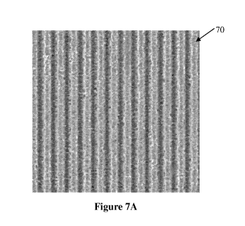
[0032] Figure 7A is a scanning electron microscope image of a portion of a
nanopatterned biopolymer diffraction grating in accordance with another
embodiment
of the present invention.
[0033] Figure 7B is an atomic force microscope image of another portion of
the
nanopatterned biopolymer diffraction grating of Figure 7A.
[0034] Figure 7C is a high-resolution atomic force microscope image of
another
portion of the nanopatterned biopolymer diffraction grating of Figure 7A.
[0035] Figure 8 is a high-resolution atomic force microscope image of a
portion of
another nanopatterned biopolymer diffraction grating in accordance with
another
embodiment of the present invention.
[0036] Figure 9A is a photograph showing the diffracted orders from a
supercontinuum laser source impinging on a nanopatterned biopolymer
diffraction
grating in accordance with the present invention.
[0037] Figure 9B is a photograph showing the diffracted orders from a
supercontinuum laser source impinging on another nanopatterned biopolymer
diffraction grating in accordance with the present invention.
[0038] Figure 10A is a photograph showing a broad white light laser
transmitted
through another nanopatterned biopolymer diffractive grating in accordance
with the
present invention.
[0039] Figure 10B is a photograph showing a broad white light laser
transmitted
through yet another nanopatterned biopolymer diffractive element in accordance
with
the present invention.
[0040] Figures 11A through 11C show far field images photographed after
transmitting broadband white light laser through nanopatterned biopolymer
optical
devices in accordance with the present invention.
[0041] Figure 12A shows a scanning electron microscope image of a surface
of a
nanopatterned biopolymer diffraction grating before surface processing.
-6-
CA 02704769 2013-07-04
[0042] Figure 12B shows a scanning electron microscope image of the surface
of
the nanopatterned biopolymer diffraction grating of Figure 12A after surface
processing.
[0043] Figures 12C and 12D show schematic illustrations of the surface of
the
nanopatterned biopolymer diffraction grating shown in Figures 12A and 12B,
respectively.
[0044] Figure 13 shows a schematic illustration of immersion of a silk
fibroin
diffraction grating in corneal fibroblast, and photographs illustrating its
impact on
diffraction.
[0045] Figure 14A shows the resultant efficient diffraction as a laser beam
is
propagated through a nanopatterned silk diffraction grating in a buffer
solution.
[0046] Figure 14B shows the comparative loss of diffraction properties with
the
silk diffraction grating in a corneal fibroblast solution.
[0047] Figure 15A is a photograph of a spectral image generated when
supercontinuum light is transmitted through an undoped nanopatterned silk
diffraction
grating in accordance with the present invention.
[0048] Figure 15B is a photograph of a spectral image generated when
supercontinuum light is transmitted through another nanopatterned silk
diffraction
grating embedded with phenolsulfonphthalein in accordance with the present
invention.
[0049] Figure 15C is a photograph of a spectral image generated when
supercontinuum light is transmitted through the nanopatterned silk diffraction
grating
of Figure 15B when it is exposed to a base solution.
[0050] Figure 16 is a results graph showing spectral absorbance of a red
blood cell
doped silk diffraction grating.
[0051] Figure 17 is a results graph showing spectral absorbance of a
horseradish
peroxidase embedded silk diffraction grating.
[0052] Figure 18 illustrates diffractive biopolymer optical devices that
have been
cast with chitosan and collagen.
[0053] Figure 19 illustrates antibody IgG1 activity related to initial in
the silk
films prepared in the two different formats and stored at the three different
temperatures.
[0054] Figure 20 illustrates antibody IgG activity related to initial
activity in the
silk films prepared in the two different formats and stored at the three
different
temperatures.
-7-
CA 02704769 2010-04-30
WO 2008/127404 PCT/US2007/083642
DETAILED DESCRIPTION OF THE INVENTION
[0053] As described in detail below, the nanopatterned biopolymer optical
devices
in accordance with the present invention have been fabricated using a
biopolymer
such as silk. In this regard, the silk utilized was silkworm silk. However,
there are
many different silks, including spider silk, transgenic silks, and genetically
engineered
silks, variants and combinations thereof and others, that may alternatively be
used in
accordance with the present invention to obtain a nanopatterned biopolymer
optical
device.
[0054] In addition, other biodegradable polymers may be used instead of
silk. For
example, additional biopolymers, such as chitosan, exhibit desirable
mechanical
properties, can be processed in water, and form generally clear films for
optical
applications. Other biopolymers, such as chitosan, collagen, gelatin, agarose,
chitin,
polyhydroxyalkanoates, pullan, starch (amylose amylopectin), cellulose,
hyaluronic
acid, and related biopolymers, or a combination thereof, may alternatively be
utilized
in specific applications, and synthetic biodegradable polymers such as
polylactic acid,
polyglycolic acid, polyhydroxyalkanoates and related copolymers may also be
selectively used. Some of these polymers are not as easily processable in
water.
Nonetheless, such polymers may be used by themselves, or in combinations with
silks, and may be used in particular biopolymer optical devices.
[0055] The term "nanopatterned" as used with regard to the present
invention
refers to very small patterning that is provided on a surface of the
biopolymer optical
device. The patterning has structural features whose size can be appropriately
measured on a nanometer scale (that is, 10-9 meters), for example, sizes
ranging from
100 nm to few microns. Additionally, the biopolymer optical devices of the
present
invention may incorporate various different optical devices such as lenses,
diffraction
gratings, photonic crystals, waveguides, and the like.
[0056] Figure 1 is a schematic illustration of a flow diagram 10 showing a
method
of manufacturing a nanopatterned biopolymer optical device in accordance with
one
embodiment of the present invention. If a biopolymer matrix solution is
provided in
step 11, the process proceeds to step 16 described below. Otherwise, a
biopolymer is
provided in step 12. In the example where the biopolymer is silk, the
biopolymer may
-8-
CA 02704769 2010-04-30
WO 2008/127404 PCT/US2007/083642
be attained by extracting sericin from the cocoons of Bombyx mori. The
provided
biopolymer is processed to yield a biopolymer matrix solution in step 14. In
one
embodiment, the biopolymer matrix solution is an aqueous matrix solution.
However,
in other embodiments, different solvents other than water, or a combination of
water
and other solvents may be used, depending on the biopolymer used.
[0057] Thus, in the example of silk, an aqueous silk fibroin solution is
processed
in step 14, for example, 8.0 wt %, which is then used to manufacture the
nanopatterned biopolymer optical device. Of course, in other embodiments, the
solution concentrations may also be varied from very dilute (approximately 1
wt %) to
very high (up to 30 wt %) using either dilution or concentration, for example,
via
osmotic stress or drying techniques. In this regard, other embodiments may
utilize
different percent weight solutions to optimize flexibility or strength of the
resultant
nanopatterned biopolymer optical device, depending on the application.
Production of
aqueous silk fibroin solution is described in detail in WIPO Publication
Number WO
2005/012606 entitled "Concentrated Aqueous Silk Fibroin Solution and Uses
Thereof".
[0058] A substrate is provided in step 16 to serve as a mold in
manufacturing the
biopolymer optical device. A surface of the substrate has the desired
characteristic
features to be formed on the biopolymer optical device. In this regard, the
substrate
may be an appropriate nanopattern on a surface of the optical device and may
be an
optical device such as a nanopatterned optical grating, depending on the
optical
features desired for the biopolymer optical device being manufactured. The
aqueous
biopolymer matrix solution is then cast on the substrate in step 18. The
aqueous
biopolymer matrix solution is then dried in step 20 to transition the aqueous
biopolymer matrix solution to the solid phase. In this regard, the aqueous
biopolymer
matrix solution may be dried for a period of time such as 24 hours, and may
optionally
be subjected to low heat to expedite drying of the aqueous biopolymer matrix
solution.
Upon drying, a solidified biopolymer film is formed on the surface of the
substrate.
The thickness of the biopolymer film depends on the volume of the biopolymer
matrix
solution applied to the substrate.
-9-
CA 02704769 2010-04-30
WO 2008/127404 PCT/US2007/083642
[0059] Once the solvent of the biopolymer matrix solution has evaporated,
the
solidified biopolymer film may be optionally annealed in step 22. This
annealing step
is preferably performed within a water vapor environment, such as in a chamber
filled
with water vapor, for different periods of time depending on the material
properties
desired. Typical annealing time periods may range from between two hours to
two
days, for example, and may also be performed in a vacuum environment. The
annealed biopolymer film is then removed from the substrate in step 24 and
allowed to
dry further in step 26, thereby resulting in a biopolymer optical device. The
annealed
films manufactured in the above-described manner have a functional optical
surface
that matches the surface provided on the substrate. The annealed film can then
be
used as a nanopatterned biopolymer optical device in accordance with the
present
invention.
[0060] Experiments were conducted to validate the above-described method by
manufacturing various biopolymer optical devices. The relationship between the
volume of 8 wt % silk concentration aqueous silk fibroin solution, and the
resulting
silk film thickness, is shown in the graph 30 of Figure 2, where the aqueous
silk
fibroin solution was cast over a substrate surface of approximately 10 square
centimeters. The X-axis shows the volume of silk fibroin solution in mL, and
the Y-
axis shows the thickness of the resultant film in pm.
[0061] Of course, the film properties such as thickness and biopolymer
content, as
well as optical features, may be altered based on the concentration of fibroin
used in
the process, the volume of the aqueous silk fibroin solution deposited, and
the post
deposition process for drying the cast solution to lock in the structure.
Accurate
control of these parameters is desirable to ensure the optical quality of the
resultant
biopolymer optical device and to maintain various characteristics of the
biopolymer
optical device, such as transparency, structural rigidity, and flexibility.
Furthermore,
additives to the biopolymer matrix solution may be used to alter features of
the
biopolymer optical device such as morphology, stability, and the like, as
known with
polyethylene glycols, collagens, and the like.
[0062] An unpatterned biopolymer film having a thickness of 101tm was
manufactured in the above-described manner using an aqueous silk fibroin
solution,
-10-
CA 02704769 2010-04-30
WO 2008/127404 PCT/US2007/083642
and was characterized in a scanning prism coupled reflectometer from Metricon
Corporation. Figure 3A illustrates the unpatterned biopolymer film 34
manufactured
and characterized. The index of refraction of the biopolymer film 34 was
measured to
be n=1.55 at 633 nm, which is slightly higher than the index of refraction of
conventional borosilicate glass. The measured index of refraction confirms
that the
value is high enough to afford reasonable contrast for optical use such as in
air-silk
biophotonic crystals (BPC) (Anfibroin Arlair = 0.55). The characterization of
the
unpatterned silk film 34 is shown in graph 36 of Figure 3B, which clearly
demonstrates the prism coupled angular dependence of the reflectivity. The
oscillations in graph 36 are due to coupling into guided waves, demonstrating
the use
of silk as a waveguide material.
[0063] In addition, the unpatterned silk film 34 was also analyzed to
determine
transparency. Figure 3C is a graph 38 that illustrates the measured
transmission of
light through the silk film 34 in various wavelengths. Transmission
measurements
indicate that the unpatterned silk film 34 was highly transparent across the
visible
spectrum. For comparison, similar thickness films were also cast in collagen,
and
polydimethylsiloxane (PDMS). The free-standing structural stability was found
to be
inferior, and the resultant biopolymer optical device was not self-supporting
when
implemented as a thin film. However, such biopolymers may be used in an
application if structural stability is deemed to be not as important.
[0064] Importantly, shaped films having various thicknesses were patterned
on the
nanoscale using the method of Figure 1 described above to provide
nanopatterned
biopolymer optical devices. A variety of nanopatterned biopolymer optical
devices
were successfully manufactured using the above-described method of the present
invention using silk fibroin solution. These devices included lenses,
microlens arrays,
optical gratings, pattern generators and beam reshapers. In particular, the
aqueous
solution of silk fibroin was cast onto specific substrates with patterns
thereon. The
substrate surfaces were coated with TeflonTm to ensure even detachment after
the
biopolymer matrix solution transitions from the liquid to the solid phase. The
ability
of the biopolymer casting method of the present invention for forming highly
defined
nanopatterned structures in biopolymer optical devices was verified by casting
-11-
CA 02704769 2010-04-30
WO 2008/127404 PCT/US2007/083642
diffraction gratings and lenses. Regular patterned features with dimensions
down to
210 nm, and localized surface roughness of less than 20 nm, have been
attained.
[0065] Such regular patterning of biocompatible materials allows
manufacturing
of optical devices that can be used to provide photonic bandgaps and
manipulate light
via an organic, yet mechanically robust optical device. These devices combine
the
flexibility of embedded optics with the unique versatility of the protein
substrate as
explained in further detail below. Many advantages are provided by the present
invention including combining the organic nature of biopolymers such as silk
with the
power of diffractive and transmissive optics embedded in an organic matrix to
create
biologically active optical elements. Silk provides a controllably degradable,
biocompatible, and structurally strong medium with which to fabricate the
optical
devices in accordance with the present invention.
[0066] Figure 4A is a photograph showing a nanopatterned biopolymer
focusing
lens 40 that was manufactured using the method described above with an aqueous
silk
fibroin solution. The biopolymer focusing lens 40 has a diameter of less than
1
centimeter and has nanopatterned concentric rings formed on its surface.
Figure 4B is
a microscopic image 42 of the biopolymer focusing lens 40 shown in Figure 4A.
The
microscopic image 42 clearly shows the nanopatterned concentric rings 44 on
the
biopolymer focusing lens.
[0067] Figure 5 shows a photograph image 50 of lettering "Tufts" as seen
through
the nanopatterned focusing lens 40 of Figure 4A. This photograph clearly
illustrates
the optical applicability of optical devices made of biopolymers that are
manufactured
in accordance with the method of the present invention.
[0068] In addition, nanopatterned biopolymer optical devices were
manufactured
by casting the aqueous silk fibroin solutions on microlens arrays and on other
pattern
generators. In particular, the aqueous silk fibroin solution was cast on
various
patterned surfaces of optical elements, left to solidify, and subsequently
annealed in
accordance with the method described above with regard to Figure 1. Figures 6A
and
6B are photographs of a lens array 60 manufactured in accordance with the
present
invention using aqueous silk fibroin solution. The lens array 60 was cast on a
polycarbonate film from Digital Optics Corporation. The obtained silk lens
array 60
-12-
CA 02704769 2010-04-30
WO 2008/127404 PCT/US2007/083642
is approximately 1 cm2 in size and is patterned with 12x12 lenses 62 thereon.
The
lenses 62 provided on the lens array 60 demonstrate that accurately patterned
biopolymer optical devices can be manufactured by casting a biopolymer matrix
solution, such as an aqueous silk fibroin solution, on a substrate that
functions as a
mold. Figure 6B is a photograph of text as seen through the silk lens array
60.
[0069] In addition, holographic diffraction gratings of various line
pitches were
also used as substrates upon which an aqueous silk fibroin solution was cast
for
manufacturing nanopatterned biopolymer diffraction gratings in accordance with
the
present invention. In this regard, Figure 7A is a scanning electron microscope
image
of a portion of a nanopatterned biopolymer diffraction grating 70 that was
manufactured in accordance with the method of Figure 1 by casting an aqueous
silk
fibroin solution on a holographic diffraction grating with 2,400 lines/mm. The
resultant biopolymer diffraction grating 70 of silk also has gratings 72 at
2,400
lines/mm. Figures 7B and 7C are atomic force microscope (AFM), and high-
resolution AFM images, respectively, of a portion of the surface of the
nanopatterned
biopolymer diffraction grating 70. The portion of the diffraction grating 70
shown in
Figure 7C is approximately 1 tm2. As shown, the ridges of the grating were
approximately 200nm wide and spaced by approximately 200 nm at full width at
half
maximum (FWHM). The peak to valley height difference of 150 nm was observed.
[0070] As can be seen from the AFM images of Figures 7B and 7C,
nanopatterned
biopolymer diffraction grating 70 had highly regular, structured gratings 72
on the
nanoscale with remarkably smooth sidewalls 74. A topographical evaluation of
the
surface roughness at the peaks of the gratings 72 and valleys between the
gratings 72
revealed surface roughness root mean square (RMS) values below 20 nm while
being
structurally stable. These values characterize outstanding resolution from
optics and
materials perspectives.
[0071] The measured roughness of cast silk film on an optically flat
surface
shows measured root mean squared roughness values between 2.5 and 5
nanometers,
which implies a surface roughness easily less than X/50 at a wavelength of 633
nm.
Atomic force microscope images of patterned silk diffractive optics show the
levels of
microfabrication obtainable by casting and lifting silk films off of
appropriate molds.
-13-
CA 02704769 2010-04-30
WO 2008/127404 PCT/US2007/083642
The images show definition in the hundreds of nanometer range and the
sharpness of
the corners indicates the possibility of faithful patterning down to the tens
of
nanometers.
[0072] Figure 8 is a high-resolution atomic force microscope (AFM) image of
a
1[tm2 portion of a nanopatterned silk diffraction grating 80 that was also
manufactured
in accordance with the method of the present invention by casting aqueous silk
fibroin
solution on an optical diffraction grating having a pitch of 3,600 lines/mm.
The
resultant biopolymer diffraction grating 80 also has 3,600 lines/mm. The
structured
gratings 82 were measured to be 125 nm apart at FWHM with a peak to valley
height
difference of 60 nm. As can be seen, highly regular structured gratings 82 on
the
nanoscale were obtained with remarkably smooth sidewalls. Topographic analysis
of
the surfaces again revealed a surface roughness of less than 20 nanometers
RMS.
[0073] Other example diffraction gratings of different line pitches, and
different
sizes as large as 50 x 50 mm, were also manufactured using the method of the
present
invention. In this regard, diffraction gratings having 600 lines/mm and 1,200
lines/mm were also used to manufacture nanopatterned biopolymer diffraction
gratings. The resultant nanopatterned biopolymer diffraction gratings were
found to
reproduce the fine features with a surface smoothness having RMS less than 20
nm
while being structurally stable. In certain areas, the smoothness was found to
have
RMS roughness of less than 10 nm.
[0074] Samples of patterned biopolymer diffraction gratings were optically
analyzed by transmitting both single wavelength and white (supercontinuum)
coherent
light through the silk diffraction gratings to examine the diffraction
properties. Figure
9A is a photograph 90 that illustrates diffracted orders from a white light
laser source
impinging on a silk diffraction grating manufactured in accordance with the
present
invention. As can be seen, central order and three diffraction orders were
observed.
The measured diffraction efficiency in the m = 1 and m = -1 orders was
approximately
37% in the illustrated experiment. Radiation with an average power approaching
1 W
was transmitted through the silk diffraction grating successfully without
damaging the
diffraction grating structure.
-14-
CA 02704769 2010-04-30
WO 2008/127404 PCT/US2007/083642
[0075] Figure 9B is another photograph 96 that illustrates diffracted
orders from a
supercontinuum laser source impinging on a silk diffraction grating with 1,200
lines/mm that was made in accordance with the present invention. The
diffracted
orders were imaged 2 cm from the silk diffraction grating. The diffraction
efficiency
of this grating was found to be 34% in the first order at 633 nm, which
compares
favorably to conventional transmissive glass gratings.
[0076] The structural stability and the ability to faithfully reproduce
nanostructures makes the above-described method an excellent process for
manufacturing many different diffractive optical structures or refractive
micro and
nano-optical structures. Among the various optical devices that can be readily
manufactured are optical gratings, micro and nano lens arrays as described
above,
pattern generators, beam diffusers, beam homogenizers or layered diffractive
optics,
such as photonic crystals or waveguides.
[0077] Transmissive nanopatterned diffractive biopolymer optical devices
were
made using the method of the present invention described above. These optical
devices include silk diffusers, line pattern generators, and cross pattern
generators.
Such optical devices use appropriately configured wavelength scale surface
structuring to create predefined one or two-dimensional light patterns that
exploit light
interference. Such optical devices made of conventional materials have been
applied
to imaging, spectroscopy, beam sampling and transformation, and metrology to
name
a few uses. Extending this approach to control the delivery of light within a
biological
matrix such as silk biopolymer can provide optimal coupling of photons into a
substrate or allow for designed optical discrimination, interface, or readout.
[0078] Figures 10A shows silk optic diffractive grating 100, and Figure 10B
shows silk optic diffractive element 104. Both are example embodiments of the
present invention and were manufactured in the manner described above. The
devices
were photographed when a broad white light laser was transmitted through the
respective structures.
[0079] Figures 11A through 11C each show various far field images
photographed
after transmitting broadband white light laser through various silk
diffractive optical
devices. The resulting patterns are multicolored due to the dispersion of the
broad
-15-
CA 02704769 2010-04-30
WO 2008/127404 PCT/US2007/083642
supercontinuum laser used to generate the images. Figure 11A is a schematic
illustration of laser light passed through nanopatterned biopolymer optical
device 111
to generate the light pattern shown in photograph 112. Figure 11B is a
photograph
114 of another pattern generated by laser light passed through another
nanopatterned
biopolymer optical device. Figure 11C is a photograph 116 of still another
pattern
generated by a white laser light passed through still another nanopatterned
biopolymer
optical device. The nanopatterned biopolymer optical device of Figure 11C is a
replica of a diffractive pattern commercially available from Diffractive
Optics, Inc. of
Charlotte, North Carolina.
[0080] A
significant advantage of nanopatterned biopolymer optical devices in
accordance with the present invention is the ability to embed optics in
entirely
organic, biocompatible, and extremely functional substrates, thereby allowing
the
optics to be biologically active. In other words, the nanopatterned biopolymer
optical
devices of the present invention can be biologically activated by embedding
organic
materials, such as proteins, into the nanopatterned biopolymer optical device.
For
example, the silk diffraction grating described above can be fabricated so
that changes
can be biologically induced in the grating. This phenomenon alters the
diffraction
efficiency locally. The variation of the diffracted beams can then function as
an
indicator of the changes occurring at the biological level.
Such responsive
nanopatterned biopolymer optical devices can be implemented by the addition of
nucleic acid, a dye, a cell, an antibody, as described further in Appendix I,
enzymes,
for example, peroxidase, lipase, amylose, organophosphate dehydrogenase,
ligases,
restriction endonucleases, ribonucleases, DNA polymerases, glucose oxidase,
laccase,
cells, viruses, bacterias, proteins, peptides for molecular recognition, small
molecules,
drugs, dyes, amino acids, vitamins, antixoxidants, plant cells, mammalian
cells, and
the like, DNA, RNA, RNAi, lipids, nucleotides, aptamers, carbohydrates,
optically-
active chromophores ncluding beta carotene or porphyrinsõ light emitting
organic
compounds such as luciferin, carotenes and light emitting inorganic compounds,
chemical dyes, antibiotics, yeast, antifungals, antivirals, and complexes such
as
hemoglobin, electron transport chain coenzymes and redox components,light
harvesting compounds such as chlorophyll, phycobiliproteins,
bacteriorhodopsin,
-16-
CA 02704769 2010-04-30
WO 2008/127404 PCT/US2007/083642
protorhodopsin, and porphyrins and related electronically active compounds, or
a
combination thereof.
[0081] However, embedding such materials is preferable to coating because
coatings can be more easily removed.
[0082] The diffracted orders of a diffraction grating are guided by
equation:
sin a + sin 13 . mk1 d
where a and 13 are the angles of incidence and diffraction, respectively, of
the incoming light, in is the diffraction order, and d is the pitch of the
grating in
lines/mm. Variations in d or absorbance as a function of k, which are induced
by
changes at the biological level, will affect the resulting optical signature.
This change
in optical signature thus provides a convenient and integrated detection
method.
Surface functionalization can be tailored for macroscopic effects where the
whole
grating is affected, thereby making the spectral signature changes very
dramatic (akin
to optical limiters, for example).
[0083] Figure 12A shows a scanning electron microscope image of a surface
of a
silk diffraction grating 120 before surface processing. Figure 12B shows a
scanning
electron microscope image of the surface of the silk diffraction grating 120
after
surface processing. In particular, the surface of the silk diffraction grating
120 shown
in Figures 12A and 12B are processed so that binding is obtained selectively
on the
troughs 124 of the diffraction grating 120, thereby altering the pitch and the
resulting
optical structure of the diffraction grating 120 as shown in Figure 12B.
Figure 12A
shows that every other trough has been filled with a binding 126. This filling
of every
other trough is also shown in the schematic illustration of Figures 12C and
12D that
correspond to the scanning electron microscope images of Figures 12A and 12B.
Reduction to practice of a functionalized surface of an optical silk grating
was
obtained by exposing a silk diffraction grating to different cell lines with
varying
affinity for the silk surface with which they come in contact. If affinity
exists, the
cells are deposited onto the surface, and they alter the diffraction pattern
caused by the
grating. In this manner, the presence of the cells can be readily detected.
[0084] Figure 13 schematically illustrates a silk diffraction grating 130
having 600
lines/mm exposed to a cellular environment of corneal fibroblast by immersing
the
-17-
CA 02704769 2010-04-30
WO 2008/127404 PCT/US2007/083642
silk diffraction grating 130 in a plain buffer solution 132 with corneal
fibroblast 134.
The silk fibroin is a good substrate for the fibroblast cells, which coats the
surface of
the silk diffraction grating 130 thereby removing (or interfering with) its
diffractive
properties. In contrast, the gratings that are exposed to an unsuitable
environment for
coating maintain their diffractive properties. The interference can be
verified by
monitoring the change in the transmission of light through the silk
diffraction grating
130 as also schematically illustrated by the graph 136 of Figure 13.
[0085] Figure 14A is a photograph 140 of the resultant efficient
diffraction that
occurs when a laser beam is propagated through a nanopatterned silk
diffraction
grating in a culture dish with the plain buffer solution. The resultant
diffracted orders
142 are clearly shown in the photograph 140. In contrast, Figure 14B is a
photograph
144 of the resultant diffraction when the laser beam is propagated through the
same
nanopatterned silk diffraction grating in a culture dish with the corneal
fibroblast
solution. As clearly shown, the comparative loss of diffraction properties
results when
the nanopatterned silk diffraction grating is in the presence of the corneal
fibroblast
that deposits and alters the diffractive order. By examining the grating's
diffractive
properties, changes in the functionalized detection of the diffraction grating
may be
demonstrated.
[0086] Experimental realization of "active" biopolymer optical devices was
investigated by altering the aqueous silk matrix solution with the inclusion
of a variety
of substances. The functionality of the substances was then verified within
the optical
matrix. The experiments involved embedding a physiologically relevant protein,
an
enzyme, and a small organic pH indicator within the silk matrix solution. All
these
samples were diluted into the aqueous silk fibroin solution, which was cast
onto
diffractive gratings to manufacture the nanopatterned biopolymer optical
devices that
integrate the diffractive properties of the optical element with the
biological function
of the dopant.
[0087] Results of one example experiment are shown in the spectral image
photographs of Figures 15A through 15C in which supercontinuum light of 350 nm
to
more than 1,000 nm was transmitted through a nanopatterned silk diffraction
grating
in accordance with the present invention. The spectral images were taken at a
-18-
CA 02704769 2010-04-30
WO 2008/127404 PCT/US2007/083642
distance of 15 cm from the nanopatterned silk diffraction grating. For
reference
purposes, photograph 150 of Figure 15A illustrates the diffracted
supercontinuum
light when passed through an undoped nanopatterned silk diffraction grating
and
projected onto a fixed plane. Photograph 152 of Figure 15B illustrates the
diffracted
supercontinuum light when passed through a nanopatterned silk diffraction
grating
that was activated by embedding it with phenolsulfonphthalein (PSP) and
exposed to
an acid solution. As can be seen, the spectral absorption of the silk
diffraction grating
is changed such that the diffracted supercontinuum spectrum is different than
that
shown in Figure 15A. In Figure 15B, the measured spectral transmission curve
154 is
overlaid to match the diffracted supercontinuum spectrum detected. Photograph
156
of Figure 15C illustrates the diffracted supercontinuum when the PSP-embedded
nanopatterned silk diffraction grating is exposed to a base solution. The
measured
spectral transmission curve 158 is also overlaid to match the diffracted
supercontinuum spectrum detected. As can be seen, more absorbance is exhibited
towards the green end (that is, shorter wavelengths) of the spectrum.
[0088] To confirm biocompatibility of nanopatterned biopolymer optical
devices,
red blood cells (RBCs) were incorporated into a silk diffraction grating in
accordance
with the present invention that was manufactured as described above with
regard to
Figure 1. The RBC-silk fibroin solution was prepared by combining 1 ml of an
80%
hematocrit human RBC solution and 5 ml of the 8% silk solution. The mixture
was
cast on a 600 lines/mm optical grating and allowed to dry overnight. The film
was
removed from the optical grating and annealed for two hours. The grating
structure
was observed in the resultant RBC-doped silk diffraction grating.
[0089] The RBC-doped silk diffraction grating was then tested to observe
the
diffraction orders. An optical transmission experiment was performed to
determine
whether hemoglobin (the oxygen-carrying protein contained in RB Cs) maintained
its
activity within the matrix of the silk diffraction grating. The results graphs
160 are
shown in Figure 16 and indicate the retention of hemoglobin function within
the RBC-
doped silk diffraction grating. The X-axis corresponds to the wavelength (in
nm), and
the Y-axis indicates the absorbance by the RBC-doped silk diffraction grating.
-19-
CA 02704769 2010-04-30
WO 2008/127404 PCT/US2007/083642
[0090] In particular, the RBC-doped silk diffraction grating was inserted
in a
quartz cuvette filled with distilled water, and an absorbance curve was
observed. This
result is shown by line (b) Hb02 in results graphs 160. As can be seen, the
absorbance
curve shown by line (b) Hb02 exhibited two peaks typical of oxy-hemoglobin
absorption. Subsequently, nitrogen gas was bubbled into the cuvette to
deoxygenate
the hemoglobin. After 15 minutes, the characteristic absorption peaks of oxy-
hemoglobin disappeared from the absorbance curve. This result is shown by line
(a)
Hb in the results graphs 160. These results were further confirmed when the
nitrogen
flow to the cuvette is subsequently halted, which resulted in the reappearance
of the
oxy-hemoglobin peaks. This result is shown by line (c) Hb02 in results graphs
160.
[0091] In another example experiment, horseradish peroxidase (HRP) enzyme
was
added to the silk fibroin matrix solution to generate a 0.5 mg/ml
concentration of
enzyme embedded in a silk diffraction grating that was manufactured as
described
with regard to Figure 1. To verify enzyme activity, tetramethylbenzidine (TMB)
was
used to track functional enzyme activity in the silk diffraction gratings. TMB
is an
aromatic organic monomer that reacts with HRP and hydrogen peroxide to
generate a
color via a free radical reaction in the presence of active enzyme.
[0092] The oxidation products of TMB yield a characteristic blue color (one-
electron oxidation) yield a yellow color (two-electron oxidation). The
recorded
absorption spectra is shown in results graphs 170 of Figure 17, where the X-
axis
corresponds to the wavelength (in nm), and the Y-axis indicates the absorbance
by the
HRP-embedded silk diffraction grating. The absorption spectra was recorded in
graphs 90 at the initial stages of the reaction at 5, 15, 25, and 35 seconds,
immediately
after exposing the optical element to TMB. As can be seen in the results
graphs 170,
the absorbance progressively increased in the 600 nm to 700 nm wavelength
range,
with the peak absorbance observed at approximately 655 nm, thereby verifying
enzyme activity. It should also be noted that these measurements shown in the
results
graphs 170 of Figure 17 were taken 30 days after preparation of the HRP-
embedded
silk diffraction grating and after storing this diffraction grating at room
temperature
for this duration. This indicates that the HRP was active in the silk protein
matrix
during this time.
-20-
CA 02704769 2010-04-30
WO 2008/127404 PCT/US2007/083642
[0093] As another example, an organic pH indicator, phenolsulfonphthalein
(phenol red), was mixed with the silk fibroin aqueous matrix solution, and
cast onto
600 lines/mm gratings in the manner previously described with regard to Figure
1.
The resulting diffractive optical structures maintained the functionality of
the pH
indicator and the optical function of the silk diffraction grating. In
particular,
supercontinuum radiation was diffracted through the phenol-red embedded silk
diffraction grating. The same diffraction grating was then dipped into
solutions with
different pH levels including 1 mM NaOH, 1 mM HC1, and DI H20. Changes in the
dispersed spectrum were observed based on the acidity of the solutions into
which the
silk diffraction grating was dipped. Similar to the previously described
nanopatterned
biopolymer optical devices, the bioactive silk diffraction grating was
observed to be
mechanically robust and can be stored at room temperature, can be reused, and
can be
handled like a conventional optical element.
[0094] As previously noted, alternative biopolymers may also be used for
fabrication of nanopatterned biopolymer optical devices in accordance with the
present invention. Figure 18 shows a photograph 180 that illustrates other
diffractive
biopolymer optical devices that have been cast using different materials. In
particular,
a chitosan optical device 182 and a collagen optical device 184 have also been
manufactured in accordance with the present invention. With respect to
chitosan,
optical diffraction characteristics similar to silk have been observed.
[0095] It should be evident from the above discussion and the example
nanopatterned biopolymer optical devices shown and discussed that the present
invention provides biodegradable nanopatterned biopolymer optical devices.
High
quality nanopatterned biopolymer optical devices were manufactured that are
naturally biocompatible, can be processed in water, and can undergo
degradation with
controlled lifetimes. As explained above, the nanopatterned biopolymer optical
devices of the present invention may also be biologically activated by
incorporating
small organic materials. For example, the small organic materials may be
complex
proteins such as hemoglobin in the red blood cells and enzymes such as
peroxidase.
The present invention broadens the versatility of optical devices by allowing
the direct
incorporation of labile biological receptors in the form of peptides, enzymes,
cells,
-21-
CA 02704769 2010-04-30
WO 2008/127404 PCT/US2007/083642
antibodies, or related systems, and allows such optical devices to function as
biological sensing devices.
[0096] The nanopatterned biopolymer optical devices of the present
invention can
be readily used in environmental and life sciences where biocompatibility and
biodegradability are paramount. For example, the nanopatterned biopolymer
optical
devices as described above can be unobtrusively used to monitor a natural
environment such as in the human body and may be implanted in vivo without a
need
to retrieve the device at a later time. The degradation lifetime of the
nanopatterned
biopolymer optical devices of the present invention can be controlled during
the
manufacturing process, for example, by controlling the ratio and amount of the
solution matrix cast. Moreover, the nanopatterned biopolymer optical devices
of the
present invention can be dispersed in the environment, again without the need
to
retrieve them at a later time, thereby providing novel and useful devices for
sensing
and detection.
[0097] The foregoing description of the aspects and embodiments of the
present
invention provides illustration and description, but is not intended to be
exhaustive or
to limit the invention to the precise form disclosed. Those of skill in the
art will
recognize certain modifications, permutations, additions, and combinations of
those
embodiments are possible in light of the above teachings or may be acquired
from
practice of the invention. Therefore the present invention also covers various
modifications and equivalent arrangements that fall within the purview of the
appended claims.
-22-
CA 02704769 2010-04-30
WO 2008/127404 PCT/US2007/083642
APPENDIX I
Antibody Stability in Silk Films
Materials - Anti-IL-8 monoclonal antibody (IgG1) was purchased from
eBioscience. Inc. human
polyclonal antibody IgG and human IgG ELISA Quantitation Kit were purchased
from Bethyl
Laboratories Inc. All other chemicals used in the study were purchased from
Sigma-Aldrich (St.
Louis, MO).
Antibody entrapment in silk films - human polyclonal antibody IgG ¨ Ten ml
lmg/m1 IgG
mixed with 167 ml 6% silk solution make the IgG concentration in silk film
mg/g silk. 100 Ill
of mixed IgG solution was added to each well of 96 well plate which was placed
in a fume
hood with cover opened overnight. The dried film was either treated or not
treated with
methanol. For methanol treatment, the wells were immersed in 90% methanol
solution for 5
min and dried in the fume hood. All dry 96 well plates were then stored at 4
C, room
temperature, and 37 C.
Anti-IL-8 monoclonal antibody (IgG1) - 0.5ml 1 mg/ml IgG1 mixed with 83 ml 6%
silk
solution make the IgG1 concentration in silk film 0.1 mg/g silk. 50 ii.t1 of
mixed IgG1 solution
was added to a well of 96 well plate which was placed in a fume hood with
cover opened
overnight. The dried film was either treated or not treated with methanol. For
methanol
treatment, the wells were immersed in 90% methanol solution for 5 min and
dried in the
fume hood. All dry 96 well plates were then stored at 4 C, room temperature,
and 37 C.
Antibody measurement - Five wells prepared at the same condition were measured
for
statistic. Pure silk (without antibody) was used as a control.
For non methanol-treated samples, 100 ial of PBS buffer, pH 7.4, was added to
the well
which was further incubated at room temperature for 30 min to allow the film
to completely
dissolve. Aliquot of solution was then subjected to antibody measurement. For
methanol-
treated samples, 100 ial HFIP was added into each well which was further
incubated at room
temperature for 2 hours to allow the film completely dissolve. The silk HFIP
solution was
dried in a fume hood overnight. The follow step was the same as non methanol-
treated
samples, added PBS buffer and pipette the solution for antibody measurement.
ELISA - Polystyrene (96-well) microtitre plate was coated with 100 ittL of
antigen anti-
Human IgG-affinity at a concentration of 10 Kg/mL prepared in antigen coating
buffer
(bicarbonate buffer, 50 mM, pH 9.6) and then incubated overnight storage at
room
temperature. The wells were then washed three times with TBS-T buffer. The
unoccupied
sites were blocked with 1% BSA in TBS (200 ittL each well) followed by
incubation for 30
minutes at room temperature. The wells were then washed three times with TBS-
T. The test
and control wells were then diluted with 100 ittL of serially diluted serum.
Each dilution was
in TBS buffer. Serially diluted blanks corresponding to each dilution were
also present. The
plate was then incubated for 1 h at room temperature. The plate was washed
again with TBS-
T buffer (five times). Bound antibodies were assayed with an appropriate
conjugate of anti-
human IgG-HRP (1:100,000), 100 ittL of it was coated in each well and kept at
room
-23-
CA 02704769 2013-07-04
temperature for 1 hour. Washing of the plate with TBS-T (five times) was
followed by
addition of 1004, TMB in each well and incubation at room temperature for 5-20
min.
The absorbance of each well was monitored at 450 nm on a VersaMaxTm microplate
reader (Molecular devices, Sunnyvale, CA).
Figure 19 shows the antibody IgG1 activity related to initial in the silk
films prepared in
the two different formats and stored at the three different temperatures.
Figure 20 also shows the antibody IgG activity related to initial activity in
the silk films
prepared in the two different formats and stored at the three different
temperatures.
-24-