Note: Descriptions are shown in the official language in which they were submitted.
CA 02704870 2010-05-20
225996-1
HEATSINK AND METHOD OF FABRICATING SAME
BACKGROUND
This invention relates generally to semiconductor power modules, more
particularly,
to a heatsink and method of fabricating the heatsink in ceramic substrates
commonly
used for electrical isolation in semiconductor power modules.
The development of higher-density power electronics has made it increasingly
more
difficult to cool power semiconductor devices. With modern silicon-based power
devices capable of dissipating up to 500 W/cm2, there is a need for improved
thermal
management solutions. When device temperatures are limited to 50 K increases,
natural and forced air cooling schemes can only handle heat fluxes up to about
one (1)
W/cm2. Conventional liquid cooling plates can achieve heat fluxes on the order
of
twenty (20) W/cm2. Heat pipes, impingement sprays, and liquid boiling are
capable
of larger heat fluxes, but these techniques can lead to manufacturing
difficulties and
high cost.
An additional problem encountered in conventional cooling of high heat flux
power
devices is non-uniform temperature distribution across the heated surface.
This is due
to the non-uniform cooling channel structure, as well as the temperature rise
of the
cooling fluid as it flows through long channels parallel to the heated
surface.
One promising technology for high performance thermal management is micro-
channel cooling. In the 1980's, it was demonstrated as an effective means of
cooling
silicon integrated circuits, with designs demonstrating heat fluxes of up to
1000
W/cm2 and surface temperature rises below 100 C. Known micro-channel designs
require soldering a substrate (with micro-channels fabricated in the bottom
copper
layer) to a metal-composite heat sink that incorporates a manifold to
distribute cooling
fluid to the micro-channels. These known micro-channel designs employ very
complicated backside micro-channel structures and heat sinks that are
extremely
complicated to build and therefore very costly to manufacture.
1
CA 02704870 2010-05-20
225996-1
Some power electronics packaging techniques have also incorporated milli-
channel
technologies in substrates and heatsinks. These milli-channel techniques
generally
use direct bond copper (DBC) or active metal braze (AMB) substrates to improve
thermal performance in power modules.
The foregoing substrates generally comprise a layer of ceramic (Si3N4, AIN,
A12O3,
BeO, etc.) with copper directly bonded or brazed to both top and bottom of the
ceramic. Due to the thermal expansion difference between the copper and
ceramic,
top and bottom copper are required to keep the entire assembly planar as the
assembly
is exposed to variations in temperature during processing and in-use
conditions.
It would be desirable for reasons including, without limitation, improved
reliability,
reduced cost, reduced size, and greater ease of manufacture, to provide a
power
module heatsink having a lower thermal resistance between a semiconductor
junction
and the ultimate heatsink (fluid) than that achievable using known power
module
heatsink structures.
BRIEF DESCRIPTION
Briefly, in accordance with one embodiment, a heat sink assembly for cooling a
heated device comprises:
a layer of electrically isolating material comprising cooling fluid channels
integrated
therein, the layer of electrically isolating material comprising a topside
surface and a
bottomside surface; and
a layer of electrically conducting material bonded or brazed to only one of
the topside
and bottomside surfaces of the ceramic layer to form a two-layer substrate.
According to another embodiment, a heatsink assembly for cooling a heated
device
comprises:
a ceramic substrate comprising a plurality of cooling fluid channels
integrated therein,
the ceramic substrate comprising a topside surface and a bottomside surface;
and
2
CA 02704870 2010-05-20
225996-1
a layer of electrically conducting material bonded or brazed to only one of
the topside
and bottomside surfaces of the ceramic substrate.
DRAWINGS
These and other features, aspects, and advantages of the present invention
will
become better understood when the following detailed description is read with
reference to the accompanying drawings in which like characters represent like
parts
throughout the drawings, wherein:
Figure 1 shows a heatsink assembly for cooling a power device in side view;
Figure 2 shows interleaved inlet and outlet manifolds within a base plate of
the heatsink
assembly of Figure 1;
Figure 3 is another view of the inlet and outlet manifolds formed in the base
plate of the
heat sink assembly;
Figure 4 shows the base plate and substrate in a partially exploded view and
includes a
detailed view of an exemplary cooling channel arrangement;
Figure 5 shows the base plate and substrate in another partially exploded
view;
Figure 6 depicts, in cross-sectional view, an exemplary heat sink assembly for
which the
cooling channels are formed in the inner surface of the substrate; and
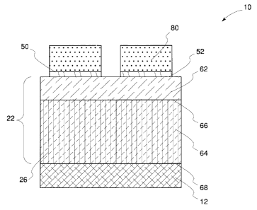
Figure 7 shows an exemplary single-substrate embodiment of the heat sink
assembly for
cooling a number of power devices.
While the above-identified drawing figures set forth alternative embodiments,
other
embodiments of the present invention are also contemplated, as noted in the
discussion. In all cases, this disclosure presents illustrated embodiments of
the
present invention by way of representation and not limitation. Numerous other
modifications and embodiments can be devised by those skilled in the art which
fall
within the scope and spirit of the principles of this invention.
3
CA 02704870 2010-05-20
225996-1
DETAILED DESCRIPTION
An apparatus 10 for cooling at least one heated surface 50 is described herein
with
reference to Figures 1-7. Apparatus 10, illustrated according to one
embodiment in
Figure 1, includes a base plate 12, which is shown in greater detail in Figure
2. According
to one embodiment illustrated in Figure 2, base plate 12 defines a number of
inlet
manifolds 16 and a number of outlet manifolds 18. The inlet manifolds 16 are
configured to receive a coolant 20, and the outlet manifolds 18 are configured
to
exhaust the coolant. As indicated in Figure 2, for example, inlet and outlet
manifolds
16, 18 are interleaved. As indicated in Figure 1, apparatus 10 further
includes at least
one substrate 22 having an inner surface 24 and an outer surface 52, the inner
surface
24 being coupled to base plate 12.
According to one embodiment as shown in Figure 4, the inner surface 24
features a
number of cooling fluid channels 26 configured to receive the coolant 20 from
inlet
manifolds 16 and to deliver the coolant to outlet manifolds 18. According to
one aspect,
cooling fluid channels 26 are oriented substantially perpendicular to inlet
and outlet
manifolds 16, 18. The outer surface 52 of substrate 22 is in thermal contact
with the
heated surface 50, as indicated in Figure 1. Apparatus 10 further includes an
inlet
plenum 28 configured to supply the coolant 20 to inlet manifolds 16 and an
outlet
plenum 40 configured to exhaust the coolant from outlet manifolds 18. As
indicated in
Figures 2 and 3, inlet plenum 28 and outlet plenum 40 are oriented in a plane
of base
plate 12.
Many coolants 20 can be employed for apparatus 10, and the invention is not
limited to a
particular coolant. Exemplary coolants include water, ethylene-glycol,
propylene-glycol,
oil, aircraft fuel and combinations thereof. According to a particular
embodiment, the
coolant is a single phase liquid. According to another embodiment, the coolant
is a multi-
phase liquid. In operation, the coolant enters the manifolds 16 in base plate
12 via the input
plenum 28 and flows through cooling fluid channels 26 before returning through
exhaust manifolds 18 and the output plenum 40. More particularly, coolant
enters
inlet plenum 28, whose fluid diameter exceeds that of the other channels in
apparatus 10,
4
CA 02704870 2010-05-20
225996-1
according to a particular embodiment, so that there is no significant pressure-
drop in the
plenum.
According to a particular embodiment, base plate 12 comprises a thermally
conductive
material. Exemplary materials include, without limitation, copper, Kovar,
Molybdenum,
titanium, ceramics, metal matrix composite materials and combinations thereof.
According to other embodiments, base plate 12 comprises a moldable, castable
or
machinable material.
Cooling fluid channels 26 encompass micro-channel dimensions to milli-channel
dimensions. Channels 26 may have, for example, a feature size of about 0.05mm
to
about 5.0mm according to some aspects of the invention. According to one
embodiment,
channels 26 are about 0.1 mm wide and are separated by a number of gaps of
about
0.2mm. According to yet another embodiment, channels 26 are about 0.3mm wide
and
are separated by a number of gaps of about 0.5mm. According to still another
embodiment, channels 26 are about 0.6mm wide and are separated by a number of
gaps
of about 0.8mm. Beneficially, by densely packing narrow cooling fluid channels
26,
the heat transfer surface area is increased, which improves the heat transfer
from the
heated surface 50.
Cooling fluid channels 26 can be formed with a variety of geometries.
Exemplary
cooling fluid channel 26 geometries include rectilinear and curved geometries.
The
cooling fluid channel walls may be smooth, for example, or may be rough. Rough
walls
increase surface area and enhance turbulence, increasing the heat transfer in
the
cooling fluid channels 26. For example, the cooling fluid channels 26 may
include
dimples to further enhance heat transfer. In addition, cooling fluid channels
26 may be
continuous, as indicated for example in Figure 4, or cooling fluid channels 26
may form
a discrete array 58, as exemplarily shown in Figure 5. According to a specific
embodiment, cooling fluid channels 26 form a discrete array 58 and are about 1
mm in
length and are separated by a gap of less than about 0.5 mm.
In addition to geometry considerations, dimensional factors also affect
thermal
performance. According to one aspect, manifold and cooling channel geometries
and
CA 02704870 2010-05-20
225996-1
dimensions are selected in combination to reduce temperature gradients and
pressure
drops.
According to one embodiment shown in Figure 6, substrate 22 includes at least
one
electrically conductive material 62 and at least one electrically isolating
material 64 such
as a suitable ceramic material. Exemplary ceramic bases include aluminum-oxide
(A1203), aluminum nitride (AN), beryllium oxide (BeO) and silicon nitride
(Si3N4).
Electrically conductive material 62 is bonded or brazed to only the topside
surface
66 of the electrically isolating material 64. According to one aspect,
electrically
conductive material 62 comprises molybdenum, kovar, metal matrix composite or
another suitable electrically conductive material that has a coefficient of
thermal
expansion equivalent to the electrically isolating material 64.
Since both the electrically conductive material 62 and the electrically
isolating
material 64 have substantially identical coefficients of thermal expansion,
out of
plane distortion is prevented during processing temperatures of fabricating
the
molybdenum or other electrically conductive material to the ceramic of other
electrically isolating material 64 or other temperature variations the
resultant
product would be exposed to during subsequent processing or n-use conditions.
The backside surface 68 of the electrically isolating material 64, without the
electrically conductive material 62, has the cooling fluid channels 26
fabricated
therein. The area(s) associated with the cooling fluid channels 26 lie
directly
beneath the heated surface(s) 50 that are subsequently attached to the
electrically
conductive material 62 on the topside surface 52 of the electrically isolating
material 64.
Beneficially, the completed substrate 22 can be attached to base plate 12
using any
one of a number of techniques, including brazing, bonding, diffusion bonding,
soldering, or pressure contact such as clamping. This provides a simple
assembly
process, which reduces the overall cost of the heat sink 10. Moreover, by
attaching the
substrate 22 to base plate 12, fluid passages are formed under the heated
surfaces 50,
enabling practical and cost-effective implementation of the cooling fluid
channel
cooling technology.
6
CA 02704870 2010-05-20
225996-1
It is noted that the embodiments described herein advantageously reduce the
thermal
resistance between the heated surface(s) 50 and the ultimate heatsink (fluid)
20. This
reduced temperature provides a more robust design of a corresponding power
electronics module such as the multiple semiconductor power device 80 module
depicted in Figure 7, by reducing the maximum operating temperature and
reducing
the minimum to maximum temperature excursions during power cycling during
device operation, thereby increasing device reliability. Further, the
embodiments
described herein advantageously place the cooling media 20 closer to the
heated
surface(s) 50 by locating the cooling fluid channels 26 in the electrically
isolating
material 64, thereby reducing the thermal resistance (junction to fluid) to
lower levels
than that achievable using known structures that employ metal layers on both
the
topside and bottomside surfaces of the substrate.
While only certain features of the invention have been illustrated and
described
herein, many modifications and changes will occur to those skilled in the art.
It is,
therefore, to be understood that the appended claims are intended to cover all
such
modifications and changes as fall within the true spirit of the invention.
7