Note: Descriptions are shown in the official language in which they were submitted.
CA 02704912 2012-06-25
HEATING ELEMENT INCORPORATING AN ARRAY
OF TRANSISTOR MICRO-HEATERS FOR DIGITAL IMAGE MARKING
BACKGROUND
[0001] The exemplary embodiments disclosed herein relate to heating
elements incorporating arrays of transistor micro-heaters for printing and
image
marking applications.
[0002] By way of background, current heat-based image marking engines
incorporate either thermal print head or laser heating technology. The thermal
print head must physically contact the surface in order to directly deliver
heat to
selected pixels, which restricts its application away from non-contact
required
environment, such as the nip region between two rollers. Also, the thermal
print
head is slow and energy inefficient. In the laser heating technology, optical
energy is absorbed and converted to heat, providing an ideal non-contact
heating
mechanism. The total power requirement for addressing a large-area surface at
reasonably high speed, however, is extremely high compared to common high
power laser systems. The lack of an inexpensive, powerful laser and the
complexity of optical systems make it nearly impossible to create a fast,
compact,
and cheap heat-based marking engine using current laser technology.
[0003] Accordingly, there is a need to overcome these and other problems of
the prior art to provide digital fusing subsystems that can reduce the amount
of
wasted heat, for example, by heating only those areas where the toner image
will
'be.
[0004] The following patents/applications are mentioned:
[0005] U.S. Patent No. 8,107,843, filed April 1, 2008, entitled DIGITAL
FUSER
CONCEPT USING MICRO HOTPLATE TECHNOLOGY, by Law;
[0006] U.S. Patent Publication Serial No. 2010/0085585, filed October 3,
2008, entitled DIGITAL IMAGING OF MARKING MATERIALS BY THERMALLY
INDUCED PATTERN-WISE TRANSFER, by Stowe, et al.; and
[0007] U.S. Patent Publication Serial No. 2010/0251914, filed April 1,2009,
entitled IMAGING MEMBER, by Zhou, et al.
1
CA 02704912 2012-06-25
BRIEF DESCRIPTION
[0008] Transistors have been used as micro-heaters in chemical sensor
application. Transistor heaters with a dimension of 200 pm fabricated by
conventional CMOS techniques on silicon wafers can heat up to 350 C with
thermal response time in the order of milliseconds. The exemplary embodiments
disclosed herein leverage transistor heating technology to create micro-heater
arrays as the digital heating element for various marking applications. The
transistor heaters are typically fabricated either on a thin flexible
substrate or on
an amorphous silicon drum and embedded below the working surface. Matrix
drive methods may be used to address each individual micro-heater and deliver
heat to selected surface areas. Depending on different marking applications,
the
digital heating element may be used to selectively tune the wettability of
thermo-
sensitive coating, selectively change the ink rheology, selectively remove
liquid
from the surface, selectively fuse/fix toner/ink on the paper.
[0009] In one embodiment, an image marking system is provided. The image
marking system includes one or more digital heating elements, the digital
heating
element comprising a micro-heater array having thermally isolated and
individually addressable transistor micro-heaters that can attain a
temperature up
to approximately 200 C from approximately 20 C within a few milliseconds.
[0010] In another embodiment, a method of forming an image is provided.
The method comprises: forming a toner or ink image on an imaging member;
and providing a fixing subsystem comprising one or more digital heating
elements, wherein the digital heating element comprises a micro-heater array
having thermally isolated and individually addressable transistor micro-
heaters; selectively heating one or more transistor micro-heaters that
correspond to the toner or ink image to a temperature in the range of
approximately 20 C to approximately 200 C in a few milliseconds; and
feeding the media through the fuser subsystem to fix the toner or ink image
on the media.
[0011] In yet another embodiment, a method of forming an ink image is
provided. The method comprises: feeding a media in a digital lithographic
2
CA 02704912 2010-05-21
development subsystem comprising an imaging member, wherein the
imaging member comprises a wettability switchable surface and one or more
digital heating elements that comprise an array of transistor micro-heaters,
wherein each micro-heater is thermally isolated and individually addressable;
changing the surface of the imaging member on the image areas from ink-
repelling state to ink-attracting state by heating one or more micro-heaters
that correspond to the image areas to a temperature in the range of
approximately 20 C to approximately 200 C in a few milliseconds; forming an
ink image by applying ink to the image areas that are ink-attracting;
transferring the ink image from the imaging member onto the media; and
transporting the media to a fixing station.
[0012] In yet another embodiment, a method of forming an ink image is
provided. The method comprises: feeding a media in a digital lithographic
development subsystem comprising an imaging member, wherein the
imaging member comprises a wettability switchable surface and one or more
digital heating elements that comprise an array of transistor micro-heaters,
wherein each micro-heater is thermally isolated and individually addressable;
applying a thin fountain solution film on the imaging member; removing
fountain solution from the image areas by heating one or more micro-heaters
that correspond to the image areas to a temperature in the range of
approximately 20 C to approximately 200 C in a few milliseconds; forming a
ink image by applying ink to the image areas where fountain solution is
removed; transferring ink image onto the media; and transporting the media
to a fixing station.
[0013] In yet another embodiment, a method of forming an ink image
comprises: feeding a media in a digital lithographic development subsystem
comprising an imaging member, wherein the imaging member comprises a
wettability switchable surface and one or more digital heating elements that
comprise an array of transistor micro-heaters, wherein each micro-heater is
thermally isolated and individually addressable; applying a waterless
lithographic ink film on the imaging member; changing the rheological
properties of the waterless lithographic ink on the image areas by heating
one or more micro-heaters that correspond to the image areas to a
temperature in the range of approximately 20 C to approximately 200 C in a
3
CA 02704912 2012-06-25
few milliseconds; transferring the rheology-modified ink image from imaging
member onto the media; and transporting the media to a fixing station.
[0013a] In accordance with another aspect, there is provided an image marking
system comprising: one or more digital heating elements, the digital heating
element comprising a micro-heater array having thermally isolated and
individually addressable transistor micro-heaters that can attain a
temperature up
to approximately 200 C from approximately 20 C within a few milliseconds.
[0013b] In accordance with a further aspect, there is provided a method of
forming an image comprising: forming a toner or ink image on an imaging
member; and providing a fixing subsystem comprising one or more digital
heating
elements, wherein the digital heating element comprises a micro-heater array
having thermally isolated and individually addressable transistor micro-
heaters;
selectively heating one or more transistor micro-heaters that correspond to
the
toner or ink image to a temperature in the range of approximately 20 C to
approximately 200 C in a few milliseconds; and feeding the media through the
fuser subsystem to fix the toner or ink image on the media.
[0013c] In accordance with another aspect, there is provided a method of
forming an ink image comprising: feeding a media in a digital lithographic
development subsystem comprising an imaging member, wherein the imaging
member comprises a wettability switchable surface and one or more digital
heating elements that comprise an array of transistor micro-heaters, wherein
each micro-heater is thermally isolated and individually addressable; changing
the surface of the imaging member on the image areas from ink-repelling state
to
ink-attracting state by heating one or more micro-heaters that correspond to
the
image areas to a temperature in the range of approximately 20 C to
approximately 200 C in a few milliseconds; forming an ink image by applying
ink
to the image areas that are ink-attracting; transferring the ink image from
the
imaging member onto the media; and transporting the media to a fixing station.
[0013d] In accordance with a further aspect, there is provided a method of
forming an ink image comprising: feeding a media in a digital lithographic
development subsystem comprising an imaging member, wherein the imaging
member comprises a wettability switchable surface and one or more digital
4
CA 02704912 2012-06-25
heating elements that comprise an array of transistor micro-heaters, wherein
each micro-heater is thermally isolated and individually addressable; applying
a
thin fountain solution film on the imaging member; removing fountain solution
from the image areas by heating one or more micro-heaters that correspond to
the image areas to a temperature in the range of approximately 20 C to
approximately 200 C in a few milliseconds; forming a ink image by applying ink
to
the image areas where fountain solution is removed; transferring ink image
onto
the media; and transporting the media to a fixing station.
[0013e] In accordance with another aspect, there is provided a method of
forming an ink image comprising: feeding a media in a digital lithographic
development subsystem comprising an imaging member, wherein the imaging
member comprises a wettability switchable surface and one or more digital
heating elements that comprise an array of transistor micro-heaters, wherein
each micro-heater is thermally isolated and individually addressable; applying
a
waterless lithographic ink film on the imaging member; changing the
rheological
properties of the waterless lithographic ink on the image areas by heating one
or
more micro-heaters that correspond to the image areas to a temperature in the
range of approximately 20 C to approximately 200 C in a few milliseconds;
transferring the rheology-modified ink image from imaging member onto the
media; and transporting the media to a fixing station.
[0013f] In accordance with a further aspect, there is provided an image
marking system comprising: one or more digital heating elements, the digital
heating element comprising a micro-heater array having thermally isolated and
individually addressable transistor micro-heaters that can attain a
temperature up
to approximately 200 C from approximately 20 C within a few milliseconds;
wherein the transistor micro-heater comprises a heating transistor and a
switching transistor that controls the gate voltage of the heating transistor,
and
the temperature of the transistor micro-heater is adjustable via the source-
gate
voltage of the heating transistor, and further wherein the micro-heater array
further comprises a data driver providing data drive lines connected to the
source
electrodes of the switching transistors and a scan driver providing scan drive
4a
CA 02704912 2012-06-25
lines connected to the gate electrodes of the switching transistors optionally
wherein the micro-heater array is addressed by a passive matrix drive.
[0013g] In accordance with another aspect, there is provided an image marking
system comprising: one or more digital heating elements, the digital heating
element comprising a micro-heater array having thermally isolated and
individually addressable transistor micro-heaters that can attain a
temperature up
to approximately 200 C from approximately 20 C within a few milliseconds;
wherein the transistor micro-heater comprises a heating transistor and a
switching transistor that controls the gate voltage of the heating transistor,
and
the temperature of the transistor micro-heater is adjustable via the source-
gate
voltage of the heating transistor, and further wherein each micro-heater in
the
array further comprises a capacitor that holds the source-gate voltage of the
heating transistor after the micro-heater is addressed, and micro-heater array
is
addressed by a passive matrix drive.
[0013h] In accordance with a further aspect, there is provided a method of
forming an image comprising: forming a toner or ink image on an imaging
member; providing a fixing subsystem comprising one or more digital heating
elements, wherein the digital heating element comprises a micro-heater array
having thermally isolated and individually addressable transistor micro-
heaters;
wherein the transistor micro-heater comprises a heating transistor and a
switching transistor that controls the gate voltage of the heating transistor,
and
the temperature of the transistor micro-heater is adjustable via the source-
gate
voltage of the heating transistor, and further wherein the micro-heater array
further comprises a data driver providing data drive lines connected to the
source
electrodes of the switching transistors and a scan driver providing scan drive
lines connected to the gate electrodes of the switching transistors optionally
wherein the micro-heater array is addressed by a passive matrix drive;
selectively
heating one or more transistor micro-heaters that correspond to the toner or
ink
image to a temperature in the range of approximately 20 C to approximately
200 C in a few milliseconds; and feeding the media through the fuser subsystem
to fix the toner or ink image on the media.
4b
CA 02704912 2012-06-25
[0013i] In accordance with another aspect, there is provided a method of
forming an image comprising: forming a toner or ink image on an imaging
member; providing a fixing subsystem comprising one or more digital heating
elements, wherein the digital heating element comprises a micro-heater array
having thermally isolated and individually addressable transistor micro-
heaters;
wherein the transistor micro-heater comprises a heating transistor and a
switching transistor that controls the gate voltage of the heating transistor,
and
the temperature of the transistor micro-heater is adjustable via the source-
gate
voltage of the heating transistor, and further wherein each micro-heater in
the
array further comprises a capacitor that holds the source-gate voltage of the
heating transistor after the micro-heater is addressed, and micro-heater array
is
addressed by a passive matrix drive; selectively heating one or more
transistor
micro-heaters that correspond to the toner or ink image to a temperature in
the
range of approximately 20 C to approximately 200 C in a few milliseconds; and
feeding the media through the fuser subsystem to fix the toner or ink image on
the media.
BRIEF DESCRIPTION OF THE DRAWINGS
[0014] FIG. 1 is a cross-sectional view of a micro-hotplate with an
integrated
pMOS transistor heater;
[0015] FIG. 2 is a close-up of the inner section of the micro-hotplate;
[0016] FIG. 3 is a schematic diagram of a resistive heating element;
[0017] FIG. 4 is a schematic diagram of a transistor heating element;
[0018] FIG. 5 is a graph showing that the membrane temperature of the
transistor heater-based chemical sensor (FIG. 1) varies as a function of
source-
gate voltage for different source-drain voltages;
[0019] FIG. 6 is a schematic diagram of an array of 10 x 10 transistor
micro-
heaters in accordance with aspects of the exemplary embodiments;
[0020] FIG. 7 is a close up of a transistor micro-heater from FIG. 6;
4c
CA 02704912 2012-06-25
[0021] FIG. 8 is a cross-section view of an axis-symmetric design of a
single
transistor micro-heater in accordance with aspects of the exemplary
embodiments;
[0022] FIG. 9 is a schematic diagram showing a simplified matrix drive for
addressing individual transistor micro-heater;
[0023] FIG. 10 is a zoom-in of a single micro-heater design with passive
matrix drive;
[0024] FIG. 11 is a zoom-in of a single micro-heater design with active
matrix drive;
[0025] FIG. 12 schematically illustrates an exemplary printing apparatus;
[0026] FIG. 13 schematically illustrates an exemplary fuser subsystem of a
printing apparatus, according to various embodiments of the present
teachings;
[0027] FIG. 14 schematically illustrates another exemplary fuser subsystem
of a printing apparatus, according to various embodiments of the present
teachings;
[0028] FIG. 15 schematically illustrates a cross section of an exemplary
fuser member, according to various embodiments of the present teachings;
and
4d
CA 02704912 2010-05-21
[0029] FIG. 16 schematically illustrates a cross section of another
exemplary
fuser member, according to various embodiments of the present teachings.
DETAILED DESCRIPTION
[0030] A schematic view of an example of a prior art micro-hotplate-based
chemical sensor 10 with an integrated PMOS transistor heater 12 is shown in
FIG. 1. In order to ensure a good thermal insulation, only the dielectric
layers of
the CMOS process form the membrane 14. The inner section 16 of the dielectric
membrane 14 includes an n-well silicon island 17 (e.g., 300 pm base length)
underneath the dielectric layers (e.g., 500 x 500 pm). The n-well 17 is
electrically
insulated and serves as heat spreader owing to the good thermal conductivity
of
silicon. It also hosts the pMOS transistor heating element 12, which includes
p-
diffusion 18 and a gate 19 (e.g., 5pm gate length and 710 pm overall gate
width).
A special ring-shape transistor arrangement improves homogeneous heat
distribution. A poly-silicon resistor 20 is used to measure the temperature on
the
micro-micro-heater 10. The resistance of the nanocrystalline SnO thick-film
layer
22 is read out by means of two noble-metal-coated (Pt) electrodes 24 for
detecting the molecule induced resistance change in SnO film.
[0031] The device fabrication relies on an industrial 0.8-pm CMOS process
(austriamicrosystems, Unterpremstatten, Austria) combined with post-CMOS
micromachining steps. The inner section 16 of the membrane 14 (e.g., 500 x 500
pm2) exhibits an octagonal-shape n-well silicon island 18 (e.g., 300 pm base
length). The octagonal shape provides a comparatively large distance between
the heated membrane area and the cold bulk chip [close up in FIG. 2].
Furthermore, this symmetric shape promotes homogeneous heat distribution. A
resistive polysilicon temperature sensor 20 (connected to circuitry) that
measures
membrane temperature (TM) is located at the center. Bulk silicon 30 is not
part of
the electronic device, but it does provide mechanical support for the
suspended
micro-micro-heater.
[0032] The thermal efficiency is 5.8 C/mW and the thermal time constant is
9
ms for this specific transistor heater. Depending on the size, geometry,
arrangement, and material of a transistor heater, its properties could vary a
lot.
In general, this type of transistor heater can heat up to 350 C with thermal
response time in the order of millisecond.
CA 02704912 2010-05-21
[0033] Following the design of the digital heating element based on
resistive
heater arrays in prior art, a new digital heating element based on transistor
micro-
heater arrays consisting of thousands to millions of micron-sized transistor
heaters was developed. There are some differences between these two types of
micro-heaters. The resistive heater can heat up to 1000 C if tungsten is used
as
the resistive material. By contrast, the transistor heater fabricated on a
silicon
wafer can only reach about 350 C because the transistor will burn out above
this
temperature.
[0034] Schematic diagrams of the two micro-heating schemes are shown in
FIG. 3 (resistive heating) and in FIG. 4 (transistor heating). FIG. 3 shows a
basic
unit of resistive heating array including a heating resistor (RHEAT), a power
transistor (QpowER), and a temperature monitoring resistor (RTEmp). The power
transistor is required for switching the micro-heater by controlling the gate
voltage
(Ucontroi) of the power transistor. The supplied voltage (Usuggiy) is split
between the
heating resistor and the power transistor. The temperature monitoring resistor
may be added to the basic unit for feedback control on temperature. FIG.4
shows a basic unit of a transistor heating array, including a heating
transistor
(QHEAT) and a temperature monitoring resistor (RTEmp). Similarly, switching of
the
micro-heater is controlled by the gate voltage (Ucon )
trol,=
[0035] Generally, the highest temperature is limited for all types of
transistor
heaters. However, the transistor heaters are more energy efficient since
resistive
heaters require power transistors to switch on/off and a massive fraction of
the
overall power is dissipated on power transistors, as illustrated in FIG. 3.
Furthermore, the resistance of the heating transistor varies with its source-
gate
voltage, thus leading to a linear dependence of the micro-heater temperature
TM
on the transistor source-gate voltage Usg for Usg above the threshold voltage,
as
shown in FIG. 5. This provides a simple approach to control the temperature of
each individual micro-heater.
[0036] It is possible to leverage and extend the transistor micro-heater
technology for different marking applications, such as direct marking in
digital
lithographic press and transfuse/transfix device in dry and liquid xerography.
This involves the construction of a large area heating surface consisting of
an
array of transistor micro-heaters with the size from several microns to
hundred of
6
CA 02704912 2010-05-21
microns using a combination of CMOS, printable electronic and nanofabrication
technologies.
[0037] FIG. 6 is a top view of an exemplary example of a digital heating
element (or device) 100 with a 10 x 10 array of transistor micro-heaters 102
(electrodes and wires are removed for better viewing). Each micro-heater 102
of
the array of heaters can be thermally isolated and can be individually
addressable, and each micro-heater 102 can be configured to attain a
temperature of up to approximately 200 C from approximately 20 C in a time
frame of milliseconds. In some embodiments, the time frame of milliseconds can
be less than about 100 milliseconds. In other embodiments, the time frame of
milliseconds can be less than about 50 milliseconds. Yet, in some other
embodiments, the time frame of milliseconds can be less than about 10
milliseconds. The phrase "individually addressable" as used herein means that
each micro-heater 102 of the array of micro-heaters can be identified and
manipulated independently of its surrounding heaters, for example, each micro-
heater 102 can be individually turned on or off or can be heated to a
temperature
different from its surrounding heaters. However, in some embodiments, instead
of addressing the micro-heaters individually, a group of micro-heaters
including
two or more heaters can be addressed together, i.e., a group of micro-heaters
can be turned on or off together or can be heated to a certain temperature
together, different from the other micro-heaters or other groups of micro-
heaters.
[0038] FIG. 7 is a close-up showing the source 104, the channel 106 and the
drain 108 of the transistor micro-heater 102. Though the transistors 102 in
this
example have a circular shape, other shapes can be made as well (e.g.,
polygon,
ribbon, and spiral). The transistor micro-heater array 100 is directly
embedded
below the work surface 110 for fast and efficient heating.
[0039] A cross-section of this design is shown in FIG. 8. In order to
generate
and distribute heat uniformly, an axis symmetric shape may be chosen for the
transistor micro-heater design. But the actual micro-heater 150 is not limited
to
axis symmetric shapes, as long as heat distribution is homogeneous across the
top surface (the working surface) 151. The transistor micro-heater 150
includes a
ring-shaped bottom gate 152, a ring-shaped source 154 connected to an upper
conductive metal layer 156, and a round drain 158 connected to a lower
conductive metal layer 160. The use of metal layers has at least two purposes:
7
CA 02704912 2010-05-21
(1) it reduces power wasted on the wire interconnections since a huge current
must be supplied to each transistor, and (2) it helps to distribute heat
uniformly
across the surface. The semiconductor layer 162 is several microns thick and
is
composed of either inorganic or organic materials with high electron mobility
(>
cm2N.$). The substrate layer 164 is generally either a flexible plastic with
very low thermal conductivity or a thermal insulating material coated on a
drum.
Basically, any low thermal conductivity materials (k < 1 Wm-1K1) can be used
as
a substrate layer. The thickness of the substrate layer 164 is generally
between
50 pm and several millimeters. The relative thickness of the upper and lower
conductive layers 156, 160 and the upper and lower electrically insulating
dielectric layers 166, 168 is in the neighborhood of only a few hundreds of
nanometers. Thus, with this design it is now possible to provide a constant
voltage between the upper metal layer (source) and the lower metal layer
(drain)
and simply change the gate voltage to adjust heating power and the
temperature.
[0040] In certain embodiments, the top surface 151 in FIG. 8 may comprise a
thermal spreading layer. The thickness of the thermal spreading layer can be
from about 5 pm to about 50 pm, and in some cases from about 10 pm to about
30 pm. In some embodiments, the thermal spreading layer can include thermally
conductive fillers disposed in a polymer. In various embodiments, the
thermally
conductive fillers can be selected from the group consisting of graphites;
graphenes; carbon nanotubes; micron to submicron sized metal particles, such
as, for example, Ni, Ag, and the like; and micron to submicron sized ceramic
fillers, such as SiC, A1203, and AIN. In other embodiments, the polymer in
which
the thermally conductive fillers are disposed can be selected from the group
consisting of polyimides, silicones, fluorosilicone, and fluoroelastomers.
However, one of ordinary skill in the art may choose any suitable thermally
conductive filler disposed in any suitable polymer
[0041] A combination of photolithography, printed electronics, and
nanofabrication technologies can be used to fabricate the transistor micro-
heater
arrays. The fabrication process depends on the type of materials used and the
type of substrate. For example, if the micro-heater array is fabricated on a
flexible substrate, photolithography technology may be used to create
insulating
layers, metal layers, and interconnections while printed electronics and
nanofabrication technologies may be used to create semiconductor layers.
8
CA 02704912 2010-05-21
Electron mobility is a key requirement for semiconductor materials used in
transistor micro-heaters. The amorphous silicon-based thin film transistors
cannot generate enough heating power because the maximum current is limited
by amorphous silicon's low electron mobility (1 cm2V1S-1), and a polysilicon-
like
material is required for the transistor channel due to their higher electron
mobility
(>30 cm2V1s-) i..
One possible way of making a high performance transistor
channel is to use known excimer laser-induced crystallization or metal-induced
crystallization or other similar crystallization methods to crystallize
deposited
amorphous semiconductor materials, such as amorphous silicon and amorphous
germanium. Metal-induced crystallization (MIC) is a method by which amorphous
silicon, or a-Si, can be turned into polycrystalline silicon at relatively low
temperatures. In MIC an amorphous Si film is deposited onto a substrate and
then capped with a metal, such as aluminum. The structure is then annealed at
temperatures between 150 C and 400 C, thus causing the a-Si films to be
transformed into polycrystalline silicon. ZnO thin film is also a promising
high
electron mobility material that can be deposited on flexible substrates and
curved
surfaces.
[0042]
Passive matrix drive or active matrix drive can be used to address each
individual micro-heater, as illustrated in FIGS. 9-11 Active matrix drive and
passive matrix drive are two pixel-addressable mechanisms used in LCD
technology. An exemplary digital heating element (or device) 180 comprising a
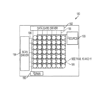
x 10 array of transistor micro-heaters 181 is shown in FIG. 9. The transistor
micro-heater 181 generally has a length and width in between 10 pm and 500
pm. The data driver 182 provides 10 data drive lines 188 and the scan driver
184
provides 10 scan drive lines 186. At each intersection of data drive lines 188
and
scan drive lines 186 is a heating transistor 193 and its switching transistor
191 as
shown in FIG. 10 and 11. The source electrodes 194 and drain electrodes 195 of
the heating transistors 193 are connected to the same Vsource 189 and VDrain
190,
respectively. Each switching transistor 191 has a gate terminal connected to a
scan drive line 186, a source terminal connected to a data drive line 188, and
a
drain terminal connected to the gate electrode 196 of the heating transistor
193.
Each heating transistor 193 is addressed by activating its switching
transistor 191
via its scan drive line 186 and sending control signal to its gate electrode
196 via
9
CA 02704912 2010-05-21
,
,
,
its data drive line 188. The selection of passive matrix drive or active
matrix drive
depends on the application requirement.
[0043] In passive matrix drive (see FIG. 10), the scan driver 184 scans
all
micro-heaters 181 row by row and in each time interval only one row of
switching
transistors 191 are activated so that data driver 182 can change the gate 196
voltage of individual heating transistor 193 through data drive lines 188.
However, the heating transistor 193 is turned off as soon as the scan driver
moves to the next row, which is a passive response to addressing signals. In
this
passive drive mechanism, no more than one row of micro-heaters 181 can
operate in each time inverval. Thus, passive matrix drive works better for
relatively small micro-heater arrays (less than 1000 rows). In contrast,
active
matrix drive (see FIG. 11) is preferred for operating fast (scanning rate
greater
than 20 Hz) and large area transistor arrays (more than 1000 rows). As
indicated
in FIG. 11, an extra capacitor 192 is inserted with one end connected to
Vsource
and other end connected to the gate electrode 196 of the heating transistor
193.
The addressing mechanism of active matrix drive is similar to passive matrix
drive except that the capacitor 192 can actively maintain the source-gate
voltage,
and consequently operating status of the heating transistor 193, even after
scan
driver moves to another row. Therefore, more than one row of micro-heaters 181
may be operating at the same time, and, if needed, each individual micro-
heater
can be turned off by another addressing signal via its scan drive line 186 and
data drive line 188.
[0044] The digital heating element comprising a transistor micro-heater
array
described herein can be integrated into different types of marking systems for
various applications. In one example, a fuser subsystem with integrated
digital
heating element in an electrophotographic printer can selectively fuse or fix
toner
or liquid toner image on a printing media.
[0045] FIG. 12 schematically illustrates an exemplary printing apparatus
200,
which includes an electrophotographic photoreceptor 201 and a charging station
202 for uniformly charging the electrophotographic photoreceptor 201. The
electrophotographic photoreceptor 201 can be a drum photoreceptor as shown in
FIG. 1 or a belt photoreceptor (not shown). The printing apparatus 200 also
includes an imaging station 203 where an original document (not shown) can be
exposed to a light source (also not shown) for forming a latent image on the
CA 02704912 2010-05-21
electrophotographic photoreceptor 201. The printing apparatus 200 further
includes a development subsystem 204 for converting the latent image to a
visible image on the electrophotographic photoreceptor 201 and a transfer
subsystem 205 for transferring the visible image onto a media and a fuser
subsystem 206 for fixing the visible image onto a media.
[0046] The fuser subsystem 206 includes one or more digital heating
elements 180 as shown in FIG. 9. The fuser subsystem 206 can include one or
more of a fuser member, pressure members, external heat rolls, oiling
subsystems, and transfix rolls. FIG. 15 shows an exemplary fuser member 410
including a digital heating element 180 disposed over a substrate 402 and a
toner
release layer 406 disposed over the digital heating element 180. The substrate
402 can be a high temperature plastic substrate such as polyimide or PEEK. The
thickness of the substrate 402 can be from about 50 pm to about 150 pm, and in
some cases from about 65 pm to about 85 pm. The toner release layer 406 is
typically a single layer including materials such as silicone, fluorosilicone
or
fluoroelastomer. The thickness of the toner release layer 406 can be from
about
100 pm to about 500 pm, and in some cases from about 150 pm to about 250
pm. The toner release layer 406 can also be a double layer structure including
a
fluoroelastomer layer disposed over a silicone rubber layer. In some other
embodiments, the toner release layer 406 can be a double layer structure
including a thermoplastic layer such as PTFE or PFA disposed over a silicone
rubber layer. The total thickness of the double layer structure of the toner
release
layer 406 can be from about 100 pm to about 500 pm, and in some cases from
about 150 pm to about 250 pm, with the top layer thickness from about 20 pm to
about 30 pm. In some embodiments, an electrically insulating layer 405 can be
disposed over the digital heating element 180 including an array of micro-
heaters
181, as shown in FIG. 16. In various embodiments, the electrically insulating
layer 405 can include any suitable material such as, for example, silicon
oxide,
polyimide, silicone rubber, fluorosilicone, and a fluoroelastomer. The
thickness
of the electrically insulating layer 405 can be from about 10 pm to about 50
pm,
and in some cases from about 20 pm to about 30 pm. In certain embodiments, a
thermal spreading layer 407 can be disposed over the electrically insulating
layer
405, as shown in FIG. 16. The thickness of the thermal spreading layer 407 can
be from about 10 pm to about 50 pm, and in some cases from about 20 pm to
11
CA 02704912 2010-05-21
about 30 pm. In some embodiments, the thermal spreading layer 407 can
include thermally conductive fillers disposed in a polymer. The thermally
conductive fillers can be selected from the group consisting of graphites;
graphenes; carbon nanotubes; micron to submicron sized metal particles, such
as, for example, Ni, Ag, and the like; and micron to submicron sized ceramic
fillers, such as, for example, SiC, A1203, and AIN. The polymer in which the
thermally conductive fillers are disposed can be selected from the group
consisting of polyimides, silicones, fluorosilicone, and fluoroelastonners.
However, one of ordinary skill in the art may choose any suitable thermally
conductive filler disposed in any suitable polymer.
[0047] Referring back to the digital heating element 180 disposed over the
substrate 402, the digital heating elements 180 can include an array of micro-
heaters 181, as shown in FIG. 9. Each micro-heater 181 of the array of micro-
heaters can be thermally isolated and can be individually addressable, and
wherein each micro-heater 181 can be configured to attain a temperature of up
to
approximately 200 C from approximately 20 C in a time frame of milliseconds.
In some embodiments, the time frame of milliseconds can be less than about 100
milliseconds. In other embodiments, the time frame of milliseconds can be less
than about 50 milliseconds. Yet, in some other embodiments, the time frame of
milliseconds can be less than about 10 milliseconds. The phrase "individually
addressable" as used herein means that each micro-heater 181 in the array can
be identified and manipulated independently of its surrounding micro-heaters,
for
example, each micro-heater 181 can be individually turned on or off or can be
heated to a temperature different from its surrounding micro-heaters. However
in
some embodiments, instead of addressing the micro-heaters individually, a
group
of micro-heaters including two or more micro-heaters can be addressed
together,
that is, a group of micro-heaters can be turned on or off together or can be
heated to a certain temperature together, different from the other micro-
heaters
or other groups of micro-heaters. For example, in the case of printing text
with a
certain line spacing and margins, the micro-heaters corresponding to the text
can
be heated to a certain temperature to fuse the toner, but the micro-heaters
corresponding to the line spacing between the text and the margins around the
text can be turned off.
12
CA 02704912 2010-05-21
,
[0048] FIG. 13 schematically illustrates an exemplary fuser subsystem 209
of
a xerographic printer. The fuser subsystem 209 includes a fuser member 210
and a rotatable pressure member 212 that can be mounted forming a fusing nip
211. A media 220 carrying an unfused toner image can be fed through the fusing
nip 211 for fusing. The pressure member 212 can be a pressure roll (as shown
in
FIG. 2) or a pressure belt (not shown). The fuser subsystem 209 can also
include an oiling subsystem 218 to oil the surface of the fuser member 210 to
ease the removal of residual toner. The fuser subsystem 201 can further
include
external heat rolls 214 to provide additional heat source and cleaning
subsystem
216. In various embodiments, one or more of fuser member 210, pressure
members 212, external heat rolls 214, and oiling subsystem 218 can include
digital heating element 180. In various embodiments, the digital heating
elements 180 can be used as a heat source and can be disposed in the pressure
member 212, the external heat rolls 214, and the oiling subsystem 218 in a
configuration similar to that for the fuser member 410 as disclosed above and
shown in FIGS. 15 and 16.
[0049] FIG. 14 schematically illustrates an alternative fuser subsystem
301 of
a solid inkjet printer. The fuser subsystem 301 as illustrated in FIG. 3 can
include
a solid ink reservoir 330. The solid ink can be melted by heating to a
temperature
of about 150 C and the melted ink 332 can then be ejected out of the solid
ink
reservoir 330 onto a transfix roll 310. In various embodiments, the transfix
roll
310 can be kept at a temperature in the range of about 70 C to about 130 C
to
prevent the ink 332 from solidifying. The transfix roll can be rotated and the
ink
can be deposited onto a media 320, which can be fed through a fusing nip 321
between the transfix roll 310 and a pressure roll 312. The pressure roll 312
can
be kept at a room temperature, or it can be heated to a temperature in the
range
of about 50 C to about 100 C. In various embodiments, the digital heating
elements 180 can be used as a heat source and can be disposed in the transfix
roll 310 and/or the pressure roll 312 in a configuration similar to that for
the fuser
member 410, 410' as disclosed above and shown in FIGS. 15 and 16. In various
embodiments, the inclusion of the digital heating element 180 in the transfix
roll
310 can allow heating only those parts of the transfix roll 310 that includes
ink
and correspond to the ink image by selectively addressing one or more micro-
heaters 181 of the array of micro-heaters 181.
13
CA 02704912 2010-05-21
[0050] A method of forming an image may thus include providing an imaging
station for forming a latent image on an electrophotographic photoreceptor.
The
method may also include providing a development subsystem for converting the
latent image to a toner image on the electrophotographic photoreceptor. The
method can further include providing a fuser subsystem including one or more
heating elements for fixing the toner image onto a media, each of the one or
more digital heating elements can include an array of micro-heaters, wherein
each micro-heater of the array of micro-heaters can be thermally isolated and
can
be individually addressable. In certain embodiments, each micro-heater can be
configured to attain a temperature of up to approximately 200 C from
approximately 20 C in a time frame of milliseconds. In some embodiments, the
step 663 of providing a fuser assembly can include providing the fuser
assembly
in a roller configuration. In other embodiments, the step of providing a fuser
assembly can include providing the fuser assembly in a belt configuration. In
some other embodiments, the step of providing a fuser subsystem can include
providing one or more of a fuser member, pressure members, external heat
rolls,
oiling subsystem, and transfix roll. In various embodiments, the method 600
can
also include selectively heating one or more micro-heaters that correspond to
the
toner image to a temperature in the range of approximately 20 C to
approximately 200 C in a time frame of milliseconds and feeding the media
through the fuser subsystem to fix the toner image onto the media. In certain
embodiments, the step of selectively heating one or more micro-heaters that
correspond to the toner image can include selectively heating a plurality of
group
of micro-heaters, wherein each group of micro-heaters can be individually
addressable. In various embodiments, the step of selectively heating one or
more micro-heaters can include heating a first group of micro-heaters to a
first
temperature, a second group of micro-heaters to a second temperature, the
second temperature being different from the first temperature, and so on. One
of
ordinary skill in the art would know that there can be numerous reasons to
heat a
first group of micro-heaters to a first temperature, a second set of micro-
heaters
to a second temperature, the second temperature being different from the first
temperature, and so on. Exemplary reasons can include, but are not limited to
increasing energy efficiency and improving image quality. For example, in a
given media, such as a paper, one can heat certain areas to a higher
14
CA 02704912 2010-05-21
temperature if those areas have higher toner coverage such as, due to graphic
images. Also, one can heat some areas on a media to a higher temperature to
increase the glossiness. In some embodiments, the method can further include
selectively pre-heating only those parts of the media that correspond to the
toner
image by selectively heating one or more micro-heaters of the array of micro-
heaters that correspond to the toner image. In certain embodiments, the method
can further include adjusting an image quality of the image on the media by
selectively heating only those parts of the media that corresponds to the
image
by selectively heating one or more micro-heaters of the array of micro-heaters
that correspond to the image.
[0051] According to various embodiments, there is a marking method
including feeding a media in a marking system, the marking system including
one
or more digital heating elements, each of the one or more digital heating
elements including an array of micro-heaters, wherein each micro-heater can be
thermally isolated and can be individually addressable. The marking method can
also include transferring and fusing an image onto the media by heating one or
more micro-heaters that correspond to the toner image to a temperature in the
range of approximately 20 C to approximately 200 C in a time frame of
milliseconds. The marking method can further include transporting the media to
a finisher. In various embodiments, the step of transferring and fusing an
image
onto the media by heating one or more micro-heaters that correspond to the
toner image can include heating a first set of micro-heaters corresponding to
a
first region of the toner image to a first temperature, a second set of micro-
heaters corresponding to a second region of the toner image to a second
temperature, wherein the second temperature can be different from the first
temperature, and so on. In some embodiments, the marking method can also
include selectively pre-heating only those parts of a media that correspond to
the
toner image by selectively heating one or more micro-heaters of the array of
micro-heaters that correspond to the toner image. In certain embodiments, the
marking method can also include adjusting an image quality of the image on the
media by selectively heating only those portions of the media that corresponds
to
the image by selectively heating one or more micro-heaters of the array of
micro-
heaters that correspond to the image.
CA 02704912 2010-05-21
,
[0052] The techniques described herein may also be used to print variable
data with an offset lithographic printer. Variable-data printing is a form of
on-
demand printing in which elements such as text, images may be changed from
one page to the next, without stopping or slowing down the printing process.
The
conventional lithographic printing techniques include a plate with fixted
hydrophilic and hydrophobic patterns. The plate is wet with fountain solution
and
then inked and the ink image is transferred to a media such as paper. The
fountain solution coats the hydrophilic portions of the plate and prevents ink
from
being deposited on those areas of the plate. In lithographic printing the
plate must
be changed whenever the printing content is changed. The digital heating
elements described herein can be used in digital lithographic printing
techniques
that can print variable data without changing plates. In one embodiment, the
plate is coated with a thermo-responsive wettability switchable material,
under
which are digital heating elements. The local surface wettability of the plate
can
be switched between ink-attracting state at one temperature and ink-repelling
state at a different temperature. The digital heating element can selectively
heat
a thermo-responsive surface to form ink-attracting image area upon which ink
can adhere. In another embodiment, the digital heating element is embedded in
a blank plate to image-wise remove the thin fountain solution film to form a
negative, ink-repelling image. In another embodiment, a blank silicone plate
with
embedded digital heating element can image-wise heat the waterless
lithographic
ink to change ink rheology so that ink transfer from silicone plate to the
substrate
in heated areas.
[0053] In the above applications, if differential heating is required,
the digital
heating element can operate in such a way as to heat a first set of transistor
micro-heaters to a first temperature, a second set of transistor micro-heaters
to a
second temperature, wherein the second temperature is different from the first
temperature, and so on.
[0054] There are various advantages to using a transistor micro-heater
array
as described herein, including, but not limited to: (1) the creation of a high
resolution, pixel addressable, digital heating element with many potential
applications; (2) fast heating with thermal response time in the order of
milliseconds; (3) very high energy efficiency; (4) a short heat diffusion
distance
16
CA 02704912 2010-05-21
which reduces the highest temperature in heating device and helps materials
last
longer with time; and (5) light weight and compact size.
[0055] It will be appreciated that various of the above-disclosed and other
features and functions, or alternatives thereof, may be desirably combined
into
many other different systems or applications. Also that various presently
unforeseen or unanticipated alternatives, modifications, variations or
improvements therein may be subsequently made by those skilled in the art
which are also intended to be encompassed by the following claims.
17