Note: Descriptions are shown in the official language in which they were submitted.
CA 02705315 2010-07-27
WO 2009/006776
PC T/CN2007/071262
MULTI-SPECTRUM PHOTOSENSITIVE DEVICE AND MANUFACTURING
METHOD THEREOF
FIELD OF THE INVENTION
The present invention relates to an image sensing device and a method for
manufacturing the same, especially to an image sensing device for converting
light into electronic
signal arrays and a method for manufacturing the same. More particularly, the
present invention
relates to a new panchromatic image sensing device for simultaneously sensing
several spectra
(such as visible light and infrared) and its manufacturing method. Herein, the
panchromatic
spectrum (or color) comprises the entire spectra of interest. For normal
sensing devices (e.g.,
those for visible light), the panchromatic comprises entire spectra of visible
light that contains red,
green, blue and white. For sensing devices used for a combination of infrared
and visible light, the
panchromatic comprises spectra of visible light and infrared. The invention
applies to
multi-spectrum sensing devices for sensing monochrome and color images.
BACUROUND OF THE INVENTION
The traditional technology for designing and manufacturing color image sensing
devices has had a few technical difficulties and limitations. More
particularly, color image sensors
In the prior art have problems of low sensitivity, low pixel resolution, and
color aliasing.
Generally, an image sensor today can only sense either black and white images
or color images.
At present, there are only few methods in practice for making color image
sensors capable of
producing color images from single sensing pixel arrays. The most common
method of making
color image sensors is to coat a color filter pattern on sensing pixel arrays.
Two color filter
patterns are mainly used in a traditional color image sensor chip. FIG. I
illustrates a color filter
pattern, namely a CYMG (M for pink or Magenta) pattern (also called composite
color filter
pattern), which comprises cyan, yellow, magenta and green colors. FIGS. 2(a),
2(b), 2(c) and 2(d)
and FIGS. 3(a) and 3(b) illustrate some primary color (RGB) filter patterns
ordered as a Bayer
pattern or a honeycomb pattern, respectively. Both of these two patterns sense
red, green and blue
colors.
In the color image sensors of CYMG pattern, the pixel array comprises many
macro-pixels. Each macro-pixel comprises four pixels, each being coated by C,
Y, M or G color
filter, respectively. However, it is primary colors (namely ROB) pattern not
CYMG pattern that is
used in the display industry, and thus it is necessary to transform a color
matrix for C, Y, M or G
color to a matrix for ROB so as to convert CYMG pattern into ROB pattern.
Furthermore,
CA 02705315 2010-01-07
WO 2009/006776
PCT/CN2007/071262
because each pixel senses only one color (either cyan, or yellow, or magenta,
or green), to sense
RGB colors by each pixel, interpolation technique is needed to interpolate the
missed colors from
the adjacent pixels. In Bayer pattern (US patent No. 3,971,065), the sensing
pixel array comprises
many macro-pixels, each comprising four pixels coated with only RGB colors.
Bayer pattern
further requires that in every macro-pixel, two elements at one of the
diagonals must sense green
or a color corresponding to luminance of the image, whereas the other two
colors sensed are red
and blue, or colors corresponding to two other different spectra of visible
light. Similarly, because
each pixel senses only one type of color (red, or green, or blue), to sense
the other two missed
colors at the pixels, interpolation is needed to interpolate the missed colors
from the adjacent
pixels. Bayer pattern has four different orderings, each representing a
certain arrangement of the
RGB position. In a honeycomb pattern as shown in FIG. 3, a macro-pixel
comprises only three
pixels coated by RGB colors and arranged in a honeycomb form. In the honeycomb
pattern, pixels
sensing RGB colors are arranged uniformly and symmetrically; and exchanging
the position of
two pixels still yields a honeycomb pattern.
As described above, there are three common issues in implementing the color
filters
formed by a composite (CYMG) pattern, Bayer pattern or honeycomb pattern:
firstly reducing
light-sensing sensitivity due to the existence of the color filters (compared
with the monochrome
sensors); secondly, reducing effective spatial definition (or resolution) due
to color interpolation,
which in turn causes the third one, color aliasing. Normally, the color
aliasing may be solved by
using low-pass filters. However, low-pass filters will reduce the image
definition, thereby
worsening the second issue.
To avoid the reduction of the light sensitivity caused by the color filters,
US patent
6,137,100 discloses a method for balancing the sensing response of RGB pixels,
which makes use
of the characteristic of photodiodes that have different sensitivities for
different colors.
Specifically, a photodiode is more sensitive to green, secondly red, and then
blue. Therefore, areas
sensitive to blue are made biggest, then to red and smallest to green. The
improvement on color
sensitivity with this method is still limited. Moreover this method just
emphasizes the RGB color
pattern.
Recently, Kodak Company launched a method that combines white and RGB colors,
namely adding a white sensing pixel to the RGB pixel array to increase the
sensitivity. As shown
in FIGS. 4(a), 4(b) and 4(c), as the white pixel absorbs several times more
light energy than
primary color (red, green or blue) pixels or the complementary color (cyan,
yellow or magenta)
pixels, the WRGB (white and RGB colors) method is certainly 2-3 times more
sensitive than the
sensors used in the traditional Bayer pattern. However, this method brings new
problems. Firstly,
2
CA 02705315 2010-01-07
WO 2009/006776
PCT/CN2007/071262
the color reconstruction is more complicated. Secondly, as a result of
changing three colors to
four colors, the spatial resolution is reduced compared to Bayer pattern.
Lastly, because the
sensitivity of the white color is 6-10 times more than the other three RGB
colors, the signal
strengths of different colors are strongly mismatched, which limits the
advantage of the high
sensitivity of the white color, as the color with the lowest sensitivity
determines the quality of an
image.
In order to avoid color interpolation, Foveon Company of USA invented a new
color
sensing technology that uses three layers of sensing pixels, as shown in FIG.
5. A three-layer
color image sensor, called "X3 image sensor", has three layers of sensing
arrays, each being
sensitive to one light spectrum of the RGB colors, respectively. The X3 image
sensor can solve
the problem of color interpolation, but it brings out new problems due to the
sensitivity
differences of different sensing layers. The sensing sensitivity of a lower
layer is usually lower
than an upper layer of the three layers. Thus, the total effective sensitivity
is reduced. In addition,
the cost and complexity will be increased due to the manufacturing of the
three layers.
Furthermore, three times more data to be transmitted and processed
significantly increase the
system cost and power consumption of the X3 image sensor.
Color image sensors generally respond to the continuous spectrum of RGB color.
There are also monochrome image sensors that are sensitive to the entire
visible spectrum, or the
infrared spectrum, or both of them. The sensitivity of this kind of monochrome
sensor is generally
times more than the sensitivity of the traditional Bayer pattern image sensors
(under the same
physical condition of production), but such a sensor cannot produce color.
As mentioned previously, although many improvements on color sensing devices
have
been made in the prior art, each just has been improved in one or more aspects
while lowering the
performance of others. Single layer image sensors do not maximize use of the
light energy while
reducing the spatial resolution. Three-layer sensors fail to use the white
color and the
complementary colors, reducing sensitivity. In addition, manufacturing the
three-layer sensors is
overly complicated.
Hence, it is still necessary to improve the prior art to find out a sensing
device and a
manufacturing method thereof, which may combine the advantages of monochrome
image
sensors and color image sensors to solve the technical issues in the art as
stated above.
SUMMARY OF THE INVENTION
In view of the technical issues in the prior art, the present invention
provides an image
sensing device and a method for manufacturing the same, which may overcome
problems caused
3
CA 02705315 2010-01-07
WO 2009/006776
PCT/CN2007/071262
by color interpolation, maximize the use of light energy, and increase the
spatial resolution and
sensitivity of light.
To this end, a two-layer image sensing device and its manufacturing method are
provided, which may increase the production yield, simplify the structure,
decrease data to be
transmitted and processed, and reduce the cost and power consumption.
In view of the above, a multi-spectrum sensing device according to one
embodiment
of the present invention comprises: at least a top layer and a bottom layer,
wherein the top layer
comprises sensing pixels for sensing a first group of colors, the bottom layer
comprises sensing
pixels for sensing a second group of colors, and at least one layer comprises
sensing pixels for
sensing at least two or more spectra.
Preferably, the multi-spectrum sensing device consists of one top layer and
one
bottom layer.
The spectra comprise a spectrum of blue, green, red and infrared light.
The first group of colors comprises one of the following:
A. at most four kinds of colors selected from blank color, blue, green and
cyan;
B. blank color or blue;
C. blank color, blue and cyan;
D. blank color, blue and green;
E. blank color, green and cyan; and
F. blank color, blue, green and cyan.
Further, the wavelength of a color sensed in a lower layer is longer than the
wavelength of a color sensed at a corresponding position in a layer that is
upper to the lower layer.
A spectrum of each color sensed in the lower layer is orthogonal to total
spectra of colors sensed
at corresponding positions in all layers upper to the lower layer within a
color space of visible
light, and a spectrum of each color sensed in the bottom layer is orthogonal
to a spectrum of each
color sensed at; a corresponding position in a layer upper to the bottom payer
either within the
spectral space of visible light or a composite spectral space of visible light
and infrared light. The
definition of the term "orthogonal" will be given in the description of the
embodiments below.
Furthermore, the spectrum of each color sensed in a lower layer is
complementary to
total spectrum of colors at corresponding positions in all layers upper to the
lower layer within a
spectral space of visible light. The definition of the term "complementary"
will be given in the
description of the embodiments below.
Further, the second group of colors sensed in the bottom layer comprise at
most four
colors selected from green, red, yellow, white, infrared, red plus infrared,
yellow plus infrared and
4
CA 02705315 2010-01-07
WO 2009/006776
PCT/CN2007/071262
white plus infrared.
The pixels sensing colors are disposed in a uniform pattern, horizontal
pattern, vertical
pattern, diagonal pattern, generalized Bayer pattern, YUV422 pattern,
horizontal YUV422 pattern,
honeycomb pattern or equal-spacing pattern. The mentioned patterns will be
described below in
the embodiments.
The top layer may include a first group of sensing pixels sensing intensity of
visible
light (white color), and the bottom layer may include a second group of
sensing pixels sensing
intensity of infrared and visible light (white + infrared). This approach is
normally used in
monochrome sensing devices.
Provided also is a method for making a multi-spectrum sensing device,
comprising:
providing a top layer and a bottom layer,
wherein the top layer comprises sensing pixels for sensing a first group of
colors,
the bottom layer comprises sensing pixels for sensing a second group of
colors, and at least one
layer comprises sensing pixels for sensing at least two color spectra.
Preferably, only the top layer and the bottom layer are provided without any
other
middle layers. The spectra comprise the spectrum of blue, green, red and
infrared color.
Furthermore, the first group of colors the top layer senses comprise one of
the
following:
A. at most four kinds of colors selected from blank color, blue, green and
cyan;
B. blank color or blue;
C. blank color, blue and cyan;
D. blank color, blue and green;
E. blank color, green and cyan; and
F. blank color, blue, green and cyan.
Furthermore, the wavelength of a color sensed in each layer except the top
layer is
longer than the wavelength of a color sensed at a corresponding position in a
layer upper to the
each layer.
Further, the spectrum of each color sensed in a lower layer is provided
orthogonal to
the total spectra of colors sensed at corresponding positions within a
spectral space of visible light,
and the spectrum of each color sensed in the bottom layer is provided
orthogonal to the spectrum
of each color sensed at a corresponding position in a layer upper to the
bottom either within a
spectral space of visible light or a composite spectral space of visible light
and infrared light, and
preferably they are complementary within a spectral space of visible light.
The method may further comprise providing a layer line for delaminating the
sensing
CA 02705315 2010-01-07
WO 2009/006776
PCT/CN2007/071262
pixels, such that colors sensed in an upper layer are above the layer liner
and colors sensed in a
lower layer is below the layer line (which will be described in detail later
in the embodiments in
conjunction with FIG 6(b)). The layer line may be a color separation line
between blue and
green, or between green and red, or between red and infrared; or a boundary
line of maximum
wavelength of interest within infrared light.
Further more, the present invention also includes only one layer comprising
just
sensing pixels sensing two spectra, that are placed in a horizontal pattern,
vertical pattern or
diagonal pattern, whereas other layers are blank or comprise no sensing
pixels. In this way, we
can obtain a (degenerated) single layer sensing device (mainly used for
monochrome image
sensors).
With the above described device and method, the following advantages may be
obtained.
1. The multi-spectrum sensing device designed to have at least two layers,
wherein at
least one layer comprises sensing pixels for sensing at least two color
spectra, firstly can sense a
plurality of spectra at the same time to avoid color interpolation, which
obtains the same, higher,
or even theoretically the highest spatial resolution compared with the Bayer
pattern (or any other
patterns); secondly can make maximum use of, with different layers, the
incident light energy in
all spectral regions so to obtain the maximum efficiency of light utilization
and the maximum
sensitivity; and thirdly can sense more than three colors such that a larger
color representation
gamut is obtained in addition to full color reconstruction.
2. Especially, with a two-layer (top layer and bottom layer) structure of a
multi-spectrum sensing device, energy of the incident light (to enhance the
signal) is used
maximally at a lower cost, while electronic noise signals produced during the
photon-to-heat
conversion can be reduced. Furthermore, in the manufacturing, the production
efficiency will be
increased, and data to be processed and transmitted will be decreased, and the
cost and the power
consumption of the device will be reduced.
3. The present invention makes an optimal ordering of different sensing pixels
in the
respective layers, such that a color in the bottom layer is orthogonal to the
color at the
corresponding position in the top layer. The wavelength of lights sensed by
the sensing pixels in
the bottom layer is longer than the wavelength of lights sensed by the sensing
pixels at the
corresponding position in the top layer, and the spectrum sensed by the
sensing pixels in the
bottom layer is not included in that sensed by the sensing pixels in the top
layer at the
corresponding position (otherwise the pixels in the bottom layer cannot obtain
photons of the
required spectrum). As a light having a longer wavelength has a deeper
penetrating capability
6
CA 02705315 2010-01-07
WO 2009/006776
PCT/CN2007/071262
(compared to a light having a shorter wavelength), we can make maximum use of
incident light
energy to improve the spatial resolution by disposing sensing pixels at
different layers orthogonal
or complementary to each other.
4. The present invention differs from Foveon company's X3 image sensors in
that,
each layer may comprise pixels sensing different colors, and the pixels may be
at the same or
different depths, while each layer of the X3 sensor comprises pixels sensing
the same color at the
same depth. In this way, more efficient use of sensing areas is achieved
through a
three-dimensional design. Moreover, the present invention works in a
combination of the infrared
and the visible light, which is different from the prior art.
5. The present invention arranges sensing pixels in the top layer and bottom
layers
such that the spectra sensed by the top and bottom layers are complementary
(or at least
orthogonal) to each other, thereby making maximum use of the energy of the
incident light. In
implementation, making them orthogonal instead of complementary can simplify
the production
process, or improve the spatial resolution.
6. If colors sensed by the upper and the lower layers are selected strictly
according to a
layer line, the colors sensed by the top layer are above the layer line and
the colors sensed by the
bottom layer are below the layer line. In this way, all the sensing pixels in
the top layer may work
at the same depth, and all the sensing pixels in the bottom layer may also be
disposed at the same
depth.
7. According to the present invention, the device may be manufactured by
either using
color filters or not. Because color filters absorb light energy and part of
the absorbed light energy
normally will be converted to thermal noise, the device of the invention is
preferably produced
without color filters, to maximally convert light into electronic signals.
Multi-spectrum sensing devices for sensing visible and infrared lights
according to
embodiments of the present invention will be discussed, which are exemplary
only for
demonstrating implementations and advantages thereof according to the present
invention, but in
no way to limit the scope of the invention.
For those skilled in the art, the above and other purposes as well as
advantages of the
present invention will be apparent with the detailed descriptions and
illustrations of preferred
embodiments with reference to the drawings as shown below.
BRIEF DESCRIPTION OF THE DRAWINGS
FIG. 1 is a diagram showing a CYMG color filter pattern.
7
= CA 02705315 2010-01-07
WO 2009/006776
PCT/CN2007/071262
FIGS. 2(a), 2(b), 2(c) and 2(d) are a diagram showing a Bayer pattern of RGB
color
filters and its variations.
FIGS. 3(a) and 3(b) are the diagrams showing honeycomb patterns of the RGB
color
filters.
FIGS. 4(a) and 4(b) are the diagrams showing new Kodak color filter patterns
that use
white color.
FIG. 5 is a diagram explaining three layers color filters of Foveon's X3 image
chip.
FIG. 6(a) is a diagram explaining the relationship between spectra of red,
green, blue,
yellow, cyan, white and infrared colors.
FIG. 6(b) is a diagram explaining the relationship between the incident depth
and the
wavelength of light in an opaque object, in which layer lines are used for
simplifying the
implementation of different sensing devices.
FIGS. 7(a) and 7(b) show examples of some orthogonal and complementary color
pairs.
FIGS. 8(a)-8(d) describe one preferred embodiment of a two-layer color sensing
device according to the present invention and its variations that use a
generalized Bayer pattern,
wherein FIG. 8(a) can lead to image sensing devices of CYMK colors.
FIGS. 9(a)-9(d) describe another preferred embodiment of a two-layer color
sensing
device according to the present invention in YUV422 pattern and variations
thereof.
FIGS. 10(a)-10(d) describe another preferred embodiment of the two-layer color
sensing device according to the present invention in a honeycomb pattern and
variations thereof.
FIGS. 11(a) and 11(b) describe one preferred embodiment of the single layer
multi-spectrum sensing device according to the present invention and its
variations, which senses
the visible light and infrared simultaneously. The implementation in these
figures uses a fourth
layer line and adopts a diagonal pattern. The single layer multi-spectrum
sensing device in these
figures is a special case of the two-layer multi-spectrum sensing device.
FIGS. 12(a) and 12(b) illustrate one preferred embodiment of the two-layer
multi-spectrum monochrome sensing device according to the present invention
and its variations,
which simultaneously senses the visible light and infrared, respectively. In
these figures, a third
layer line is used and the pixels therein are arranged in a rectangular and
honeycomb pattern.
FIGS. 13(a) and 13(b) describe another preferred embodiment of the two-layer
multi-spectrum color sensing device according to the present invention and its
variations, which
senses the visible light and infrared simultaneously. In these figures, a
generalized Bayer pattern
is used.
8
CA 02705315 2010-01-07
WO 2009/006776
PCT/CN2007/071262
FIGS. 14(a) and 14(b) describe another preferred embodiment of the two-layer
multi-spectrum color sensing device according to the present invention and its
variations, which
senses the visible light and infrared simultaneously. In these figures, YUV422
pattern is used.
FIGS. 15(a) and 15(a) describe another preferred embodiment of the two-layer
multi-spectrum color sensing device according to the present invention and its
variations, which
senses the visible light and infrared simultaneously. In these figures,
honeycomb pattern is used.
FIGS. 16(a) and 16(b) describe another preferred embodiment of the two-layer
multi-spectrum color sensing device according to the present invention and its
variations, which
uses layer lines and senses the visible light and infrared simultaneously, in
which FIG. 16(a) uses
a first layer line, the top layer comprising only blue and blank colors; and
FIG. 16(b) uses a
second layer line, the top layer comprising blank color, cyan and green.
DESCRIPTION OF EMBODIMENTS
A two-layer multi-spectrum color sensing device comprises a top layer and a
bottom
layer. The top layer comprises sensing pixels for sensing a first group of
colors, the bottom layer
comprises sensing pixels for sensing a second group of colors, and at least
one of the top and
bottom layers comprises sensing pixels for sensing at least two color spectra.
The sensing device
may be used to sense at least four continuous spectral bands containing a
spectrum of red, a
spectrum of green, a spectrum of blue and a spectrum of infrared. Herein, the
infrared will also be
called as a basis color. In many applications, the infrared may be neglected.
In addition, the
sensing device operates to sense composite color spectral bands, such as
yellow (corresponding to
red and green), cyan (corresponding to green and blue) and white
(corresponding to red, green and
blue).
FIGS. 6(a) and 6(b) illustrate a relationship between spectra and colors of
interest,
wherein FIG. 6(a) illustrates wavelengths of different colors, and FIG. 6(b)
illustrates the depth of
incident lights with different wavelengths. There are four color layer lines
shown in FIG. 6(b): a
first layer line is a boundary between blue and green, a second layer line is
a boundary between
green and red, a third layer line is a boundary between red and infrared, and
a fourth layer line is a
boundary of the interested maximum wavelength of infrared. The sensing pixels
of each layer
may not have the same height or reside in the same depth. However, as shown in
FIG. 6(b), if
there are only colors above a certain layer line in the top layer and there
are only colors below the
certain layer line in the bottom layer, the sensing pixels at both the top and
the bottom layer are
able to be disposed at the same depth. The advantage of implementing the color
sensing pixels in
each layer at the same depth is the ease of manufacturing the sensing devices.
As shown in FIG.
8(a), the wavelength of red in the bottom layer is longer than cyan or blue at
the layers that are
9
= CA 02705315 2010-01-07
WO 2009/006776
PCT/CN2007/071262
upper to the bottom layer, and the wavelength of yellow is longer than blue,
whereas the sensing
pixels sensing white reside in the bottom layer such that the top layer has to
be hollow or
transparent. With a common green spectrum, sensing pixels sending yellow and
those sensing
cyan cannot be disposed at the same position (at different layers).
Blank color (transparent or completely empty color) is implemented in the top
layer
(or a layer treated as the top layer). The panchromatic spectrum (white or
white + infrared) is
implemented in the bottom layer (or a layer treated as the bottom layer).
Therefore, the blank
color is always above a layer line, and the full color is always below a layer
line.
For simplifying the description of the present invention, two terms are
introduced
herein: "complementary color" and "orthogonal color". To this purpose, we will
also call blank
color (transparent or completely empty color) as a basis color, which
complements to with a
full-color. The full-color in the present invention means white for the
visible light spectra, and
white plus infrared for the composite spectra of infrared and visible light.
Within a spectral space of interest (such as visible light spectra, composite
spectra of
visible light and infrared), if the two colors have no overlapped spectral
bands, they are called
orthogonal colors, e.g. red, green and blue colors are orthogonal to each
other. In addition, blue is
orthogonal to yellow, and cyan is orthogonal to red. Similarly, infrared is
orthogonal to the entire
visible light. That is, infrared is orthogonal to each of the colors of
visible light, including primary
colors, complementary colors, and white color (luminance intensity).
Within a spectral space of interest (such as visible light spectra, combined
spectra of
visible light and infrared), if the spectra of two orthogonal colors are added
up to form the entire
spectral space of interest, two orthogonal colors are called complementary
colors. For example,
for the visible light spectrum, cyan is complementary with red, and blue is
complementary with
yellow. Similarly, for the combined spectra of infrared and visible light,
infrared is
complementary with white, red plus infrared is complementary with cyan, and so
on.
FIGS. 7(a) and 7(b) show examples of some orthogonal or complementary color
pairs
in the visible light space or in the composite spectral space of visible light
and infrared, wherein
FIG. 7(a) shows examples of the orthogonal and complementary color pairs in
the spectral space
of visible light, and FIG. 7(6) show examples of the orthogonal color pairs in
the spectral space of
infrared and visible light. These orthogonal or complementary color pairs are
used in two-layer
sensing devices.
Once a layer line is determined, colors sensed by sensing pixels in the top
layer must
be above the determined layer line, while colors sensed by the sensing pixels
in the bottom layer
must be orthogonal to, and, based on the principle of energy maximization,
complementary with
CA 02705315 2010-01-07
WO 2009/006776
PCT/CN2007/071262
the colors at the corresponding positions in the top layer. All the colors
sensed by the sensing
pixels in the bottom layer do not have to lie below the layer line. However,
if the colors sensed by
the sensing pixels in the bottom layer are all below the layer line, the
manufacture of the device
will be much easier. Generally, each layer should not contain more than four
distinct colors, in
order to obtain higher spatial resolution.
Different sensing pixels in the same layer are arranged according to well-
known
patterns for attaining higher spatial resolutions. These patterns include, but
are not limited to,
generalized Bayer pattern (as shown in FIG. 8), YUV422 pattern (as shown in
FIG. 9), and
honeycomb pattern (as shown in FIG. 10).
The present invention mostly concerns a sensing device in which pixels are
ordered in
rectangular or honeycomb patterns. The pixels in the rectangular pattern can
be grouped into
four-pixel macro-pixels, each of which consists of four pixels in a group,
while the pixels in the
honeycomb pattern can be decomposed into three-pixel macro-pixels, each of
which consists of
three pixels in a group. The macro-pixel is such a minimum pixel group that
can be simply
duplicated to form the entire pixel array, and normally consists of adjacent
pixels. For rectangular
patterns, the macro-pixel may comprise more than four pixels, e.g. new Kodak
pattern as shown
in FIG. 4, in which the macro-pixel comprises sixteen pixels. For the two-
layer sensing device,
the cost of the macro-pixel including more than four pixels is much higher,
but with few
advantages.
The four-pixel macro-pixel in a single layer may comprise one, two, three or
four
distinct colors. If a four-pixel macro-pixel comprises only one color, there
is only one ordering
pattern for the pixels, i.e. a uniform pattern. If a four-pixel macro-pixel
comprises two distinct
colors, there are three types of ordering patterns, i.e. a diagonal pattern
(in which diagonal
pixels have the same color), a vertical pattern (in which pixels on the same
vertical line have the
same color) and a horizontal pattern (in which pixels on the same horizontal
line have the same
color). If a four-pixel macro-pixel comprises three distinct colors, there are
many options of the
ordering patterns, all of which can be classified as the generalized Bayer
order (in which the two
same colors are aligned diagonally), the YUV422 order (in which the two same
colors are aligned
vertically), and the horizontal YUV422 order (in which the two same colors are
aligned
horizontally). If a four-pixel macro-pixel comprises four distinct colors, all
of the ordering
patterns for the pixels therein are uniformed, since the patterns are always
symmetrical.
The three-pixel macro-pixel in a single layer may comprise one, two or three
distinct
colors, leading to a total of thirteen options. The honeycomb pattern itself
may have two
alignments, favoring either a vertical resolution (as shown in FIG. 3(a)) or a
horizontal resolution
11
CA 02705315 2010-01-07
WO 2009/006776
PCT/CN2007/071262
(as shown in FIG 3(b)). We shall refer all the patterns of the three-pixel
macro-pixel as the
honeycomb pattern, irrespective of how many colors the macro-pixel contains.
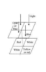
FIGS. 8(a)-8(d) show four preferred embodiments in Bayer patterns for the two-
layer
full spectra color sensing device, respectively, wherein the top layer selects
three or fewer colors
from blank color, blue, green and cyan, while the colors in the bottom layer
are orthogonal to the
colors at the corresponding position in the top layer. In the top layer, same
color pixels are placed
at the diagonal position, thereby forming the generalized Bayer pattern. Many
other patterns are
also possible. Those patterns not only guarantee a full color reconstruction
but also approximately
attain the highest spatial resolution and maximize the use of the incident
light energy. In particular,
the pattern as shown in FIG 8(a) may be used to obtain a sensing device of
CYMK colors, which
has a much larger color representation gamut than the regular CMYK color
sensors, with
independent red and blue colors.
In the present and following embodiments, through strictly following such a
rule that
colors in the bottom layer must be complementary with colors in the top layer,
the maximum use
of the light energy may be achieved. In some embodiments, orthogonal colors
are used instead of
complement colors, and then the spatial resolution may be improved and the
manufacture of the
device may be much simpler.
FIGS. 9(a)-9(d) show four preferred embodiments of two-layer full spectra
color
sensing devices in YUV422 patterns, respectively. Similarly to FIG 8, the same
colors in top layer
are aligned vertically so as to form YUV422 patterns. As shown in FIGS. 9(a)-
9(d), the top layer
comprises up to four colors selected from blank color, blue, green and cyan,
while the colors in
the bottom layer are orthogonal to the colors at the corresponding position in
the top layer,
respectively. Obviously, those skilled in the art can understand, many other
variations are possible
with simple modifications, if required.
FIGS. 10(a)-10(d) show four preferred embodiments of two-layer full spectra
color
sensing devices in honeycomb patterns, respectively. Except that the pixels
are arranged in
honeycomb pattern, the arrangements of pixels in FIGS. 10(a)-10(d) are similar
to that as shown
in FIG 8(a). As honeycomb patterns may have vertical and horizontal
alignments, many
variations can be implemented. The top layer comprises one to three colors
selected from blank
color, blue, green and cyan, while the colors in the bottom layer are
orthogonal to the colors at the
corresponding position in the top layer, respectively.
When the top layer is empty and the bottom layer comprises just sensing pixels
sensing only two spectra, the two-layer sensing device becomes a single layer
sensing device.
That is to say, the present invention includes a single layer sensing device
as a special case of the
12
CA 02705315 2010-01-07
WO 2009/006776
PCT/CN2007/071262
two-layer sensing device, as shown in FIGS. 11(a) and 11(b).
FIGS. 11(a) and 11(b) show two preferred embodiments of the single layer
monochrome multi-spectrum sensing device in which sensing pixels are arranged
in diagonal
patterns, which may be used to sense the visible light and infrared
simultaneously. In this device,
one type of the sensing pixel may be used to sense the visible light (white),
and another type may
be just used to senses infrared, or the full spectrum of the entire visible
light and infrared. The
pattern as shown in FIG 11(a) is applicable to infrared cutting filters, which
can be varied to have
sensing pixels sensing white and infrared (or white + infrared) in YUV422
patterns.
FIGS. 12(a) and 12(b) show preferred embodiments of the two-layer multi-
spectrum
monochrome sensing device and variations thereof, which can sense the visible
light and infrared
simultaneously. FIG 12(a) is in rectangular patterns, FIG 12(b) is in
honeycomb patterns, and
both may sense the visible light and infrared simultaneously. The top layer
senses white light or
transparence, while the bottom layer senses the infrared or full spectrum
(white + infrared).
FIGS. 13(a) and 13(b) show preferred embodiments of the two-layer multi-
spectrum
color sensing device and variations thereof, which can sense the visible light
and infrared
simultaneously. The embodiments can have various structures, and FIGS. 13(a)
and 13(b) are just
two examples. In the figures, sensing pixels sensing infrared are always
disposed in the bottom
layer, which can be either alone or integrated with those sensing another
color (e.g. white +
infrared or red + infrared). The pixels sensing the same color are placed at
the diagonal positions
in order to obtain a higher spatial resolution. Similarly, the top layer
comprises sensing pixels
sensing one to four colors selected from blank color, blue, green and cyan,
while the colors sensed
by sensing pixels in the bottom layer are orthogonal or complementary to those
sensed by sensing
pixels disposed at the corresponding positions in the top layer, respectively.
Another type of two-layer multi-spectrum color sensing device is shown in
FIGS.
14(a) and 14(b), which can sense visible light and infrared simultaneously. In
the device,
infrared is always sensed in the bottom layer, which can be sensed either
alone or together with
another color (e.g. white + infrared or red + infrared). Sensing pixels
sensing the same color are
aligned vertically in order to form YUV422 pattern. Similarly, the top layer
senses from one to
four colors selected from blank color, blue, green and cyan, while colors
sensed by the bottom
layer are orthogonal or complementary to those sensed by pixels disposed at
the corresponding
positions in the top layer.
Another type of two-layer multi-spectrum color sensing device is shown in
FIGS. 15(a)
and 15(b), which adopts honeycomb pattern and may be utilized to sense the
visible light and
infrared simultaneously. In this type of device, infrared is always sensed in
the bottom layer,
13
CA 02705315 2010-01-07
WO 2009/006776
PCT/CN2007/071262
which can be sensed either alone or together with another color (e.g. white +
infrared or red +
infrared). Similarly, the top layer senses from one to three colors selected
from blank color, blue,
green and cyan, while colors sensed in the bottom layer are orthogonal or
complementary to those
sensed by pixels at the corresponding positions in the top layer.
Yet another type of two-layer multi-spectrum color sensing device that
strictly uses
layer lines is shown in FIGS. 16(a) and 16(b). FIG 16(a) adopts a first layer
line and FIG 16(b)
adopts a second layer line. In the embodiments, although white color comprises
a spectral band
above the layer line, white color can be implemented in the bottom layer since
the corresponding
color in the top layer is blank or transparent, as mentioned previously.
Sensing pixels that are
layered strictly according to the layer line (through color filters) have the
advantages that they can
be disposed at the same depth and that a layer can have the same thickness.
There are many
methods for layering sensing pixels according to the layer line.
Hereinafter, referring to FIG. 8(a), is given an example of a method for
manufacturing
the full spectrum color sensing device according to the present invention.
1. A top layer and a bottom layer are provided, respectively. At the top layer
are
disposed sensing pixels sensing a first group of colors: blue, cyan, and blank
color (namely
transparence), and at the bottom layer are disposed sensing pixels sensing a
second group of
colors: yellow, red and white.
2. The sensing pixels are disposed at the bottom layer and top layer such that
the
wavelength of a color sensed in the bottom layer is longer than that of colors
sensed by the
sensing pixels at the corresponding position in the top layer, and the
spectrum of the colors sensed
in the bottom layer is orthogonal or complementary to the total spectrum of
the colors sensed by
the pixels at the corresponding position in the top layer within the spectral
space of visible light.
Specifically, as shown in FIG 8(a), when color sensed in the top layer is
blue, color sensed at the
corresponding position in the bottom layer may be yellow or red; when color
sensed in the top
layer is cyan or blue, color sensed at the corresponding position in the
bottom layer may be red;
when color sensed in the top layer is blank, color sensed at the corresponding
position in the
bottom layer may be any color, but white color can render the incident light
energy maximally
used.
Those skilled in the art may understand that methods for manufacturing full
spectrum
color sensing devices as illustrated in other figures are identical or similar
to the above, which are
not described herein.
Those skilled in the art may also understand that, through varying the
ordering of
pixels in the top layer and bottom layer, various implementations different
from the above
14
CA 02705315 2013-11-27
preferred embodiments will be easily obtained. For example, if needed, those
skilled in the art
' can appreciate that middle layers can also be provided according to
the principle of maximizing
the use of the incident light energy or obtaining the highest spatial
resolution. The wavelength of
each color sensed in a lower layer is required to be longer than that of
colors sensed at the
corresponding position in an upper layer; and the spectrum of each color
sensed in the lower
layer to be orthogonal to the total spectrum of colors at the corresponding
position in all upper
layers within the spectral space of visible light. The spectrum of each color
sensed in the bottom
layer is orthogonal to that of colors sensed at the corresponding position in
all upper layers
within the spectral space of visible light or a combined space of visible
light and infrared.
Preferably, the spectrum of each color sensed in the lower layer should be
complementary to the
total spectrum of colors sensed at the corresponding position in all upper
layers within the
spectral space of visible light.
In conclusion, one feature of the present invention is to make maximum use of
energy of incident light, or to maximize a spatial resolution, or to obtain a
larger color
representation gamut at a low cost, through delicately ordering and
configuring sensing pixels at
a single-, two- or multi-layer in color sensing devices. Although the present
invention is
disclosed through the preferred embodiments, such disclosure should not be
considered
limitations to the invention. For artisan in the image sensing devices (such
as semiconductor
image sensor chips), upon the disclosure, it is possible to anticipate many
variations and
extensions of the present invention. The scope of the claims should not be
limited by the
preferred embodiments set forth in the examples, but should be given the
broadest interpretation
consistent with the description as a whole. As such, various modifications and
additions to the
disclosed apparatus will occur to those skilled in the art, without departing
from the scope of the
claims as purposively construed.