Note: Descriptions are shown in the official language in which they were submitted.
CA 02705332 2012-04-03
ELECTROMAGNETIC RADIATION SHIELDING DEVICE
BACKGROUND OF THE INVENTION
1. Field of the Invention
[0002] This invention relates generally to electromagnetic radiation shielding
panels,
such as windows or insulated glass units (IGU), useful for shielding against
electromagnetic
eavesdropping.
2. Technical Considerations
[0003] Electromagnetic radiation of various frequencies is produced from many
sources, such as computer equipment, radio equipment, communications devices,
telephones, and wireless networks, just to name a few. If this electromagnetic
radiation
were to be intercepted, it could be analyzed and the underlying data obtained.
In order to
prevent such interception, these devices can be kept in protected, e.g.,
shielded, rooms and
great care is be taken to prevent the passage of such radiation outside of the
protected area
in which the equipment is located. This is particularly true in the case of
confidential or
classified information. While building walls typically do an adequate job of
containing this
radiation, conventional building windows are known to permit such radiation to
escape.
[0004] In the past, it has been known to place metallic or polymeric foils
over the
windows to reduce radiation loss. While this does solve the problem of
radiation loss, it
reduces or eliminates the natural sunlight entering the building and prevents
the building
occupants from looking out of the windows. This can have a demoralizing effect
on the
occupants and makes the workplace itself less appealing.
[0005] Solar control coatings are known which affect the transmission of solar
radiation through a window. These solar control coatings are typically highly
transparent to
visible light and are designed to reduce the passage of solar infrared energy
into the building
to prevent heat build-up in the building while still allowing the occupants to
look out through
the window. While these solar control coatings work well to control solar
radiation entering
the building through a window, they have, to date, not been adequate to
prevent the escape
of electromagnetic radiation from computers and other equipment out of the
window.
-1-
CA 02705332 2010-05-10
WO 2009/064742 PCT/US2008/083152
[0006] Therefore, it would be desirable to provide a coating and/or coated
article that
could be used not only to provide solar control properties while maintaining a
desirable
visible light transmission but that also provide electromagnetic shielding
properties.
SUMMARY OF THE INVENTION
[0007] An electromagnetic radiation shielding device comprises a first ply
having a
No. 1 surface and a No. 2 surface and a second ply having a No. 3 surface and
a No. 4
surface. The No. 2 surface of the first ply faces the No. 3 surface of the
second ply. A first
coating having three or more metallic layers is provided over at least a
portion of one of the
surfaces, such as over at least a portion of the No. 1 or No. 2 surface. A
second coating
having three or more metallic layers is provided over at least a portion of
one or more of the
other surfaces, such as over at least a portion of the No. 3 or No. 4 surface.
The first and/or
second coatings have both solar control and electromagnetic shielding
properties.
[0008] In one embodiment, the radiation shielding device is a laminated
article in
which the plies are secured together by a polymeric interlayer. In another
embodiment, the
radiation shielding device is in the form of an IGU, with the spaced plies
held in a spacer
assembly.
[0009] Another electromagnetic radiation shielding device comprises a first
ply
having a No. 1 surface and a No. 2 surface and a second ply spaced from the
first ply and
having a No. 3 surface and a No. 4 surface, with the No. 2 surface facing the
No. 3 surface.
A first coating is formed over at least a portion of the No. 2 surface and
comprises at least
three metallic layers. A second coating is formed over at least a portion of
the No. 3 surface
and comprises at least three metallic layers.
[0010] A method of shielding electromagnetic radiation comprises providing a
first
ply having a No. 1 surface and a No. 2 surface; forming a first coating over
at least a portion
of the No. 2 surface, the first coating comprising at least three metallic
silver layers;
providing a second ply spaced from the first ply and having a No. 3 surface
and a No. 4
surface, with the No. 3 surface forming the No. 2 surface; and forming a
second coating over
at least a portion of the No. 3 surface, the second coating comprising at
least three metallic
silver layers.
BRIEF DESCRIPTION OF THE DRAWINGS
[0011] The invention will be described with reference to the following drawing
figures
wherein like reference numbers identify like parts throughout.
[0012] Fig. 1 is an expanded view (not to scale) of a laminated
electromagnetic
shielding device of the invention;
-2-
CA 02705332 2010-05-10
WO 2009/064742 PCT/US2008/083152
[0013] Fig. 2 is a cross-sectional view (not to scale) of a non-limiting
coating suitable
for the invention; and
[0014] Fig. 3 is a cross-sectional view (not to scale) of another non-limiting
embodiment of the invention.
DESCRIPTION OF THE PREFERRED EMBODIMENTS
[0015] As used herein, spatial or directional terms, such as "left", "right",
"inner",
"outer", "above", "below", and the like, relate to the invention as it is
shown in the drawing
figures. However, it is to be understood that the invention can assume various
alternative
orientations and, accordingly, such terms are not to be considered as
limiting. Further, as
used herein, all numbers expressing dimensions, physical characteristics,
processing
parameters, quantities of ingredients, reaction conditions, and the like, used
in the
specification and claims are to be understood as being modified in all
instances by the term
"about". Accordingly, unless indicated to the contrary, the numerical values
set forth in the
following specification and claims may vary depending upon the desired
properties sought to
be obtained by the present invention. At the very least, and not as an attempt
to limit the
application of the doctrine of equivalents to the scope of the claims, each
numerical value
should at least be construed in light of the number of reported significant
digits and by
applying ordinary rounding techniques. Moreover, all ranges disclosed herein
are to be
understood to encompass the beginning and ending range values and any and all
subranges
subsumed therein. For example, a stated range of "1 to 10" should be
considered to include
any and all subranges between (and inclusive of) the minimum value of 1 and
the maximum
value of 10; that is, all subranges beginning with a minimum value of 1 or
more and ending
with a maximum value of 10 or less, e.g., 1 to 3.3, 4.7 to 7.5, 5.5 to 10, and
the like. Further,
as used herein, the terms "formed over", "deposited over", or "provided over"
mean formed,
deposited, or provided on but not necessarily in direct contact with the
surface. For
example, a coating layer "formed over" a substrate does not preclude the
presence of one or
more other coating layers or films of the same or different composition
located between the
formed coating layer and the substrate. As used herein, the terms "polymer" or
"polymeric"
include oligomers, homopolymers, copolymers, and terpolymers, e.g., polymers
formed from
two or more types of monomers or polymers. The terms "visible region" or
"visible light" refer
to electromagnetic radiation having a wavelength in the range of 380 nm to 760
nm. The
terms "infrared region" or "infrared radiation" refer to electromagnetic
radiation having a
wavelength in the range of greater than 760 nm to 100,000 nm. The terms
"ultraviolet
region" or "ultraviolet radiation" mean electromagnetic energy having a
wavelength in the
range of 300 nm to less than 380 nm. Additionally, all documents, such as but
not limited to
-3-
CA 02705332 2010-05-10
WO 2009/064742 PCT/US2008/083152
issued patents and patent applications, referred to herein are to be
considered to be
"incorporated by reference" in their entirety. The "visible transmission" and
"dominant
wavelength" values are those determined using the conventional methods. Those
skilled in
the art will understand that properties such as visible transmission and
dominant wavelength
can be calculated at an equivalent standard thickness, e.g., 5.5 mm, even
though the actual
thickness of a measured glass sample is different than the standard thickness.
[0016] For purposes of the following discussion, the invention will be
discussed with
reference to use as an electromagnetic radiation shielding device. As used
herein, the term
"electromagnetic shielding device" refers to any transparency, such as but not
limited to
vehicle transparencies or architectural transparencies, providing
electromagnetic radiation
shielding properties. However, it is to be understood that the invention could
be practiced
with transparencies in any desired field, such as but not limited to laminated
or non-
laminated residential and/or commercial windows, insulating glass units,
and/or
transparencies for land, air, space, above water and under water vehicles.
Therefore, it is to
be understood that the specifically disclosed exemplary embodiments are
presented simply
to explain the general concepts of the invention and that the invention is not
limited to these
specific exemplary embodiments. Additionally, while a typical "transparency"
can have
sufficient visible light transmission such that materials can be viewed
through the
transparency, in the practice of the invention the "transparency" need not be
transparent to
visible light but may be translucent or opaque (as described below).
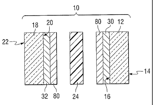
[0017] A non-limiting electromagnetic radiation shielding device 10
incorporating
features of the invention is illustrated in Fig. 1. The device 10 can have any
desired visible
light, infrared radiation, or ultraviolet radiation transmission and
reflection. For example, the
device 10 can have a visible light transmission of any desired amount, e.g.,
greater than 0%
up to 100%. In one non-limiting embodiment, the visible light transmission at
a reference
wavelength of 550 nm can be up to 90%, such as up to 80%, such as up to 70%,
such as up
to 60%, such as up to 50%, such as up to 40%, such as up to 30%, such as up to
20%, such
as in the range of 10% to 99%. In one specific non-limiting embodiment, the
device 10 can
have a visible light transmission of greater than 20%, such as greater than
30%, such as
greater than 40%, such as greater than 50%, such as greater than 60%, such as
greater
than 70%, such as greater than 80%, such as greater than 90%.
[0018] The electromagnetic radiation shielding device 10 includes a first ply
12 with a
first major surface 14, i.e., an outer major surface (No. 1 surface), and an
opposed second
or inner major surface 16 (No. 2 surface). For purpose of discussion, the
first major surface
14 will be considered to face an exterior of a vehicle or building. The
electromagnetic
radiation shielding device 10 also includes a second ply 18 having a first
major surface 20
-4-
CA 02705332 2010-05-10
WO 2009/064742 PCT/US2008/083152
(No. 3 surface) facing the No. 2 surface and a second major surface 22 (No. 4
surface).
This numbering of the ply surfaces is in keeping with conventional practice.
The first ply 12
is spaced from the second ply 18. In the non-limiting embodiment of Fig. 1,
the first and
second plies 12, 18 are spaced apart and bonded together by a conventional
interlayer 24.
Alternatively, as shown in Fig. 3, the first ply 12 and second ply 18 can form
part of a
conventional IGU 100 and can be spaced apart by a conventional spacer assembly
102. A
gap 104 is formed between the plies 12, 18 that can be evacuated or filled
with a selected
gas, such as air or an inert gas.
[0019] As shown in Fig. 1, a first solar control/electromagnetic shielding
coating 30 is
formed over at least a portion of one of the plies 12, 18, such as but not
limited to over at
least a portion of the No. 1 surface 14 or the No. 2 surface 16. A second
solar
control/electromagnetic shielding coating 32 is formed over at least a portion
of one or more
of the other surfaces, such as over at least a portion of the No. 3 surface 20
or the No. 4
surface 22. In the illustrated non-limiting embodiment, the first coating 30
is formed over at
least a portion of the No. 2 surface 16 and the second coating 32 is formed
over at least a
portion of the No. 3 surface 20.
[0020] In the broad practice of the invention, the plies 12, 18 of the device
10 can be
of the same or different materials. The plies 12, 18 can include any desired
material having
any desired characteristics. For example, one or more of the plies 12, 18 can
be transparent
or translucent to visible light. By "transparent" is meant having visible
light transmission of
greater than 0% to 100%. Alternatively, one or more of the plies 12, 18 can be
translucent.
By "translucent" is meant allowing electromagnetic energy (e.g., visible
light) to pass through
but diffusing this energy such that objects on the side opposite the viewer
are not clearly
visible. Examples of suitable materials include, but are not limited to,
plastic substrates
(such as acrylic polymers, such as polyacrylates; polyalkylmethacrylates, such
as
polymethylmethacrylates, polyethylmethacrylates, polypropylmethacrylates, and
the like;
polyurethanes; polycarbonates; polyalkylterephthalates, such as
polyethyleneterephthalate
(PET), polypropyleneterephthalates, polybutyleneterephthalates, and the like;
polysiloxane-
containing polymers; or copolymers of any monomers for preparing these, or any
mixtures
thereof); ceramic substrates; glass substrates; or mixtures or combinations of
any of the
above. For example, one or more of the plies 12, 18 can include conventional
soda-lime-
silicate glass, borosilicate glass, or leaded glass. The glass can be clear
glass. By "clear
glass" is meant non-tinted or non-colored glass. Alternatively, the glass can
be tinted or
otherwise colored glass. The glass can be annealed or heat-treated glass. As
used herein,
the term "heat treated" means tempered or at least partially tempered. The
glass can be of
any type, such as conventional float glass, and can be of any composition
having any optical
properties, e.g., any value of visible transmission, ultraviolet transmission,
infrared
-5-
CA 02705332 2010-05-10
WO 2009/064742 PCT/US2008/083152
transmission, and/or total solar energy transmission. By "float glass" is
meant glass formed
by a conventional float process in which molten glass is deposited onto a
molten metal bath
and controllably cooled to form a float glass ribbon. The first and second
plies 12, 18 can
each be, for example, clear float glass or can be tinted or colored glass or
one ply 12, 18 can
be clear glass and the other ply 12, 18 colored glass. Although not limiting
to the invention,
examples of glass suitable for the first ply 12 and/or second ply 18 are
described in U.S.
Patent Nos. 4,746,347; 4,792,536; 5,030,593; 5,030,594; 5,240,886; 5,385,872;
and
5,393,593. The first and second plies 12, 18 can be of any desired dimensions,
e.g., length,
width, shape, or thickness. In one exemplary embodiment, the first and second
plies can
each be 1 mm to 20 mm thick, such as 1 mm to 15 mm thick, such as 3 mm to 10
mm, such
as 4 mm to 8 mm, such as 6 mm thick.
[0021] In one non-limiting embodiment, one or both of the plies 12, 18 can
have a
high visible light transmission at a reference wavelength of 550 nanometers
(nm). By "high
visible light transmission" is meant visible light transmission at 550 nm of
greater than or
equal to 85%, such as greater than or equal to 87%, such as greater than or
equal to 90%,
such as greater than or equal to 91 %, such as greater than or equal to 92%.
Particularly
useful glass for the practice of the invention is disclosed in U.S. Patent
Nos. 5,030,593
and 5,030,594 and is commercially available from PPG Industries, Inc. under
the mark
Starph i re .
[0022] In another non-limiting embodiment, one ply can comprise a material
having a
higher visible light transmission than the other ply at equal thicknesses. For
example, in one
non-limiting embodiment, the first ply 12 comprises a high visible light
transmission glass of
the type described above and the second ply 18 comprises clear or colored
glass having a
lower visible light transmission than the first ply 12. For example and
without limiting the
present invention, the first ply 12 can have a visible light transmission at
550 nm greater than
or equal to 90%, such as greater than or equal to 91 %, such as greater than
or equal to
92%. The second ply 18 can have a visible light transmission at 550 nm up to
90%, such as
up to 85%, such as up to 80%, such as up to 70%, such as up to 60%, such as up
to 50%,
such as up to 30%, such as up to 20%. Non-limiting examples of glass that can
be used for
the practice of the invention, e.g., for the second ply, include Solargreen ,
Solextra , GL-
208, GL-35TM, Solarbronze , and Solargray glass, all commercially available
from PPG
Industries Inc. of Pittsburgh, Pennsylvania. In one particular non-limiting
embodiment, the
first ply 12 comprises Starphire glass (commercially available from PPG
Industries, Inc.)
having a thickness in the range of 1 mm to 10 mm, such as 1.7 mm to 2.5 mm,
e.g., 2.1 mm
and the second ply comprises GL208 glass having a thickness in the range of 1
mm to 10
mm, such as 1.7 mm to 2.5 mm, e.g., 2.1 mm. In a further non-limiting
embodiment, one or
both of the plies 12, 18 can be annealed glass.
-6-
CA 02705332 2010-05-10
WO 2009/064742 PCT/US2008/083152
[0023] The interlayer 24 can be of any desired material and can include one or
more
layers or plies. The interlayer 24 can be a polymeric or plastic material,
such as, for
example, polyvinylbutyral, plasticized polyvinyl chloride, or multi-layered
thermoplastic
materials including polyethyleneterephthalate, etc. Suitable interlayer
materials are
disclosed, for example but not to be considered as limiting, in U.S. Patent
Nos. 4,287,107
and 3,762,988. The interlayer 24 secures the first and second plies 12, 18
together, can
provide energy absorption, can reduce noise, and can increase the strength of
the laminated
structure. The interlayer 24 can also be a sound-absorbing or attenuating
material as
described, for example, in U.S. Patent No. 5,796,055. The interlayer 24 can
have a solar
control coating provided thereon or incorporated therein or can include a
colored material to
reduce solar energy transmission and/or to provide a color to the device 10.
In one non-
limiting embodiment, the interlayer 24 is polyvinylbutyral and has a thickness
in the range
of 0.5 mm to 1.5 mm, such as 0.75 mm to 0.8 mm.
[0024] The coatings 30 and 32 can be the same or different. The coatings 30,
32
provide the device 10 with both solar control and electromagnetic shielding
properties. By
"solar control" is meant a coating comprised of one or more layers or films
that affect the
solar properties of the coated article, such as but not limited to the amount
of solar radiation,
for example, visible, infrared, or ultraviolet radiation, reflected from,
absorbed by, or passing
through the coated article; shading coefficient; emissivity, etc. A solar
control coating can
block, absorb or filter selected portions of the solar spectrum, such as but
not limited to the
infrared (IR), ultraviolet (UV), and/or visible spectrums. By "electromagnetic
shielding" is
meant a coating that prevents or reduces the passage of electromagnetic
radiation, such as
one or more selected wavelengths of radiation, through the coated article. The
coating can
block, absorb or filter selected portions of the electromagnetic spectrum.
Examples of
coatings that can be used in the practice of the invention are found, for
example but not to
be considered as limiting, in U.S. Patent Nos. 4,898,789; 5,821,001;
4,716,086; 4,610,771;
4,902,580; 4,716,086; 4,806,220; 4,898,790; 4,834,857; 4,948,677; 5,059,295;
and
5,028,759, and also in U.S. Patent Application Serial No. 09/058,440.
[0025] An exemplary coating 30 will now be described. It will be understood
that the
second coating 32 can be the same as the first coating 30. In one non-limiting
embodiment,
the coating 30 can include one or more metallic films positioned between pairs
of dielectric
layers applied sequentially over at least a portion of one of the glass plies
12, 18. The
coating 30 can be a heat and/or radiation reflecting coating and can have one
or more
coating layers or films of the same or different composition and/or
functionality. As used
herein, the term "film" refers to a coating region of a desired or selected
coating composition.
A "layer" can comprise one or more "films" and a "coating" or "coating stack"
can comprise
-7-
CA 02705332 2010-05-10
WO 2009/064742 PCT/US2008/083152
one or more "layers". For example, the coating 30 can be a single layer
coating or a multi-
layer coating and can include one or more metals, non-metals, semi-metals,
semiconductors, and/or alloys, compounds, compositions, combinations, or
blends thereof.
For example, the coating 30 can be a single layer metal oxide coating, a
multiple layer metal
oxide coating, a non-metal oxide coating, a metallic nitride or oxynitride
coating, a non-
metallic nitride or oxynitride coating, or a multiple layer coating comprising
one or more of
any of the above materials. In one non-limiting embodiment, the coating 30 can
be a doped
metal oxide coating.
[0026] The coating 30 can be a functional coating. As used herein, the term
"functional coating" refers to a coating that modifies one or more physical
properties of the
substrate over which it is deposited, e.g., optical, thermal, chemical or
mechanical
properties, and is not intended to be entirely removed from the substrate
during subsequent
processing. The coating 30 can have one or more functional coating layers or
films of the
same or different composition or functionality.
[0027] The coating 30 can also be an electroconductive low emissivity coating
that
allows visible wavelength energy to be transmitted through the coating but
reflects longer
wavelength solar infrared energy. By "low emissivity" is meant emissivity less
than 0.4, such
as less than 0.3, such as less than 0.2, such as less than 0.1, e.g., less
than or equal to
0.05. Examples of low emissivity coatings are found, for example, in U.S.
Patent Nos.
4,952,423 and 4,504,109 and British reference GB 2,302,102.
[0028] Non-limiting examples of suitable coatings 30 for use with the
invention are
commercially available from PPG Industries, Inc. of Pittsburgh, Pennsylvania
under the
SUNGATE and SOLARBAN families of coatings. Such coatings typically include
one or
more anti-reflective coating films comprising dielectric or anti-reflective
materials, such as
metal oxides or oxides of metal alloys, which are transparent to visible
light. The coating 30
can also include one or more infrared reflective films comprising a reflective
metal, e.g., a
noble metal such as gold, copper or silver, or combinations or alloys thereof,
and can further
comprise a primer film or barrier film, such as titanium, as is known in the
art, located over
and/or under the metal reflective layer. The coating 30 can have any desired
number of
infrared reflective films, such as but not limited to 1 to 7 infrared
reflective films. In one non-
limiting embodiment, the coating 30 can have 1 or more silver layers, e.g., 2
or more silver
layers, e.g., 3 or more silver layers, such as 4 or more silver layers, such
as 5 or more silver
layers, such as 6 or more silver layers. The coatings 30, 32 can have the same
or different
number of infrared reflective films and the corresponding infrared reflective
films of the
coatings 30, 32 can have the same or different thicknesses. A non-limiting
example of a
-8-
CA 02705332 2010-05-10
WO 2009/064742 PCT/US2008/083152
suitable coating having three silver layers is disclosed in U.S. Patent
Application Serial No.
10/364,089 (U.S. Publication No. 2003/0180547 Al).
[0029] The coating 30 can be deposited by any conventional method, such as but
not limited to conventional chemical vapor deposition (CVD) and/or physical
vapor
deposition (PVD) methods. Examples of CVD processes include spray pyrolysis.
Examples
of PVD processes include electron beam evaporation and vacuum sputtering (such
as
magnetron sputter vapor deposition (MSVD)). Other coating methods could also
be used,
such as but not limited to sol-gel deposition. In one non-limiting embodiment,
the coating 30
can be deposited by MSVD. Examples of MSVD coating devices and methods will be
well
understood by one of ordinary skill in the art and are described, for example,
in U.S. Patent
Nos. 4,379,040; 4,861,669; 4,898,789; 4,898,790; 4,900,633; 4,920,006;
4,938,857;
5,328,768; and 5,492,750.
[0030] An exemplary non-limiting coating 30 suitable for the invention is
shown in
Fig. 2. This exemplary coating 30 includes a base layer or first dielectric
layer 40 deposited
over at least a portion of a major surface of a substrate (e.g., the No. 2
surface 16 of the first
ply 12). The first dielectric layer 40 can comprise one or more films of anti-
reflective
materials and/or dielectric materials, such as but not limited to metal
oxides, oxides of metal
alloys, nitrides, oxynitrides, or mixtures thereof. The first dielectric layer
40 can be
transparent to visible light. Examples of suitable metal oxides for the first
dielectric layer 40
include oxides of titanium, hafnium, zirconium, niobium, zinc, bismuth, lead,
indium, tin, and
mixtures thereof. These metal oxides can have small amounts of other
materials, such as
manganese in bismuth oxide, tin in indium oxide, etc. Additionally, oxides of
metal alloys or
metal mixtures can be used, such as oxides containing zinc and tin (e.g., zinc
stannate),
oxides of indium-tin alloys, silicon nitrides, silicon aluminum nitrides, or
aluminum nitrides.
Further, doped metal oxides, such as antimony or indium doped tin oxides or
nickel or boron
doped silicon oxides, can be used. The first dielectric layer 40 can be a
substantially single
phase film, such as a metal alloy oxide film, e.g., zinc stannate, or can be a
mixture of
phases composed of zinc and tin oxides or can be composed of a plurality of
metal oxide
films, such as those disclosed in U.S. Patent Nos. 5,821,001; 4,898,789; and
4,898,790.
[0031] In the illustrated exemplary embodiment shown in Fig. 2, the first
dielectric
layer 40 can comprise a multi-film structure having a first film 42, e.g., a
metal alloy oxide
film, deposited over at least a portion of the inner major surface 16 of the
first ply 12 and a
second film 44, e.g., a metal oxide or oxide mixture film, deposited over the
first metal alloy
oxide film 42. In one non-limiting embodiment, the first film 42 can be a
zinc/tin alloy oxide.
The zinc/tin alloy oxide can be that obtained from magnetron sputtering vacuum
deposition
from a cathode of zinc and tin that can comprise zinc and tin in proportions
of 10 wt.% to 90
-9-
CA 02705332 2010-05-10
WO 2009/064742 PCT/US2008/083152
wt.% zinc and 90 wt.% to 10 wt.% tin. One suitable metal alloy oxide that can
be present in
the first film 42 is zinc stannate. By "zinc stannate" is meant a composition
of ZnxSnl-x02-x
(Formula 1) where "x" varies in the range of greater than 0 to less than 1.
For instance, "x"
can be greater than 0 and can be any fraction or decimal between greater than
0 to less than
1. For example where x = 2/3, Formula 1 is Zn213Sn13O413, which is more
commonly
described as "Zn2SnO4". A zinc stannate-containing film has one or more of the
forms of
Formula 1 in a predominant amount in the film. In one non-limiting embodiment,
the first film
42 comprises zinc stannate and has a thickness in the range of 100 A to 500 A,
such as 150
A to 400 A, e.g., 200 A to 300 A, e.g., 260 A.
[0032] The second film 44 can be a zinc-containing film, such as zinc oxide.
The
zinc oxide film can be deposited from a zinc cathode that includes other
materials to improve
the sputtering characteristics of the cathode. For example, the zinc cathode
can include a
small amount (e.g., less than 10 wt.%, such as greater than 0 to 5 wt.%) of a
conductive
material, such as tin, to improve sputtering. In which case, the resultant
zinc oxide film
would include a small percentage of tin oxide, e.g., 0 to less than 10 wt.%
tin oxide, e.g., 0 to
wt.% tin oxide. An oxide layer sputtered from a zinc/tin cathode having ninety-
five percent
zinc and five percent tin is still referred to herein as a zinc oxide film.
The small amount of
tin in the cathode (e.g., less than 10 wt.%) is believed to form a small
amount of tin oxide in
the predominantly zinc oxide-containing second film 44. The second film 44 can
have a
thickness in the range of 50 A to 200 A, such as 75 A to 150 A, e.g., 100 A.
In one non-
limiting embodiment in which the first film 42 is zinc stannate and the second
film 44 is zinc
oxide, the first dielectric layer 40 can have a total thickness of less than
or equal to 1,000 A,
such as less than or equal to 500 A, e.g., 300 A to 450 A, e.g., 350 A to 425
A, e.g., 400 A.
[0033] A first heat and/or radiation reflective film or layer 46 can be
deposited over
the first dielectric layer 40. The first reflective layer 46 can include a
reflective metal, such
as but not limited to metallic gold, copper, silver, or mixtures, alloys, or
combinations thereof.
In one embodiment, the first reflective layer 46 comprises a metallic silver
layer having a
thickness in the range of 25 A to 300 A, e.g., 50 A to 300 A, e.g., 50 A to
200 A, such as 70
A to 150 A, such as 100 A to 150 A, e.g., 130 A.
[0034] A first primer film 48 can be deposited over the first reflective layer
46. The
first primer film 48 can be an oxygen-capturing material, such as titanium,
that can be
sacrificial during the deposition process to prevent degradation or oxidation
of the first
reflective layer 46 during the sputtering process or subsequent heating
processes. The
oxygen-capturing material can be chosen to oxidize before the material of the
first reflective
layer 46. If titanium is used as the first primer film 48, the titanium would
preferentially
oxidize to titanium dioxide during subsequent processing of the coating before
oxidation of
-10-
CA 02705332 2010-05-10
WO 2009/064742 PCT/US2008/083152
the underlying silver layer. In one embodiment, the first primer film 48 is
titanium having a
thickness in the range of 5 A to 50 A, e.g., 10 A to 40 A, e.g., 15 A to 25 A,
e.g., 20 A.
[0035] An optional second dielectric layer 50 can be deposited over the first
reflective layer 46 (e.g., over the first primer film 48). The second
dielectric layer 50 can
comprise one or more metal oxide or metal alloy oxide-containing films, such
as those
described above with respect to the first dielectric layer. In the illustrated
non-limiting
embodiment, the second dielectric layer 50 includes a first metal oxide film
52, e.g., a zinc
oxide film deposited over the first primer film 48. A second metal alloy oxide
film 54, e.g., a
zinc stannate (Zn2SnO4) film, can be deposited over the first zinc oxide film
52. A third metal
oxide film 56, e.g., another zinc/tin oxide layer, can be deposited over the
zinc stannate layer
to form a multi-film second dielectric layer 50. In one non-limiting
embodiment, the zinc
oxide films 52, 56 of the second dielectric layer 50 can each have a thickness
in the range of
about 50 A to 200 A, e.g., 75 A to 150 A, e.g., 100 A. The metal alloy oxide
layer (zinc
stannate) 54 can have a thickness in the range of 100 A to 800 A, e.g., 200 A
to 700 A, e.g.,
300 A to 600 A, e.g., 550 A to 600 A.
[0036] An optional second heat and/or radiation reflective layer 58 can be
deposited
over the second dielectric layer 50. The second reflective layer 58 can
include any one or
more of the reflective materials described above with respect to the first
reflective layer 46.
In one non-limiting embodiment, the second reflective layer 58 comprises
silver having a
thickness in the range of 25 A to 200 A, e.g., 50 A to 150 A, e.g., 80 A to
150 A, e.g., 100 A
to 150 A, e.g., 130 A. In another non-limiting embodiment, this second
reflective layer 58
can be thicker than the first and/or third reflective layers (the third
reflective layer to be
discussed later).
[0037] An optional second primer film 60 can be deposited over the second
reflective
layer 58. The second primer film 60 can be any of the materials described
above with
respect to the first primer film 48. In one non-limiting embodiment, the
second primer film
includes titanium having a thickness in the range of about 5 A to 50 A, e.g.,
10 A to 25 A,
e.g., 15 A to 25 A, e.g., 20 A.
[0038] An optional third dielectric layer 62 can be deposited over the second
reflective layer 58 (e.g., over the second primer film 60). The third
dielectric layer 62 can
also include one or more metal oxide or metal alloy oxide-containing layers,
such as
discussed above with respect to the first and second dielectric layers 40, 50.
In one non-
limiting embodiment, the third dielectric layer 62 is a multi-film layer
similar to the second
dielectric layer 50. For example, the third dielectric layer 62 can include a
first metal oxide
layer 64, e.g., a zinc oxide layer, a second metal alloy oxide-containing
layer 66, e.g., a zinc
stannate layer (Zn2SnO4), deposited over the zinc oxide layer 64, and a third
metal oxide
-11-
CA 02705332 2010-05-10
WO 2009/064742 PCT/US2008/083152
layer 68, e.g., another zinc oxide layer, deposited over the zinc stannate
layer 66. In one
non-limiting embodiment, the zinc oxide layers 64, 68 can have thicknesses in
the range of
50 A to 200 A, such as 75 A to 150 A, e.g., 100 A. The metal alloy oxide layer
66 can have
a thickness in the range of 100 A to 800 A, e.g., 200 A to 700 A, e.g., 300 A
to 600 A, e.g.,
550 A to 600 A.
[0039] In one non-limiting aspect of the invention, the second dielectric
layer 50 and
third dielectric layer 62 have thicknesses that are within 10% of each other,
such as within
5%, such as within 3% of each other, such as within 2% of each other.
[0040] The coating 30 can further include an optional third heat and/or
radiation
reflective layer 70 deposited over the third dielectric layer 62. The third
reflective layer 70
can be of any of the materials discussed above with respect to the first and
second reflective
layers. In one non-limiting embodiment, the third reflective layer 70 includes
silver and has a
thickness in the range of 25 A to 300 A, e.g., 50 A to 300 A, e.g., 50 A to
200 A, such as 70
A to 150 A, such as 100 A to 150 A, e.g., 120 A. In one non-limiting aspect of
the invention,
the first reflective layer 46 and third reflective layer 70 have thicknesses
that are within 10%
of each other, such as within 5%, of each other, such as within 3% of each
other, such as
within 2% of each other.
[0041] An optional third primer film 72 can be deposited over the third
reflective layer
70. The third primer film 72 can be of any of the primer materials described
above with
respect to the first or second primer films. In one non-limiting embodiment,
the third primer
film is titanium and has a thickness in the range of 5 A to 50 A, e.g., 10 A
to 25 A, e.g., 20 A.
[0042] An optional fourth dielectric layer 74 can be deposited over the third
reflective
layer (e.g., over the third primer film 72). The fourth dielectric layer 74
can be comprised of
one or more metal oxide or metal alloy oxide-containing layers, such as those
discussed
above with respect to the first, second, or third dielectric layers 40, 50,
62. In one non-
limiting embodiment, the fourth dielectric layer 74 is a multi-film layer
having a first metal
oxide layer 76, e.g., a zinc oxide layer, deposited over the third primer film
72, and a second
metal alloy oxide layer 78, e.g., a zinc stannate layer (Zn2SnO4), deposited
over the zinc
oxide layer 76. The zinc oxide layer 76 can have a thickness in the range of
25 A to 200 A,
such as 50 A to 150 A, such as 100 A. The zinc stannate layer 78 can have a
thickness in
the range of 25 A to 500 A, e.g., 50 A to 500 A, e.g., 100 A to 400 A, e.g.,
200 A to 300 A,
e.g., 260 A.
[0043] The coating 30 can contain any number of additional groups of
dielectric
layer/reflective metal layer/primer layer units as desired. In one particular
non-limiting
embodiment, the coating 30 can contain up to six anti-reflective metal layers,
e.g., up to six
silver layers, along with the associated dielectric layers.
-12-
CA 02705332 2010-05-10
WO 2009/064742 PCT/US2008/083152
[0044] The coating 30 can include a protective overcoat 80, which, for example
in
the non-limiting embodiment shown in Fig. 2, is deposited over the optional
fourth dielectric
layer 74 (if present), to assist in protecting the underlying layers, such as
the anti-reflective
layers, from mechanical and chemical attack during processing. The protective
coating 80
can be an oxygen barrier coating layer to prevent or reduce the passage of
ambient oxygen
into the underlying layers of the coating 30 during subsequent processing,
e.g., such as
during heating or bending. The protective coating 80 can be of any desired
material or
mixture of materials. In one exemplary embodiment, the protective coating 80
can include a
layer having one or more metal oxide materials, such as but not limited to
oxides of
aluminum, silicon, or mixtures thereof.
[0045] The protective coating 80 can be of any desired thickness. In one
exemplary
laminated article embodiment, the protective coating 80 can have a thickness
in the range of
100 A to 50,000 A, such as 500 A to 50,000 A, e.g., 500 A to 10,000 A, such as
100 A to
2,000 A. Further, the protective coating 80 can be of non-uniform thickness.
By "non-
uniform thickness" is meant that the thickness of the protective coating 80
can vary over a
given unit area, e.g., the protective coating 80 can have high and low spots
or areas.
[0046] The protective coating 80 can be of any desired material or mixture of
materials. In one exemplary embodiment, the protective coating 80 can include
one or more
metal oxide materials, such as but not limited to, aluminum oxide, silicon
oxide, or mixtures
thereof. For example, the protective coating 80 can be a single coating layer
comprising in
the range of 0 wt.% to 100 wt.% alumina and/or 0 wt.% to 100 wt.% silica, such
as 5 wt.% to
100 wt.% alumina and 95 wt.% to 0 wt.% silica, such as 5 wt.% to 90 wt.%
alumina and 95
wt.% to 10 wt.% silica, such as 10 wt.% to 90 wt.% alumina and 90 wt.% to 10
wt.% silica,
such as 15 wt.% to 90 wt.% alumina and 85 wt.% to 10 wt.% silica, such as 50
wt.% to 70
wt.% alumina and 50 wt.% to 30 wt.% silica, such as 35 wt.% to 100 wt.%
alumina and 65
wt.% to 0 wt.% silica, e.g., 70 wt.% to 90 wt.% alumina and 10 wt.% to 30 wt.%
silica, e.g.,
75 wt.% to 85 wt.% alumina and 15 wt.% to 25 wt.% of silica, e.g., 88 wt.%
alumina and 12
wt.% silica, e.g., 65 wt.% to 75 wt.% alumina and 25 wt.% to 35 wt.% silica,
e.g., 70 wt.%
alumina and 30 wt.% silica. Other materials, such as aluminum, chromium,
hafnium, yttrium,
nickel, boron, phosphorous, titanium, zirconium, and/or oxides thereof, can
also be present.
[0047] Alternatively, the protective coating 80 can be a multilayer coating
formed by
separately formed layers of metal oxide materials, such as but not limited to
a bilayer formed
by one metal oxide containing layer (e.g., an alumina layer or a silica and
alumina containing
first layer) and another metal oxide containing layer (e.g., a silica layer or
a silica and
alumina containing second layer). The individual layers of the multilayer
protective coating
80 can be of any desired thickness.
-13-
CA 02705332 2010-05-10
WO 2009/064742 PCT/US2008/083152
[0048] In one embodiment, the protective coating 80 can comprise a first layer
and a
second layer formed over the first layer. In one non-limiting embodiment, the
first layer can
comprise alumina, or a mixture or alloy comprising alumina and silica. For
example, the first
layer can comprise a silica/alumina mixture having at least 5 wt.% alumina,
such as at least
wt.% alumina, such as at least 15 wt.% alumina, such as at least 30 wt.%
alumina, such
as at least 40 wt.% alumina, such as at least 60 wt.% alumina, such as at
least 70 wt.%
alumina, such as at least 80 wt.% alumina, such as at least 90 wt.% alumina,
such as at
least 95 wt.% alumina, such as 50 wt.% to 70 wt.% alumina, such as in the
range of 70 wt.%
to 100 wt.% alumina and 30 wt.% to 0 wt.% silica, such as in the range of 60
wt.% to 100
wt.% alumina and 40 wt.% to 0 wt.% silica. In one non-limiting embodiment, the
first layer
can have a thickness in the range of greater than 0 A to 1 micron, such as 50
A to 100 A,
such as 100 A to 250 A, such as 100 A to 200 A, such as 100 A to 150 A, such
as greater
than 100 A to 125 A.
[0049] The second layer can comprise silica, or a mixture or alloy comprising
silica
and alumina. For example, the second layer can comprise a silica/alumina
mixture having at
least 40 wt.% silica, such as at least 50 wt.% silica, such as at least 60
wt.% silica, such as
at least 70 wt.% silica, such as at least 80 wt.% silica, such as at least 85
wt.% silica, such
as at least 90 wt.% silica, such as at least 95 wt.% silica, such as in the
range of 80 wt.% to
90 wt.% silica and 10 wt.% to 20 wt.% alumina, e.g., 85 wt.% silica and 15
wt.% alumina. In
one non-limiting embodiment, the second layer can have a thickness in the
range of greater
than 0 A to 2 microns, such as 50 A to 5,000 A, such as 50 A to 2,000 A, such
as 100 A to
1,000 A, such as 300 A to 500 A, such as 350 A to 400 A.
[0050] The second coating 32 can be the same as or substantially the same as
the
first coating 30 described above.
[0051] It is estimated that the above described laminated device 10 would
transmit
less than 1% of the infrared radiation between 800 nm and 2,300 nm. It is also
estimated
that radio frequency attenuation would be at least 20 dB between 800 MHz and 3
GHz. It is
further estimated that the radio frequency attenuation would be at least 20 dB
over the 50
MHz to 20 GHz range.
[0052] It will be readily appreciated by those skilled in the art that
modifications may
be made to the invention without departing from the concepts disclosed in the
foregoing
description. Moreover, as will be appreciated by one of ordinary skill in the
art, the preferred
parameters described above can be adjusted, if required, for different
substrate materials
and/or thicknesses. Accordingly, the particular embodiments described in
detail herein are
illustrative only and are not limiting to the scope of the invention, which is
to be given the full
breadth of the appended claims and any and all equivalents thereof.
-14-