Note: Descriptions are shown in the official language in which they were submitted.
CA 02705553 2010-05-11
WO 2009/064816 PCT/US2008/083283
PROCESSES FOR RAPID MICROFABRICATION USING THERMOPLASTICS
AND DEVICES THEREOF
CROSS REFERENCE TO RELATED APPLICATIONS
The present application claims the benefit under 35 U.S.C. 119(e) of U.S.
Provisional
Serial No. 61/003,113, filed November 13, 2007 and U.S. Provisional Serial No.
61/018,881, filed January 3, 2008, the contents of each of which are hereby
incorporated by
reference into the present disclosure.
FIELD OF THE INVENTION
The invention disclosed herein related to the field of microfabrication.
BACKGROUND OF THE INVENTION
Throughout this disclosure, various technical and patent publications are
referenced to more
fully describe the state of the art to which this invention pertains. These
publications are
incorporated by reference, in their entirety, into this application.
Methods have been developed as lower-cost alternatives to photolithography,
the `gold
standard' for microfabrication and microfluidic device creation. Duffy et al.
first introduced
`rapid prototyping of masters' whereby they used printed transparencies to
replace the
expensive chrome masks traditionally utilized in photolithography (Duffy D.,
et al. (1998)
Anal Chem. 70: 4974-4984). The authors demonstrated the advantages of using
rapid
prototyping for masks over conventional photolithography and micromachining.
Despite its
convenience, the method still requires the use of expensive photoresist, high-
resolution
printing, and contact lithography. Tan et al. obviated this issue by direct
printing; they
photocopied designs onto transparencies to fabricate microfluidic channel
molds that ranged
in height from 8-14 micrometer, depending on the darkness setting of the
photocopy
machine (Tan A., et al. (2001) Lab Chip 1: 7-9). Liu et al. developed a one-
step direct-
printing technique for the design and fabrication of passive micro-mixers in
microfluidic
devices, with a maximum channel height of 11 micrometer (Liu A., et al. (2005)
Lab Chip
5: 974-978). Such shallow channels are adequate for many microfluidic
applications but
not amenable for use with large mammalian cells (>10 micrometer in diameter)
as well as
CA 02705553 2010-05-11
WO 2009/064816 PCT/US2008/083283
other applications, such as flowing chemotactic gradients across adherent
cells in a channel
with minimal shearing (Lin F., et al. (2004) Biochem. And Biophys. Res.
Commun. 319:
576-581).
While Lago et at. introduced a way to circumvent the height limitation of
single-layer ink
by printing up to four times using a thermal toner transfer method onto a
glass substrate, the
maximum height obtained with this approach was 25 micrometer (Lago C.L., et
al. (2004)
Electrophoresis 25: 3825-3831). Vullev et al. demonstrated a non-lithographic
fabrication
approach of microfluidic devices by printing positive-relief masters with a
laser jet printer
for detecting bacterial spores; the height of the channels, which is likewise
dependent on the
height of the ink, is limited to between 5-9 micrometer (Vullev V., et al.
(2006) J. Am.
Chem. Soc. 128: 16062-16072). To achieve deep channels, McDonald et al.
introduced the
use of solid object printing (SOP) to make PDMS molds in thermoplastics
(McDonald J.C.,
et al. (2002) Anal. Chem. 74: 1537-1545). However, despite their versatility,
solid object
printers are considerably costly ($50,000).
Furthermore, the majority of these methods (as well as conventional
photolithography)
produce rectangular cross section channels. Pneumatic valves, first introduced
by Quake et
al., important for many microfluidic applications, require microfluidic
channels to be
rounded such that they can be completely sealed upon valve closure (Unger
M.A., et al.
(2000) Science 288(5463): 113-116). Achieving rounded microfluidic channels
using
typical photolithographic techniques, however, is complicated and requires an
extra re-flow
step of the photoresist at high temperatures. Most recently, Chao et al.
demonstrated an
elegant rapid prototyping approach, coined microscale plasma templating (
PLAT), using
water molds. This technique enables the creation of rounded channels that are
difficult to
make with photolithography, but still requires micromachined masks and plasma
activation
(Chao S.H., et al. (2007) Lab Chip Technical Note 7: 641-643).
SUMMARY OF THE INVENTION
A method is provided to prepare a one or more or a plurality microfluidic
channels on a
receptive material, comprising the steps of a) applying an image-forming
material to a heat
sensitive thermoplastic receptive material, also referred to as thermoplastic
material, in a
2
CA 02705553 2010-05-11
WO 2009/064816 PCT/US2008/083283
designed pattern, b) heating said material under conditions that reduce the
size of the
thermoplastic receptive material, also referred to as thermoplastic material,
material by at
least about 60%, and c) preparing the microfluidic channels via lithography.
In an
alternative aspect, the microfluidic channels are created by lithography on
the image-
formed, heat-reduced thermoplastic material.
Also provided herein is a method to prepare one or more or a plurality of
microfluidic
channels on a receptive material by etching a designed pattern into a heat
sensitive
thermoplastic material support and then heating the material under conditions
that reduce
the size of the thermoplastic receptive material, also referred to as
thermoplastic material,
material by at least about 60%.
The receptive materials prepared by this method are further provided for the
fabrication of
various devices to be used in applications such as biological and chemical
processing and
analysis, micro-mixers, which are necessary for biochemical reactions,
chemical synthesis,
and biological processes such as biochemical detection involving hybridization
analyses,
immunoassays, and cell-molecule interactions, near-field optical microscopy,
sub-
wavelength photonics, biochemical sensing, molecular detection, optical
devices, filters and
sorters, high-surface area conductors and actuators and solar energy
harvesting. Methods of
using such devices are also provided herein.
BRIEF DESCRIPTION OF THE DRAWINGS
Figure 1, panels A and B, show thermoplastic (Shrinky-Dink) mold generation
having a
single microfluidic channel. A) Unshrunken thermoplastic (Shrinky-Dink) master
with
laser printed master pattern. B) The same master after being baked. Masters
shrink from
about 800 micrometers to about 300 micrometers in width. The original height
of the ink
(as measured on transparencies instead of unshrunk thermoplastic because the
thermoplastic
heats up and shrinks when prepped for the SEM) was approximately 10
micrometers but
was difficult to measure precisely on the SEM (see Figure 3B). Insets: SEM of
channel top
view and cross-section through a shrunken channel, illustrating a height of 80
micrometers.
Heights varied depending on the printer used. For this 80 micrometer channel,
the
3
CA 02705553 2010-05-11
WO 2009/064816 PCT/US2008/083283
thermoplastic was double printed with transparency mode on the Hewlett-Packard
LaserJet
2200D.
Figure 2, panels A to D, show process flow. A) The master pattern is produced
using CAD
software and printed directly onto the Shrinky Dink. After baking, the pattern
shrinks by
62.5%. B) PDMS is poured over the master. C) After curing, the PDMS is peeled
off,
containing a negative copy of the master pattern. D) The molded PDMS is bonded
to a
glass slide to form microchannels and the finished microdevice.
Figure 3, panels A and B, show scanning electron micrographs (SEM) of channels
made
from our approach (A) compared to those made using transparencies (B). A)
Perspective
SEM of channel made using a thermoplastic (Shrinky-Dink) mold versus B)
transparency.
The difference in height and shape is apparent.
Figure 4, panels A and B, show functional devices. A) Bonded PDMS gradient
generator
with food dye. B) Bright field image of Chinese Hamster Ovary (CHO) cells
flowing
through a single microfluidic channel.
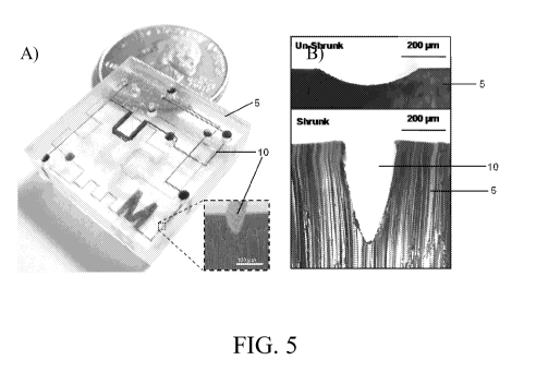
Figure 5, panels A and B, show a thermoplastic (Shrinky-Dink) microchips. (A)
3D micro-
mixers from a thermoplastic (Shrinky-Dink). This is a 3 layer device in which
the blue and
yellow are on different levels and mix to form green on the 3rd layer. (B)
SEMs of various
channel shapes and sizes attained by simply scribing and then heating.
Figure 6, panels A thru D, show images of the metal deposited on the
thermoplastic
material.
Figure 7, panels A thru D, is a schematic of the process for monodirectional
shrinkage of
the thermoplastic material.
Figure 8A is a schematic of nano-wrinkles fabrication. Figure 8B shows SEM
images of
bi-axial (left), uni-axial (middle) and micropatterned (right) wrinkles.
Figure 9 shows a schematic of nano-wrinkles fabrication and SEM images of uni-
axial
(anisotropic, top) and bi-axial (isotropic, bottom) wrinkles.
4
CA 02705553 2010-05-11
WO 2009/064816 PCT/US2008/083283
Figure 10A shows the fabrication of a micro-mixer. Figure lOB shows the final
vortex
micro-mixer versus the 2D serpentine design (Figure 10C). The insets show the
fluorescence overlaid bright field images which illustrate the mixing dynamics
of each
approach.
Figure 11 shows a graph which quantifies the mixing effectiveness as a
function of
Reynolds Number (Re) for both the vortex micro-mixer and the serpentine mixer.
The error
bars represent the standard error of the mean.
Figure 12A shows a graph of bead redistribution using a smaller microvortex
mixer. The
dimensions are illustrated in Figure 12B. Figure 12C shows a 5x5 array of
micro-mixers
integrated into gradient generators.
Figure 13 shows a schematic of the method for forming the metal wrinkles and
SEM
images during different points in the process.
Figure 14A shows the visible absorption spectra indicating absorption at 561
nanometers
for the 30 nanometer thick wrinkles (top line) but no absorption for the flat
(unwrinkled)
control (bottom line). Figure 14B shows a quantum Stark effect as a red shift
of the
quantum-dot (QD) emission.
Figure 15 shows a two dimensional map of the photo-luminescence of a 10 by 10
micron
sample area of a wrinkled metal surface with a thin layer of quantum dots spun
coated on
top. The numbered areas shown displays more of a red shift.
Figure 16 shows a graph correlating the number of prints of the image-forming
material on
the thermoplastic material versus the thickness of the channels produced.
Figure 17 shows a plot of the maximum average wrinkle wavelength as a function
of metal
layer thickness. Wrinkle wavelength control by changing the metal film
thickness.
5
CA 02705553 2010-05-11
WO 2009/064816 PCT/US2008/083283
DETAILED DESCRIPTION OF THE INVENTION
As used herein, certain terms may have the following defined meanings.
As used in the specification and claims, the singular form "a," "an" and "the"
include plural
references unless the context clearly dictates otherwise. For example, the
term "a
microfluidic channel" includes a plurality of microfluidic channels.
As used herein, the term "comprising" is intended to mean that the
compositions and
methods include the recited elements, but do not exclude others. "Consisting
essentially of
when used to define compositions and methods, shall mean excluding other
elements of any
essential significance to the combination when used for the intended purpose.
Thus, a
composition consisting essentially of the elements as defined herein would not
exclude trace
contaminants or inert carriers. "Consisting of shall mean excluding more than
trace
elements of other ingredients and substantial method steps for preparing the
microfluidic
device. Embodiments defined by each of these transition terms are within the
scope of this
invention.
A "thermoplastic material" is intended to mean a plastic material which
shrinks upon
heating. In one aspect, the thermoplastic materials are those which shrink
uniformly
without distortion. A "Shrinky-Dink" is a commercial thermoplastic which is
used a
childrens toy. The shrinking can be either bi-axially (isotropic) or uni-axial
(anisotropic).
Suitable thermoplastic materials for inclusion in the methods of this
invention include, for
example, high molecular weight polymers such as acrylonitrile butadiene
styrene (ABS),
acrylic, celluloid, cellulose acetate, ethylene-vinyl acetate (EVA), ethylene
vinyl alcohol
(EVAL), fluoroplastics (PTFEs, including FEP, PFA, CTFE, ECTFE, ETFE),
ionomers
kydex, a trademarked acrylic/PVC alloy, liquid crystal polymer (LCP),
polyacetal (POM or
Acetal), polyacrylates (Acrylic), polyacrylonitrile (PAN or Acrylonitrile),
polyamide (PA or
Nylon), polyamide-imide (PAI), polyaryletherketone (PAEK or Ketone),
polybutadiene
(PBD), polybutylene (PB), polybutylene terephthalate (PBT), polyethylene
terephthalate
(PET), Polycyclohexylene Dimethylene Terephthalate (PCT), polycarbonate (PC),
polyhydroxyalkanoates (PHAs), polyketone (PK), polyester polyethylene (PE),
polyetheretherketone (PEEK), polyetherimide (PEI), polyethersulfone (PES),
polysulfone
polyethylenechlorinates (PEC), polyimide (PI), polylactic acid (PLA),
polymethylpentene
6
CA 02705553 2010-05-11
WO 2009/064816 PCT/US2008/083283
(PMP), polyphenylene oxide (PPO), polyphenylene sulfide (PPS), polyphthalamide
(PPA),
polypropylene (PP), polystyrene (PS), polysulfone (PSU), polyvinyl chloride
(PVC),
polyvinylidene chloride (PVDC) and spectralon. A "Shrinky-Dink" is a
commercial
thermoplastic material which is marketed as a children's toy. As used herein,
the terms
"thermoplastic base" and "thermoplastic cover" refer to thermoplastic material
having been
subjected to both the etching process as well as heating process. The
"thermoplastic base"
would be located at the bottom or within the device, and the "thermoplastic
cover" is the
last layer of one or more layers of thermoplastic base.
A "channel" is intended to mean a flow path which is disposed within one or
more levels of
the microfluidic network structure. The term "microfluidic" is generally
defined as a
substrate or material having a passage through which a fluid, solid or gas can
pass with at
least one internal cross-sectional dimension that is less than about 500
micrometers and
typically between about 0.1 micrometers and about 500 micrometers which can be
used in
any number of chemical processes involving very small amounts of material
fluid. Such
processes include, but are not limited to, electrophoresis (e.g., capillary
electrophoresis or
CE), chromatography (e.g., liquid chromatography), screening and diagnostics
(using, e.g.,
hybridization or other binding means), and chemical and biochemical synthesis
(e.g., DNA
amplification as may be conducted using the polymerase chain reaction, or
VCR") and
analysis (e.g., through enzymatic digestion).
In addition to the above uses, the microfluidic channels disclosed herein can
be patterned
for "microfluidic mixing." As used herein, the term "microfluidic mixing" is
intended to
mean the use of a receptive material having at least two inlet channels,
wherein the inlet
channels meet or intersect at an overlap region that may be in fluid
communication with an
outlet channel, such that fluids, such as solutions or other material,
introduced from the inlet
channels are mixed and may proceed into an outlet channel.
A "solution" is intended to refer to a substantially homogeneous mixture of a
solute, such as
a solid, liquid, or gaseous substance, with a solvent, which is typically a
liquid. The
solution can be either aqueous or non-aqueous. Examples of suitable solutes in
solutions
include fluorescent dyes, biological compounds, such as proteins, DNA and
plasma, and
soluble chemical compounds. Examples of suitable solids include beads, such as
7
CA 02705553 2010-05-11
WO 2009/064816 PCT/US2008/083283
polystyrene beads, and powders, such as a metal powder. A "suspension" is
intended to
refer to a substantially heterogeneous fluid containing a solid, wherein the
solid is dispersed
throughout the liquid, but does not substantially dissolve. The solid
particles in a
suspension will typically settle as the particle size is large, compared to a
colloid, where the
particle size is small such that the suspension does not settle. Examples of
suitable
suspensions include biological suspensions such as whole blood, cell
compositions, or other
cell containing mixtures. It is contemplated that any solution, solid or
suspension can be
mixed using the mixers disclosed herein, provided that the solid has a
particle size
sufficiently small to move throughout the channels in the mixer.
In general, the image-forming material is one which is compressed upon
heating, bonds to
the plastic and is durable (can be used as a mold for multiple iterations).
For example,
"image-forming material" is, in one aspect, intended to mean a composition,
typically a
liquid, containing various pigments and/or dyes used for coloring a surface to
produce an
image or text such as ink and printer toner. In addition to an ink, the image
forming
material can be a metal, such as gold, titanium, silver, a protein, a colloid,
a dielectric
substance, a paste or any other suitable metal or combination thereof.
Examples of suitable
proteins include biotin, fibronectin and collagen. Examples of suitable
colloids include
pigmented ink, paints and other systems involving small particles of one
substance
suspended in another. Examples of suitable dielectric substances include metal
oxides, such
as aluminum oxide, titanium dioxide and silicon dioxide. Examples of suitable
pastes
include conductive pastes such as silver pastes.
The image forming material can be applied to the thermoplastic material by a
variety of
methods known to one skilled in the art, such as printing, sputtering and
evaporating. The
term "evaporating" is intended to mean thermal evaporation, which is a
physical vapor
deposition method to deposit a thin film of metal on the surface of a
substrate. By heating a
metal in a vacuum chamber to a hot enough temperature, the vapor pressure of
the metal
becomes significant and the metal evaporated. It recondenses on the target
substrate. As
used herein, the term "sputtering" is intended to mean a physical vapor
deposition method
where atoms in the target material are ejected into the gas phase by high-
energy ions and
then land on the substrate to create the thin film of metal. Such methods are
well known in
the art (Bowden et al. (1998) Nature (London) 393: 146-149; Bowden et al.
(1999) Appl.
8
CA 02705553 2010-05-11
WO 2009/064816 PCT/US2008/083283
Phys. Lett. 75: 2557-2559; Yoo et al. (2002) Adv. Mater. 14: 1383-1387; Huck
et al. (2000)
Langmuir 16: 3497-3501; Watanabe et al. (2004) J. Polym. Sci. Part B: Polym.
Phys. 42:
2460-2466; Volynskii et al. (2000) J. Mater. Sci. 35: 547-554; Stafford et al.
(2004) Nature
Mater. 3: 545-550; Watanabe et al. (2005) J. Polym. Sci. Part B: Polym. Phys.
43: 1532-
1537; Lacour, et al. (2003) Appl. Phys. Lett. 82: 2404-2406.)
In addition, the image forming material can be applied to the thermoplastic
material using
"pattern transfer". The term "pattern transfer" refers to the process of
contacting an image-
forming device, such as a mold or stamp, containing the desired pattern with
an image-
forming material to the thermoplastic material. After releasing the mold, the
pattern is
transferred to the thermoplastic material. In general, high aspect ratio
pattern and sub-
nanometer patterns have been demonstrated. Such methods are well known in the
art
(Sakurai, et al., US Patent 7,412,926; Peterman, et al., US Patent 7,382,449;
Nakamura, et
al., US Patent 7,362,524; Tamada, US Patent 6,869,735).
Another method for applying the image forming material includes, for example
"micro-
contact printing". The term "micro-contact printing" refers to the use of the
relief patterns
on a PDMS stamp to form patterns of self-assembled monolayers (SAMs) of an
image-
forming material on the surface of a thermoplastic material through conformal
contact.
Micro-contact printing differs from other printing methods, like inkjet
printing or 3D
printing, in the use of self-assembly (especially, the use of SAMs) to form
micro patterns
and microstructures of various image-forming materials. Such methods are well
known in
the art (Cracauer, et al., US Patent 6,981,445; Fujihira, et al., US Patent
6,868,786; Hall, et
al., US Patent 6,792,856; Maracas, et al., US Patent 5,937,758).
"Soft-lithography" is intended to refer to a technique commonly known in the
art. Soft-
lithography uses a patterning device, such as a stamp, a mold or mask, having
a transfer
surface comprising a well defined pattern in conjunction with a receptive or
conformable
material to receive the transferred pattern. Microsized and nanosized
structures are formed
by material processing involving conformal contact on a molecular scale
between the
substrate and the transfer surface of the patterning device.
The term "receptive material" is intended to refer to a material which is
capable of receiving
a transferred pattern. In certain embodiments, the receptive material is a
conformable
9
CA 02705553 2010-05-11
WO 2009/064816 PCT/US2008/083283
material such as those typically used in soft lithography comprise of
elastomeric materials,
such as polydimethylsiloxane (PDMS). The thermoplastic receptive material, or
thermoplastic material, is also a receptive material as it can be etched, for
example.
"Imprint lithography" is intended to refer to a technique commonly known in
the art.
"Imprint lithography" typically refers to a three-dimensional patterning
method which
utilizes a patterning device, such as a stamp, a mold or mask.
A "mold" is intended to mean an imprint lithographic mold.
A "patterning device" is intended to be broadly interpreted as referring to a
device that can
be used to convey a patterned cross-section, corresponding to a pattern that
is to be created
in a target portion of the substrate.
A "pattern" is intended to mean a mark or design.
"Bonded" is intended to mean a fabrication process that joins materials,
usually metals or
thermoplastics, by causing coalescence. This is often done by melting the
materials to form
a pool of molten material that cools to become a strong joint, with pressure
sometimes used
in conjunction with heat, or by itself, to produce the bond.
All numerical designations, e.g., pH, temperature, time, concentration, and
molecular
weight, including ranges, are approximations which are varied (+ ) or ( - ) by
increments of
0.1. It is to be understood, although not always explicitly stated that all
numerical
designations are preceded by the term "about". It also is to be understood,
although not
always explicitly stated, that the reagents described herein are merely
exemplary and that
equivalents of such are known in the art.
Methods for Preparing Microfluidic Channels and Supports Containing Same
The methods disclosed herein are capable of fabricating various devices to be
used in
applications such as biological and chemical processing and analysis, micro-
mixers, which
are necessary for biochemical reactions, chemical synthesis, and biological
processes such
as biochemical detection involving hybridization analyses, immunoassays, and
cell-
molecule interactions, near-field optical microscopy, sub-wavelength
photonics,
CA 02705553 2010-05-11
WO 2009/064816 PCT/US2008/083283
biochemical sensing, molecular detection, optical devices, filters and
sorters, high-surface
area conductors and actuators and solar energy harvesting.
In one aspect, the present invention is directed to a method to prepare one or
more
microfluidic channels 10 on a receptive material 20, comprising the steps of,
a) applying an
image-forming material 11 to a heat sensitive thermoplastic receptive material
5, also
referred to as thermoplastic material, in a designed pattern, b) heating said
material under
conditions that reduce the size of the thermoplastic material 5, material by
at least about
60%, and c) preparing the microfluidic channels 10 via lithography.
In some embodiments, one microfluidic channels 10 is prepared such as is shown
in Fig. 1
and 4B. In another embodiment, one or more microfluidic channel 10 is formed,
such as in
the micro-mixer shown in Fig. 12C.
In another aspect, the present invention discloses a method to prepare one or
more
microfluidic channels 10 on a receptive material 20, comprising the steps of,
a) applying an
image-forming material 11 to a heat sensitive thermoplastic receptive material
5 in a
designed pattern, b) heating said material under conditions that reduce the
size of the
thermoplastic receptive material 5 by at least about 60%, and c) preparing the
microfluidic
channels 10 via lithography, wherein the image-forming material 11 is an ink.
In the
disclosed invention, the ink can be any suitable liquid which contains various
pigments
and/or dyes used for coloring a surface to produce an image or text such as
printer toner.
The thickness of the image-forming material 11, such as ink or toner, onto the
heat sensitive
thermoplastic receptive material 5 dictates the depth of the microfluidic
channels 10 on the
receptive material 20. This correlation is shown graphically in Fig. 16.
Therefore, using
the methods described herein, one can predictably and reproducibly fabricate
microfluidic
channels 10 having a known depth.
In certain embodiments, the image-forming material 11 is applied to the heat
sensitive
thermoplastic receptive material 5 by one or more method comprising sputter
coating,
evaporation, chemical vapor deposition, pattern transfer, micro-contact
printing or printing.
In some embodiments, it is applied by printing. The printing can be done using
any suitable
11
CA 02705553 2010-05-11
WO 2009/064816 PCT/US2008/083283
printer, such as a laser or ink jet printer or computer-controlled plotter,
directly onto the
thermoplastic material.
In an alternative embodiment, the image forming material is a metal. Various
metals can be
used as an image forming material in the methods of the disclosed invention
such as gold,
titanium, silver, or any other suitable metal or combination thereof. Images
of the metal
deposited on the substrate, or thermoplastic material, are shown in Figure 6.
In certain
embodiments, the metal is deposited by sputter coating, evaporation or
chemical vapor
deposition.
In another aspect, the present invention discloses a method to prepare one or
more
microfluidic channels 10 on a receptive material 20, comprising the steps of,
a) applying an
image-forming material 11 to a heat sensitive thermoplastic receptive material
5 in a
designed pattern, b) heating said material under conditions that reduce the
size of the
thermoplastic receptive material 5 by at least about 60%, and c) preparing the
microfluidic
channels 10 via lithography, wherein the image-forming material 11 is applied
to the heat
sensitive thermoplastic receptive material 5.
The methods disclosed herein are capable of fabricating various devices to be
used in
applications such as biological and chemical processing and analysis, micro-
mixers, which
are necessary for biochemical reactions, chemical synthesis, and biological
processes such
as biochemical detection involving hybridization analyses, immunoassays, and
cell-
molecule interactions.
In one aspect, the present invention discloses a method to prepare a textured
metal surface
13, comprising the steps of a) depositing a metal onto a heat sensitive
thermoplastic
receptive material 5, and b) reducing the material by at least about 60%,
thereby preparing a
textured metal surface 13.
In certain embodiments, the application of the image-forming material 11 to
the heat
sensitive thermoplastic receptive material 5 is by evaporating, which is a
physical vapor
deposition method to deposit a thin film of metal on the surface of a
substrate. By heating a
metal in a vacuum chamber to a hot enough temperature, the vapor pressure of
the metal
becomes significant and the metal evaporated. It recondenses on the target
substrate. The
12
CA 02705553 2010-05-11
WO 2009/064816 PCT/US2008/083283
height of the metal is dependent on length of processing time. The
thermoplastic substrate
must be far enough from the source such that the plastic does not heat up
during deposition.
After the metal is deposited on the thermoplastic, it is placed in an oven, or
similar device,
to be heated, and upon heating, because of the stiffness incompatibility
between the metal
and the shrinking thermoplastic, wrinkles form (Fig. 6A-6D, 8 and 9). The
spacing between
the metal wrinkles can be controlled by the amount of heating, and hence
shrinkage.
Wrinkle height can be controlled by adjusting the metal film thickness. Fig.
17 shows a
plot of the maximum average wrinkle height as a function of metal layer
thickness.
Therefore, one can easily predict the spacing between and height of the metal
wrinkles by
adjusting the thickness of metal deposited onto the thermoplastic material and
the time the
thermoplastic material is heated. The thickness of metal deposited onto the
thermoplastic
material can be easily controlled using the metal deposition methods disclosed
herein by
adjusting parameters such as time, temperature, and the like. Such methods are
well known
to one of skill in the art.
Various heights can be achieved from about 2 nanometers to about 100
nanometers. In an
particular embodiment, the height of the metal is about 2 nanometers. In an
alternative
embodiment, the height of the metal is about 5 nanometers, or alternatively,
about 10
nanometers, or alternatively, about 20 nanometers, or alternatively, about 30
nanometers, or
alternatively, about 40 nanometers, or alternatively, about 50 nanometers, or
alternatively,
about 60 nanometers, or alternatively, about 70 nanometers, or alternatively,
about 80
nanometers, or alternatively, about 90 nanometers, or alternatively, about 100
nanometers.
Varying the height, or thickness, of the metal deposited on the thermoplastic
material
adjusts the height of the metal wrinkle formed upon shrinking. Fig. 17 shows a
plot of the
maximum average wrinkle height as a function of metal layer thickness.
Therefore, one can
easily predict the spacing between and height of the metal wrinkles by
adjusting the
thickness of metal deposited onto the thermoplastic material and the time the
thermoplastic
material is heated. The thickness of metal deposited onto the thermoplastic
material can be
easily controlled using the metal deposition methods disclosed herein by
adjusting
parameters such as time, temperature, and the like. Such methods are well
known to one of
skill in the art.
13
CA 02705553 2010-05-11
WO 2009/064816 PCT/US2008/083283
In some embodiments, wrinkle heights can be achieved from about 100 nanometers
to about
micrometers. In an particular embodiment, the height of the metal is about 200
nanometers. In an alternative embodiment, the height of the metal is about 200
nanometers,
or alternatively, about 300 nanometers, or alternatively, about 500
nanometers, or
5 alternatively, about 700 nanometers, or alternatively, about 1 micrometer,
or alternatively,
about 2 micrometers, or alternatively, about 3 micrometers, or alternatively,
about 4
micrometers, or alternatively, less than about about 5 micrometers.
In addition, the directionality of the wrinkles is controlled by grooving the
substrate prior to
metal deposition. Alternatively, the directionality of the wrinkles can be
controlled by
monodirectional shrinking using a uni-axially biasing thermoplastic receptive
material 5
(Fig. 7, 8 and 9). In one embodiment, the method to prepare a textured metal
surface 13
further comprises first heating a heat sensitive thermoplastic receptive
material 5 under
conditions that reduce the size of the thermoplastic receptive material 5 bi-
axially by at least
about 60%, followed by uni-axially biasing the thermoplastic receptive
material 5 to shrink
along one axis or dimension prior to depositing a metal onto a heat sensitive
thermoplastic
receptive material 5, and reducing the material 5 by at least about 60%,
thereby preparing a
textured metal surface 13. This method is illustrated in Figs. 7, 8 and 9.
In one aspect, the size of the textured metal surface 13 is substantially the
same as the
thermoplastic receptive material 5 before the receptive material was uni-
axially biased. In
one embodiment, the thermoplastic receptive material 5 is uni-axially biased
using heat.
It is contemplated that any metal can be deposited onto the thermoplastic
receptive material
5 to fabricate the metal wrinkles disclosed herein. In some embodiments, the
metal is at
least one of silver, gold or copper. Depending on the intended use of the
metal surface, it
may be desired that the metal be deposited in a given pattern or design. For
example, as
shown in Fig. 8, the metal can be deposited to only a desired area of the
thermoplastic
receptive material 5 to form isolated metal sections or `islands' on the
thermoplastic
receptive material 5. Methods for the controlled deposition of metals are well
known in the
art.
14
CA 02705553 2010-05-11
WO 2009/064816 PCT/US2008/083283
The periodicity of the wrinkle as the wavelength of the wrinkles scale
according to the
thickness to the 3/4th power. Therefore, tighter wrinkles are achieved by
changing the
thickness, or height of the metal layer.
Alternatively, the application of the image-forming material 11 to the heat
sensitive
thermoplastic receptive material 5 is accomplished by sputtering. Sputtering
is a physical
vapor deposition method where atoms in the target material are ejected into
the gas phase by
high-energy ions and then land on the substrate to create the thin film of
metal.
The methods disclosed herein are capable of fabricating various devices to be
used in
applications such as near-field optical microscopy, sub-wavelength photonics,
biochemical
sensing, molecular detection, optical devices, filters and sorters, high-
surface area
conductors and actuators and solar energy harvesting.
In another aspect, the present invention discloses a method to prepare one or
more
microfluidic channels 10 on a receptive material 20, comprising the steps of,
a) applying an
image-forming material 11 to a heat sensitive thermoplastic receptive material
5 in a
designed pattern, b) heating said material under conditions that reduce the
size of the
thermoplastic receptive material 5 by at least about 60%, and c) preparing the
microfluidic
channels 10 via lithography, wherein the image-forming material 11 is heated
under
conditions to achieve a height greater than about 25 micrometers. In an
alternative
embodiment, the image-forming material 11 is heated under conditions to
achieve a height
greater than about 15 micrometers, or alternatively a height greater than
about 30
micrometers, or alternatively a height greater than about 40 micrometers, or
alternatively a
height greater than about 50 micrometers, or alternatively a height greater
than about 60
micrometers, or alternatively a height greater than about 70 micrometers, or
alternatively a
height greater than about 80 micrometers, or alternatively a height greater
than about 80
micrometers, or alternatively a height greater than about 90 micrometers.
In another aspect, the present invention discloses a method to prepare one or
more
microfluidic channels 10 on a receptive material 20, comprising the steps of,
a) applying an
image-forming material 11 to a heat sensitive thermoplastic receptive material
5 in a
designed pattern, b) heating said material under conditions that reduce the
size of the
thermoplastic receptive material 5 by at least about 60%, and c) preparing the
microfluidic
CA 02705553 2010-05-11
WO 2009/064816 PCT/US2008/083283
channels 10 via lithography, further comprising repeating step a) two or more
times prior to
performing step b).
In another aspect, the present invention discloses a method to prepare one or
more
microfluidic channels 10 on a receptive material 20, comprising the steps of,
a) applying an
image-forming material 11 to a heat sensitive thermoplastic receptive material
5 in a
designed pattern, b) heating said thermoplastic receptive material 5 under
conditions that
reduce the size of the thermoplastic receptive material 5 by at least about
60%, and c)
preparing the microfluidic channels 10 via lithography, wherein one or more
microfluidic
channels 10 of varying heights is produced.
In some embodiments, the height of the microfluidic channels 10 is from about
15 to about
120 micrometers. Alternatively, the height is from about 15 to about 90
micrometers, or
alternatively, about 30 to about 90 micrometers, or alternatively, less than
about 120
micrometers, or alternatively, less than about 100 micrometers, or
alternatively, less than
about 90 micrometers, or alternatively, about 75 micrometers, or
alternatively, about 60
micrometers, or alternatively, about 50 micrometers, or alternatively, about
40 micrometers,
or alternatively, about 30 micrometers, or alternatively, greater than about
15 micrometers.
It is contemplated that any thermoplastic material 5 can be used in the
methods disclosed
herein. In one aspect of the disclosed invention, the thermoplastic materials
5 are those
which shrink uniformly without substantial distortion. Suitable thermoplastic
materials 5
for inclusion in the methods of this invention include, for example, high
molecular weight
polymers such as acrylonitrile butadiene styrene (ABS), acrylic, celluloid,
cellulose acetate,
ethylene-vinyl acetate (EVA), ethylene vinyl alcohol (EVAL), fluoroplastics
(PTFEs,
including FEP, PFA, CTFE, ECTFE, ETFE), ionomers kydex, a trademarked
acrylic/PVC
alloy, liquid crystal polymer (LCP), polyacetal (POM or Acetal), polyacrylates
(Acrylic),
polyacrylonitrile (PAN or Acrylonitrile), polyamide (PA or Nylon), polyamide-
imide (PAI),
polyaryletherketone (PAEK or Ketone), polybutadiene (PBD), polybutylene (PB),
polybutylene terephthalate (PBT), polyethylene terephthalate (PET),
Polycyclohexylene
Dimethylene Terephthalate (PCT), polycarbonate (PC), polyhydroxyalkanoates
(PHAs),
polyketone (PK), polyester polyethylene (PE), polyetheretherketone (PEEK),
polyetherimide (PEI), polyethersulfone (PES), polysulfone
polyethylenechlorinates (PEC),
16
CA 02705553 2010-05-11
WO 2009/064816 PCT/US2008/083283
polyimide (PI), polylactic acid (PLA), polymethylpentene (PMP), polyphenylene
oxide
(PPO), polyphenylene sulfide (PPS), polyphthalamide (PPA), polypropylene (PP),
polystyrene (PS), polysulfone (PSU), polyvinyl chloride (PVC), polyvinylidene
chloride
(PVDC) and spectralon. In one embodiment, the thermoplastic material 5 is
polystyrene.
In another aspect, the present invention discloses a method to prepare one or
more
microfluidic channels 10 on a receptive material 20, comprising the steps of,
a) applying an
image-forming material 11 to a heat sensitive thermoplastic receptive material
5 in a
designed pattern, b) heating said material under conditions that reduce the
size of the
thermoplastic receptive material 5 by at least about 60%, and c) preparing the
microfluidic
channels 10 via lithography, wherein the lithography of step c) refers to soft
lithography or
imprint lithography. Conformable materials, or receptive materials 20,
typically used in soft
lithography usually comprise of elastomeric materials, such as
polydimethylsiloxane
(PDMS) for example.
Yet another aspect of the invention includes a method to prepare one or more
microfluidic
channels 10 on a receptive material 20, comprising the steps of a) etching a
designed pattern
into a heat sensitive thermo plastic material 5 and b) heating said material
under conditions
that reduce the size of the thermoplastic receptive material 5 by at least
about 60%, thereby
preparing the microfluidic channels 10.
A three dimensional mixer, or micro-mixer, can be fabricated by the methods
disclosed
herein. One embodiment is directed to the method disclosed above, wherein the
etched heat
sensitive thermoplastic material 5 is bonded onto another non-etched heat
sensitive
thermoplastic material 5 by stacking said etched heat sensitive thermoplastic
material 5 and
non-etched heat sensitive thermoplastic material 5 and heating to their glass-
transition
temperature to produce microfluidic chips. This is aspect of the invention is
illustrated in
Figure 10.
The depth of the microfluidic channels 10 can be easily tailored during the
fabrication
process. For example, in some embodiments, the thermoplastic material 5 is
heated under
conditions to achieve microfluidic channels 10 from about 50 to about 600
micrometers. In
another embodiment, the thermoplastic material 5 is heated under conditions to
achieve
microfluidic channels 10 of about 50 micrometers, or alternatively, about 100
micrometers,
17
CA 02705553 2010-05-11
WO 2009/064816 PCT/US2008/083283
or alternatively, about 150 micrometers, or alternatively, about 200
micrometers, or
alternatively, about 300 micrometers, or alternatively, about 400 micrometers,
or
alternatively, about 500 micrometers, or alternatively, about 600 micrometers.
For mixing, the thermoplastic receptive material 5 should have at least one or
more inlet 15
channels, wherein the inlet 15 channels meet or intersect at an overlap region
that may be in
fluid communication with one or more outlet 16 channels, such that a
substance, such as a
solution, solid or suspension, introduced from the inlet 15 channels are mixed
and may
proceed into an outlet 16 channel. Dimensions of the inlet 15 and outlet 16
channels would
need to be sufficiently large as to allow the loading of the substances to be
mixed.
Typically, the diameter of the inlet 15 and outlet 16 channels would be less
than 1
millimeter, or alternatively, less than 500 micrometers, or alternatively,
less than 100
micrometers, or alternatively, less than 50 micrometers, or alternatively,
less than 10
micrometers, or alternatively, less than 1 micrometer, or alternatively, less
than 0.500
micrometers. In general, the substances are loaded into the micro-mixer via
syringe.
It is contemplated that any solution, solid or suspension can be mixed using
the mixers
disclosed herein, provided that the solid has a particle size sufficiently
small to move
throughout the mixer.
In one embodiment, the thermoplastic material 5 is polystyrene.
Alternative embodiments of the methods include, but are not limited to the
application of
heat to reduce the size of the thermoplastic receptive material 5 by at least
65%, or
alternatively, at least 70%, or alternatively, at least 75%, or alternatively,
at least 80%, or
alternatively, at least 85%, or alternatively, at least 90%.
In one aspect, this invention is directed to a novel approach for the ultra-
rapid direct
patterning of complex three-dimensionally stacked polystyrene (PS)
microfluidic chips as
well as the rapid mold making of polydimethylsiloxane (PDMS) chips. By
leveraging the
inherent shrinkage properties of biaxially oriented thermoplastic sheets,
design conception
to fully functional chips can be completed within minutes.
18
CA 02705553 2010-05-11
WO 2009/064816 PCT/US2008/083283
Devices
The methods disclosed herein are capable of fabricating various devices to be
used in
applications such as biological and chemical analysis, micro-mixers, which are
necessary
for biochemical reactions, chemical synthesis, and biological processes such
as biochemical
detection involving hybridization analyses, immunoassays, and cell-molecule
interactions,
near-field optical microscopy, sub-wavelength photonics, biochemical sensing,
molecular
detection, optical devices, filters and sorters, high-surface area conductors
and actuators and
solar energy harvesting.
One embodiment of the invention is directed to a receptive material comprising
one or more
microfluidic channels 10, wherein the depth of one or more channels 10 is from
about 15 to
about 150 micrometers and the width is from about 1 to about 500 micrometers.
In one
aspect, the average depth all the channels 10 is from about 15 to about 150
micrometers and
the width is from about 1 to about 150.
It is contemplated that the width of the microfluidic channels 10 can vary
greatly depending
on the desired use of the device. In one embodiment, one or more channels 10
have a width
of from about 1 to about 500 micrometers.
In addition, channels 10 having varying depths can be fabricated using the
methods
disclosed herein. The thickness of the image-forming material 11, such as ink
or toner, onto
the heat sensitive thermoplastic receptive material 5 dictates the height of
the image-
forming material 11, and thus the depth of the microfluidic channels 10 on the
receptive
material 20. This correlation is shown graphically in Fig. 16. Therefore,
using the methods
described herein, one can predictably and reproducibly fabricate microfluidic
channels 10
having a known depth. In an particular embodiment, one or more channels 10
have a depth
of from about 25 to about 90 micrometers. In an alternative embodiment, one or
more
channels 10 have a depth of about 15 micrometers, or alternatively, about 20
micrometers,
or alternatively, about 30 micrometers, or alternatively, about 40
micrometers, or
alternatively, about 50 micrometers, or alternatively, about 60 micrometers,
or alternatively,
about 70 micrometers, or alternatively, about 80 micrometers. In one
embodiment, one or
more channels 10 have a depth of from about 25 to about 60 micrometers.
19
CA 02705553 2010-05-11
WO 2009/064816 PCT/US2008/083283
In one aspect of the invention, the closed end of the channels 10 of the
device have an
arched curvature. This aspect is unique in that fabricating a microfluidic
device having
channels 10 with an arched curvature is a challenge using other know methods
of
microfabrication. The contour of the channels 10 has implications in cell
growth, fluid
dynamics, as well as in other applications.
In one embodiment, the receptive material 20 is polydimethylsiloxane.
Another embodiment of the invention is directed to a microfluidic device
comprising a heat-
shrunk thermoplastic base having one or more microfluidic channels 10 etched
into a
surface of the thermoplastic base, wherein the depth of one or more channels
10 is from
about 50 to about 600 micrometers and the width is from about 1 to about 500
micrometers.
In one embodiment, the average depth all the channels 10 is from about 50 to
about 600
micrometers and the width is from about 1 to about 500 micrometers.
Again, it is contemplated that the width of the microfluidic channels 10 can
vary greatly
depending on the desired use of the device. In one embodiment, one or more
channels 10
have a width of from about 1 to about 500 micrometers.
In addition, microfluidic devices having one or more microfluidic channels 10
etched into a
surface of the thermoplastic base can be fabricated with channels 10 of
varying depths
depending on the degree of etching. In an particular embodiment, one or more
channels 10
have a depth of from about 50 to about 600 micrometers. In another embodiment,
one or
more channels 10 have a depth of from about 100 to about 300 micrometers. In
an
alternative embodiment, one or more channels 10 have a depth of about 50
micrometers, or
alternatively, about 100 micrometers, or alternatively, about 150 micrometers,
or
alternatively, about 200 micrometers, or alternatively, about 250 micrometers,
or
alternatively, about 300 micrometers, or alternatively, about 400 micrometers,
or
alternatively, about 500 micrometers, or alternatively, about 600 micrometers.
Another embodiment of the invention is directed to a micro-mixer comprising a
heat-shrunk
thermoplastic base having one or more microfluidic channels 10 etched into a
surface of the
thermoplastic base, wherein the depth of one or more channels 10 is from about
50 to about
600 micrometers and the width is about 1 to about 500 micrometers, in
communication with
CA 02705553 2010-05-11
WO 2009/064816 PCT/US2008/083283
at least one inlet 15 and at least one outlet 16, and a non-etched heat-shrunk
thermoplastic
cover bonded overtop the thermoplastic base, having at least one inlet 15 and
at least one
outlet 16 in communication with the microfluidic channel 10.
In a specific embodiment, disclosed herein is a three-dimensional micro-mixer
comprising a
stack of more than one heat-shrunk etched thermoplastic base having one or
more
microfluidic channels 10 etched into a surface of the thermoplastic base,
wherein the depth
of one or more channels 10 is from about 50 to about 600 micrometers and the
width is
about 1 to about 500 micrometers, in communication with at least one inlet 15
and at least
one outlet 16, and a non-etched heat-shrunk thermoplastic cover bonded overtop
the
thermoplastic base, having at least one inlet 15 and at least one outlet 16 in
communication
with the microfluidic channel 10.
Micro-mixers are useful for conducting biochemical reactions, chemical
synthesis, and
biological processes such as biochemical detection involving hybridization
analyses,
immunoassays, and cell-molecule interactions. A two-dimensional micro-mixer is
shown in
Figs. 4A, 10 and 12B. Various examples of three-dimensional micro-mixers are
shown in
Figs. 5 and 12C.
In one embodiment, the average depth all the channels 10 is from about 50 to
about 600
micrometers and the width is from about 1 to about 500 micrometers. The width
of the
microfluidic channels 10 can vary greatly depending on the desired use of the
device. In
one embodiment, one or more channels 10 have a width of from about 1 to about
500
micrometers.
In addition, micro-mixers having one or more microfluidic channel 10 can be
fabricated
with channels 10 of varying depths depending on the degree of etching. In an
particular
embodiment, one or more channels 10 have a depth of from about 50 to about 600
micrometers. In another embodiment, one or more channels 10 have a depth of
from about
100 to about 300 micrometers. In an alternative embodiment, one or more
channels 10 have
a depth of about 50 micrometers, or alternatively, about 100 micrometers, or
alternatively,
about 150 micrometers, or alternatively, about 200 micrometers, or
alternatively, about 250
micrometers, or alternatively, about 300 micrometers, or alternatively, about
400
21
CA 02705553 2010-05-11
WO 2009/064816 PCT/US2008/083283
micrometers, or alternatively, about 500 micrometers, or alternatively, about
600
micrometers.
Another embodiment of the invention is directed to a device comprising a heat-
shrunk
thermoplastic base having a textured metal surface 13, wherein the texture has
an average
height from about 100 nanometers to about 5 micrometers. In one embodiment,
the texture
has an average height of about 100 nanometers, or alternatively, about 100
nanometers, or
alternatively, about 300 nanometers, or alternatively, about 500 nanometers,
or
alternatively, about 700 nanometers, or alternatively, about 1 micrometer, or
alternatively,
about 2 micrometers, or alternatively, about 3 micrometers, or alternatively,
about 4
micrometers, or alternatively, less than about 5 micrometers.
Wrinkle height can be controlled by adjusting the metal film thickness. Fig.
17 shows a
plot of the maximum average wrinkle height as a function of metal layer
thickness.
Therefore, one can easily predict the spacing between and height of the metal
wrinkles by
adjusting the thickness of metal deposited onto the thermoplastic material 5
and the time the
thermoplastic material 5 is heated. The thickness of metal deposited onto the
thermoplastic
material 5 can be easily controlled using the metal deposition methods
disclosed herein by
adjusting parameters such as time, temperature, and the like. Such methods are
well known
to one of skill in the art.
Such devices having a textured metal surface 13 or "metal wrinkles" are useful
in molecular
detection, optical devices, filters and sorters, high-surface area conductors
and actuators,
molecular detection, optical devices, filters and sorters, high-surface area
conductors and
actuators, metrology, surface-enhanced Raman scattering (SERS), metal-enhanced
fluorescence (MEF), and extraordinary light transmission. Exploitation of
these and other
plasmon-induced effects have benefited numerous applications, including near-
field optical
microscopy, sub-wavelength photonics, biochemical sensing and solar energy
harvesting.
It is contemplated that the metal can be any metal, such as at least one of
silver, gold or
copper.
22
CA 02705553 2010-05-11
WO 2009/064816 PCT/US2008/083283
Industrial Applicability
The devices disclosed herein are capable of being utilized in a variety of
applications, such
as biological and chemical analysis, micro-mixers, which are necessary for
biochemical
reactions, chemical synthesis, and biological processes such as biochemical
detection
involving hybridization analyses, immunoassays, and cell-molecule
interactions, near-field
optical microscopy, sub-wavelength photonics, biochemical sensing, molecular
detection,
optical devices, filters and sorters, high-surface area conductors and
actuators and solar
energy harvesting.
Advances in microfluidics technology are revolutionizing molecular biology
procedures for
enzymatic analysis (e.g., glucose and lactate assays), DNA analysis (e.g.,
polymerase chain
reaction and high-throughput sequencing), and proteomics. The basic idea of
microfluidic
devices is to integrate assay operations such as detection, as well as sample
pre-treatment
and sample preparation on one chip.
One embodiment of the invention is directed to a method of analyzing a
substance,
comprising adding the substance to a receptive material 20 or thermoplastic
material 5
comprising one or more microfluidic channels 10, wherein the depth of the
channels 10 is
from about 15 to about 150 micrometers and the width is from about 1 to about
500
micrometers. In certain embodiments, the substance is a solution, solid or
suspension.
In another embodiment, the invention is directed to a method of analyzing a
substance
comprising adding the substance to a microfluidic device comprising a heat-
shrunk
thermoplastic base having one or more microfluidic channels 10 etched into a
surface of the
thermoplastic base, wherein the depth of the channels 10 is from about 50 to
about 600
micrometers and the width is from about 1 to about 500 micrometers.
Methods for analyzing chemical and biochemical processes are well known to
those of skill
in the art of surface sensing. Many commonly used methods for analyzing a
substance are
optically-based, such as fluorescence spectroscopic methods. Other methods are
based on
inelastic scattering, such as Raman spectroscopy or on plasmon resonance, such
as surface
plasmon resonance.
23
CA 02705553 2010-05-11
WO 2009/064816 PCT/US2008/083283
In one aspect, the present invention discloses a method to prepare a micro-
mixer. This
methodology easily and rapidly fabricates complex designs, including a
functional 2-D
gradient generator, optical traps, and even a 3-D micro-mixer (Figure 5, 10
and 13). Micro-
mixing, though fundamental to most every miniaturized biological and chemical
analysis
system, still poses a considerable challenge in 2-D due to the inherent
laminar flow regime.
Whereas this problem can be somewhat alleviated with 3-D designs, to date,
developing 3D
micro-mixers and 3-D microfluidic devices in general, has been extremely
difficult due to
issues with alignment and bonding. Analogous to stacked integrated circuits,
the ability to
simply fabricate complex 3-D microfluidic devices will additionally allow for
faster mixing
times, increased miniaturization, and increased processing power.
The ability to effectively mix dissimilar fluids is fundamentally important in
biological and
chemical processing and analysis. Mixing macromolecular solutions at the micro-
scale is
necessary for biochemical reactions, chemical synthesis, and biological
processes (Stone,
H.A., et al. Annu. Rev. Fluid. Mech. (2004) 36: 381, Yager, P., et al. (2006)
Nature 442:
412, Vijayendran, R. A., et al. (2003) Langmuir 19, 1824). Moreover, rapid
mixing is
critical, for example, in biochemical detection involving hybridization
analyses,
immunoassays, and cell-molecule interactions (Burke B. J., et al. (2003) Anal.
Chem. 75,
1786, Nguyen N. T., et al. (2005) Micromech. Microeng. 15: RI). Despite its
importance to
miniaturized 'lab on a chip' analysis systems, micro-mixing is ironically
difficult to achieve
within such micro-scale systems (Xia, H. M., et al. (2005) Lab Chip 5: 748,
Aubin, J., et al.
(2003) Chem. Eng. and Technol. 26: 1262, Ottino, J. M., et al. (2004) Science
305: 485,
Campbell, C. J., et al. (2004) Phil. Trans. R. Soc. Lond. A 362: 1069).
Because molecular
diffusion dominates mixing at these small scales with persistent laminar flow
(the transition
to turbulent flow occurs at Reynolds numbers greater than 2000 in straight
microchannels
10, see Campbell, supra), large molecules with low diffusion coefficients in
particular
require considerable time to mix
(Oddy, H., et al. (2001) Anal. Chem. 73: 5822). For effective mixing,
interfacial surface
areas must therefore be maintained. While this can be achieved by flowing the
dissimilar
solutions in tangent over considerable lengths, long microfluidic channels 10
(on the order
of centimeters) negate the intended benefits of miniaturization (Sudarsan, A.
P., et al.
24
CA 02705553 2010-05-11
WO 2009/064816 PCT/US2008/083283
(2006) Proc. Nat. Acad. Sci. U.S.A. 103: 7228). More critically, rapid mixing
remains a
challenge.
To provide rapid and effective mixing in micro-scale systems, active mixers
and/or complex
passive designs are typically required. "Active mixers" actuate by moving
parts or through
externally applied forces (e.g. pressure or electric fields). For example,
Oddy et al. used
oscillating electric fields to create electro-osmotic flow that induces
electro-kinetic
instability to stir microflow streams (Oddy, supra). Hellman et al. used
highly focused
nanosecond laser pulses to create cavitation bubbles that expand and then
collapse to disrupt
the laminar flow of parallel fluid streams in microfluidic channels 10,
producing a localized
region of mixed fluid (Hellman, A. N., et al. (2007) Anal. Chem. 79, 4484).
Nui et al.
developed a chaotic micro-mixer based on hydrodynamic pulsating pumps to
disturb the
liquid (Niu, X, et al. (2006) Appl. Phys. Lett. 88: 153508). Other strategies
for active
mixing include magnetic stirring and ultrasound (Ryu, K. S., et al. (2004) Lab
Chip 4: 608,
Liu, R. H., et al. (2002) Lab Chip 2: 151). Rotary micro-mixers require very
high rotational
speeds and Re numbers on the order of 100's to achieve turbulent mixing
(Campbell, supra).
Moreover, these active mixers typically require a substantially more complex
setup (laser,
voltage, or other actuating source) and subject potentially fragile specimens
(e.g. cells or
cellular components) to considerable external energy.
Passive mixers utilize system geometry to create favorable hydrodynamics and
avoid many
of the complications associated with active mixers. The 2D 'serpentine' mixer
is the
classical microfluidic mixer, which sustains two fluid streams tangentially to
achieve
mixing by molecular diffusion over considerable lengths (Derringer, S.K., et
al. (2001)
Anal. Chem. 73: 1240). Alternatively, chaotic-mixing strategies leverage
transverse flows
that expand the interfacial area between solutions by folding and stretching
(Stremler, M.
A., et al. (2004) Phil. Trans. R. Soc. Lond. A 362: 1019). Sundersen et al.
developed an
innovative approach that leverages naturally arising transverse (Dean) flow
fields using a
planar split-and-recombine (P-SAR) and an asymmetric serpentine micro-mixer
(ASM)
configuration (Oddy, supra). Strook et al. created chaotic mixing by using
relief structures
on the floor of a microfluidic channel (Stroock, A. D., et al. (2002) Science
295: 647).
CA 02705553 2010-05-11
WO 2009/064816 PCT/US2008/083283
While rapid mixing in 2D is considerably more difficult and requires such
geometrically
ingenious strategies, up to now, 3D mixing has been limited due to the
challenges
associated with microfabricating such devices, which could require up to days
(Oddy,
supra). Beebe et al. used eddies generated at the bends of a helical
microchannel for chaotic
advective mixing (Liu, R. H., et al. (2000) Microelectromech. Syst. 9: 190).
Lin et al.
developed a complex three-layer glass self-rotational vortex mixer for low Re
in which two
inlet 15 channels divide into eight individual channels tangent to a 3D
circular chamber
(Lin, C. H., et al. (2005) Micromech. Microeng. 15: 935).
In a particular embodiment, the invention describes a method for microfluidic
mixing
comprising adding a solution to any of the receptive materials 20 or
thermoplastic material
5 containing one or more microfluidic channels 10 described herein. In one
embodiment,
the invention describes a method to prepare one or more microfluidic channels
10 on a
thermoplastic receptive material 5, comprising the steps of a) etching a
designed pattern into
a heat sensitive thermoplastic material 5 and b) heating said material 5 under
conditions that
reduce the size of the thermoplastic receptive material 5 by at least about
60%, thereby
preparing the microfluidic channels 10.
A three dimensional mixer, or micro-mixer, can be fabricated by the methods
disclosed
herein. One embodiment is directed to the method disclosed above, wherein the
etched heat
sensitive thermoplastic material 5 is bonded onto another non-etched heat
sensitive
thermoplastic material 5 by stacking said etched heat sensitive thermoplastic
material 5 and
non-etched heat sensitive thermoplastic material 5 and heating to their glass-
transition
temperature to produce microfluidic chips. This is aspect of the invention is
illustrated in
Figure 10.
In one embodiment, the invention is directed to a method for microfluidic
mixing a
substance comprising adding the substance to a micro-mixer comprising a heat-
shrunk
thermoplastic base having one or more microfluidic channels 10 etched into a
surface of the
thermoplastic base, wherein the depth of one or more channels 10 is from about
50 to about
600 micrometers and the width is from about 1 to about 500 micrometers, in
communication
with at least one inlet 15 and at least one outlet 16, and a non-etched heat-
shrunk
thermoplastic cover bonded overtop the thermoplastic base, having at least one
inlet 15 and
26
CA 02705553 2010-05-11
WO 2009/064816 PCT/US2008/083283
at least one outlet 16 in communication with the microfluidic channel. In one
embodiment,
the heat-shrunk thermoplastic base comprises a stack of more than one heat-
shrunk etched
thermoplastic base.
The depth of the microfluidic channels 10 can be easily tailored during the
fabrication
process. In some embodiments, the thermoplastic material 5 is heated under
conditions to
achieve microfluidic channels 10 from about 50 to about 600 micrometers. In
another
embodiment, the thermoplastic material 5 is heated under conditions to achieve
microfluidic
channels 10 of about 50 micrometers, or alternatively, about 100 micrometers,
or
alternatively, about 150 micrometers, or alternatively, about 200 micrometers,
or
alternatively, about 300 micrometers, or alternatively, about 400 micrometers,
or
alternatively, about 500 micrometers, or alternatively, about 600 micrometers.
For mixing, the thermoplastic receptive material 5 should have one or more
inlet 15
channels, wherein the inlet 15 channels meet or intersect at an overlap region
that may be in
fluid communication with one or more outlet 16 channels, such that a
substance, such as a
solution, solid or suspension, introduced from the inlet 15 channels are mixed
and may
proceed to an outlet 16 channel.
It is contemplated that any solution, solid or suspension can be mixed using
the mixers
disclosed herein, provided that the solid has a particle size sufficiently
small to move
throughout the mixer.
The methods of this invention fabricate a deep (>50 micrometer) gradient
generator chip
(Figure 4A). Mammalian (Chinese Hamster Ovary, CHO) cells can flow through
such
deep channels 10 (Figure 4B). The methods of this invention can be used in
other well
known methods (e.g. Peeters, et al. United States Patent 6,926,864, August 9,
2005). Thus,
this invention also provides a method to micromix a solution or other material
by applying
the solution or material to the microfluidic device.
In one aspect, the present invention discloses a method to prepare a textured
metal surface
13. These textured metal surfaces or "metal wrinkles" have potential
applications in:
molecular detection, optical devices, filters and sorters, high-surface area
conductors and
actuators, and metrology. Disclosed herein are simple and ultra-rapid methods
to
27
CA 02705553 2010-05-11
WO 2009/064816 PCT/US2008/083283
controllably create complex nano- to micro-scale metal wrinkles on a
thermaoplastic
material 5. Wrinkles have been created with a large range of wavelengths (30x)
and
periodicity, directionality and aspect ratios, and even patterns.
Metallic thin films and nanostructures exhibit remarkable optical properties
which originate
in their ability to support coherent electronic oscillations at their
interfaces with surrounding
dielectric media (Maier, S.A., et al. (2005) JAppl Phys 98: 1-10). These
supported
plasmons can be spatially confined (Localized Surface Plasmon Resonance, LSPR)
or free
to propagate along the interface boundary (Surface Plasmon Polaritons, SPP).
The
enhanced electromagnetic fields associated with these modes form the basis of
many
observed optical phenomena arising from highly enhanced absorption and
scattering cross-
sections when incident radiation couples to the plasmonic oscillations. These
include
surface-enhanced Raman scattering (SERS), metal-enhanced fluorescence (MEF),
and
extraordinary light transmission (Xu, H., et al. (1999) Phys. Rev. Lett. 83:
4357 - 4360,
Shuming N., et al. (1997) Science 275: 1102-1106, Song, J.-H., et al. (2005)
Nano Lett. 5:
1557-1561). Exploitation of these and other plasmon-induced effects have
benefited
numerous applications, including near-field optical microscopy, sub-wavelength
photonics,
biochemical sensing and solar energy harvesting (Okamoto, K., et al. (2006) J.
Opt. Soc.
Am. B 23: 1674-1678, Ebbesen, T. W., et al. (1998) Nature 391: 667-669,
Barnes, W. L., et
al. (2004) Phys. Rev. Lett. 92: 107401-4). In addition to these, SPPs allow
directional flow
of energy when combined with suitably designed metallic nanostructures to
mediate
radiative energy transfer over distances of 10-4 -10-7 m (Jeffrey N., et al.
(2008) Nature
Mater 7: 442-453, Anthony J., et al. (2008) Appl. Phys. Lett. 92: 013504/1-3).
A wide variety of platforms have been used for fabrication of structures
capable of
supporting plasmonic modes, with the most popular approach being deposition of
Au or Ag
thin films or nanoparticles (1 and 2D arrays) on inert substrates (Joseph R.,
et al. (2006)
Appl. Phys. Lett. 89: 153120/1-3, Anton Kuzyk, et. al., (2007) Optics Express
15: 9908-
9917, Andrew, P., et al. (2004) Science 306: 1002-1005). The techniques used,
however, are
typically labor intensive nanofabrication and expensive methods such as
electron beam
lithography and ion beam milling. While there are some effective bottom-up
manufacturing
approaches using pre-patterned substrates for nanoparticle deposition, such as
rippled
silicon or faceted alumina, it is believed that there has been no approach as
cost-effective
28
CA 02705553 2010-05-11
WO 2009/064816 PCT/US2008/083283
and amenable to large-scale production as the one disclosed herein (H.
Raether, "Surface
Plasmons on Smooth and Rough Surfaces and on Gratings", Springer, Berlin,
(1988),
Murray, W. A., et al. (2004) Phys. Rev. B 69: 165407/1-7).
Disclosed herein is a simple and ultra-rapid technique to controllably create
complex nano-
to micro- scale patterns on a receptive thermoplastic material 5, such as
printable pre-
stressed polystyrene (PS) sheets. Because thermoplastic materials 5 contract
to a fraction of
their size when heated, the mismatch in stiffness between a gold thin film and
the carrier
thermoplastic material 5 substrate is leveraged. As the thermoplastic material
5 retracts, it
carries the stiffer thin metal layer with it, causing the stiffer, non-
shrinkable film to buckle
or wrinkle (Fig. 8). The methods disclosed herein has been informed by
theoretical work
that addresses the scaling relationship between the length scales of the
wrinkles
(wavelengths and amplitudes) and the thickness of the metal film, material
properties of the
film and substrate and the overall shrinking strain produced (Cerda, E., et
al., (2002) Nature,
419: 579-598, Huang, Z., et al., (2004) Phys. Rev. E, 70: 030601). The wrinkle
length
scales arise from a competition between the elastic bending energy of the film
and the
elastic energy of deformation of the substrate. By this method, plasmon-active
wrinkles are
created with a large range of wavelengths (> 30x) and periodicity,
directionality and aspect
ratios, and even patterns. While there have been several demonstrations of
metal wrinkles
on polymers, all have reported considerably larger wrinkle wavelengths (Yoo
P.J., et al.,
(2002) Adv. Mater., 18:1383-1387, Bowden N, et al., (1999) Appl. Phys. Lett.
75: 2557-
2559, Huck W.T.S., et al., (2000) Langmuir 16: 3497-3501 Watanabe M., et al.,
(2004) J.
Polym. Sci. Part B: Polym. Phys. 42: 2460-2466 (2004), Watanabe M., (2005) J.
Polym. Sci.
Part B: Polym. Phys; 43: 1532-1537, VolynskiiA.L., et al., (2000) J. Mater.
Sci. 35: 547-
554). Using the methods disclosed herein, wrinkles from less than 100
nanometers to
greater than 5 microns can be created
Because this wrinkled surface demonstrates tunable LSPR resonance, it holds
potential as a
low cost and robust substrate for surface enhanced sensing and spectroscopy.
In addition,
because the wrinkles exhibit hierarchical self-assembly, broad band response
can be
achieved. Moreover, the unidirectional features allow the possibility of
energy harvesting
and radiative transfer on the same device by SPP.
29
CA 02705553 2010-05-11
WO 2009/064816 PCT/US2008/083283
One aspect of the invention is directed to a method of propagating waves,
comprising
irradiating a device comprising a heat-shrunk thermoplastic base having a
textured metal
surface 13, wherein the texture has a height from about 100 nanometers to
about 5
micrometers. In another embodiment, the texture has a height from about 50
nanometers to
about 5 micrometers, or alternatively, greater than 50 nanometers, or
alternatively, about
100 nanometers, or alternatively, about 200 nanometers, or alternatively,
about 500
nanometers, or alternatively, about 700 nanometers, or alternatively, about 1
micrometer, or
alternatively, about 2 micrometers, or alternatively, about 3 micrometers, or
alternatively,
about 4 micrometers, or alternatively, less than about 5 micrometers.
Wrinkle height can be controlled by adjusting the metal film thickness. Fig.
17 shows a
plot of the maximum average wrinkle height as a function of metal layer
thickness.
Therefore, one can easily predict the spacing between and height of the metal
wrinkles by
adjusting the thickness of metal deposited onto the thermoplastic material 5
and the time the
thermoplastic material 5 is heated. The thickness of metal deposited onto the
thermoplastic
material 5 can be easily controlled using the metal deposition methods
disclosed herein by
adjusting parameters such as time, temperature, and the like. Such methods are
well known
to one of skill in the art. In certain embodiments, the wavelength of the
wrinkles range
from about 50 nanometers to about 5 micrometers
In addition, the versatile utility of such metal wrinkled structures is
demonstrated, as this
new substrate demonstrates tunable and polarization-dependent localized
surface plasmon
resonance (LSPR). It is contemplated that the metal wrinkled structures could
prove useful
for surface enhanced sensing and spectroscopy. Surprisingly, a polarization-
dependent shift
in the surface plasmon resonance is observed due to plasmonic coupling along
the wrinkle
length in the anisotropic case (shown in Fig. 9). Therefore, it is further
contemplated that
these tunable periodic and anisotropic wrinkles could be used as novel
plasmonic substrates
to couple with, amongst others, fluorescence molecules (Liu, K., et al. (2007)
Microelectronics Journal, 38: 700-705, Song, J.-H., et al., (2005) Nano Lett.
5(8): 1557-
1561, Gryczynski, I., et al., (2005) J. Phys. Chem. B. 109: 1088-1093).
For example, Fig. 14A shows data wherein tunable extinction spectra was
achieved as a
function of substrate structure size. The extinction spectra was measured (the
combined
CA 02705553 2010-05-11
WO 2009/064816 PCT/US2008/083283
effects of absorption and scattering) with a white light source in reflection.
In addition, Fig.
14B shows spectrally red-shifted photoluminescence with a change in wavelength
of 4
nanometers (AX = 4 nm) and also shows an enhancement by factors of
approximately 5x
(measured in the far-field limit) of semiconducting CdSe quantum dots that
emit at 588
nanometers.
Using the device comprising a heat-shrunk thermoplastic base as disclosed
herein, clear
regions of red-shift in the emission of the quantum dots were observed. The
red-shift in
emission is dependent on the size of the quantum dots and appears to be a
maximum for
quantum dots emitting around 588 nanometers in solution. Fig. 15 shows a
spatially-
resolved photoluminescence 2D map of semiconducting CdSe quantum dots spin-
coated
onto wrinkled samples of 30 nanometer metal thickness. Further, the spectral
shift is
accompanied by a change in the recombination lifetime of the excitonic
excitations where
the decay time is significantly reduced for quantum dots deposited on wrinkled
substrates
and with red-shifted emission. It is contemplated that these changes in the
static and
dynamic properties are attributed to both electronic coupling between quantum
dots
mediated by the structural features reducing inter-dot distances, and the
plasmonic coupling
between metallic structural features and the quantum dot dipole moments. The
latter is
supported by the non-monotonic dependence of the spectral red-shift on the
size of the
quantum dot. It is maximized around the plasmonic absorption in Au.
EXAMPLES
The present technology is further understood by reference to the following
examples. The
present technology is not limited in scope by the examples, which are intended
as
illustrations of aspects of the present technology. Any methods that are
functionally
equivalent are within the scope of the present technology. Various
modifications of the
present technology in addition to those described herein will become apparent
to those
skilled in the art from the foregoing description and accompanying figures.
Such
modifications fall within the scope of the appended claims.
31
CA 02705553 2010-05-11
WO 2009/064816 PCT/US2008/083283
Example 1
Rapid Generation of Deep and Rounded Patterning Devices for Soft Lithography
Microfluidic channels are first designed in AutoCad 2002 (AutoDesk, San
Rafael, CA).
Using a Hewlett-Packard LaserJet 2200D, designs are printed onto the
polystyrene
thermoplastic sheets (Shrinky Dinks, K &B Innovations, North Lake, WI) that
resemble
transparencies. These thermoplastic sheets are then fed through the printer
several times for
additional height and/or multi-height channels. The 80 micrometer channel
shown in
Figure 1 was double printed using the LaserJet 2200D at 600dpi. Printers were
set to either
600dpi or 1200dpi. Counter-intuitively, at 600dpi, smoother feature edges were
achieved, at
the expense of channel height. The transparency setting was used for the
printer. For multi-
layered printing, alignment was ensured by adjusting the printer paper tray
such that it
tightly fit the thermoplastic sheet. Various printers were tried, including a
HP Color
LaserJet 2600n and a Samsung ML-2510. The primary difference between the
various
printers was a slight variation in ink height.
The printed sheet is placed in an oven for 3-5 minutes at 163 Celsius (Figure
1). Both a
standard toaster oven as well as a laboratory-grade oven were tried. Whereas
slight warping
can result from the toaster over, heating in the pre-heated lab oven resulted
in more uniform
heating. The devices were heated on a glass microscope slide for even more
uniform and
flat baking. It was found that the slides should not be pre-heated or they
will melt the
plastic.
The thermoplastic sheet naturally curls while shrinking. Uniform heat on a
flat surface will
ensure that the thermoplastic sheet will re-flatten after complete shrinking.
A post-bake of 7
minutes in the oven after shrinkage greatly smoothes the ink features, and
helps maintain
ink adhesion. Devices have been molded over ten times with the same patterning
device
without any noticeable deterioration in the mold.
The PDMS is poured onto the mold as in typical soft lithography, and cured at
110 Celsius
for 10 minutes. The cured PDMS device is then peeled off the mold and bonded
using a
hand-held corona discharger (Haubert K., et al. (2006) Lab Chip Technical Note
6: 1548-
1549). The whole process from device design conception to working device can
be
completed within minutes.
32
CA 02705553 2010-05-11
WO 2009/064816 PCT/US2008/083283
To address the need to create deep and rounded microfluidic channels without
expensive
and dedicated tooling, a novel method of printing microfluidic channel
networks onto a
commercially available thermoplastic (Shrinky-Dink) in a standard laser jet
printer is
disclosed herein. `Shrinky-Dinks' are a children's toy onto which one can draw
a picture
and subsequently shrink it to a small fraction of its original size. It was
discovered that
when features are printed onto this thermoplastic, after heating for 3-5
minutes at 163
Celsius, the printed features shrink isotropically in plane by approximately
63% from the
original printed line width and length. There is an additional corresponding
increase in
height of the features by over 500%. Therefore, these shrunken features were
subsequently
used as a rigid mold for soft lithography (Xia Y., et al. (1998) Annu Rev.
Mater. Sci. 28:
153-84). The thermoplastic mold is thus analogous to the commonly-used silicon
wafer,
which typically requires photolithographic patterning, for microfluidic
applications. Like
its silicon wafer counterpart, these plastic molds can be reused numerous
times. Unlike the
expensive setup and laborious processing required to make the silicon wafers,
this approach
only requires a laser jet printer and a toaster oven, and can be completed
within minutes.
Moreover, multi-height designs within can be achieved the device, which
typically requires
a laborious and iterative process using standard lithographic approaches.
This invention presents a simple method to fabricate microfluidic channel
molds that are
inherently rounded. The ability to create molds by printing at a larger scale
and then
shrinking down more than about 60% by leveraging the inherent property of
thermoplastics
is demonstrated.
The preformed sheets of thermoplastic, under tension, return to their original
size when
heated above their transition temperature. In doing so, any printed ink
features are also
compressed with the constricting substrate. As a feature constricts in length
and width, it
increases in height. This accounts for the large channel height achievable
with this method.
The difference in channel height between the printed ink and the constricted,
shrunk ink is
substantial (Figure 3a versus 3b). Moreover, rounded channels can be achieved
using the
methods disclosed herein (Figure 3).
The minimum line width achieved was 65 micrometers (as verified by SEM, data
not
shown). This is a function of the printer and it is believed higher
resolutions are achievable
33
CA 02705553 2010-05-11
WO 2009/064816 PCT/US2008/083283
with more advanced printers. Finally, multiple feature heights can be achieved
by re-
printing only some of the channels. This is accomplished by feeding the
printed sheet back
through the printer to selectively double-print certain patterns. In this way,
interconnecting
channels of different heights or weirs can be easily molded.
In another aspect, in order to fully realize the long-heralded potential of
microfluidics for
diagnostics, bio-analytical assays, and chemical synthesis, the trade-off
between the need to
rapidly prototype new and increasingly complex chips without compromising
important
material properties must be resolved. Material choice is inherently critical
as it is common
to work with only minute - typically pico nanoliter - volumes and the results
of these
sensitive assays must be trusted. Although silicon, glass, and quartz have
attractive material
properties, they require complex processing steps to develop patterns into
these substrates
(Voldman J., et al. (1999) Annu. Rev. Biomed. Eng. 01: 401-425). Whitesides'
introduction
of the use of polydimethylsiloxane (PDMS) catalyzed exponential progress in
the field of
microfluidics by enabling rapid prototyping via soft lithography (Whitesides
G.M., et al.
(2001) Annu. Rev. Biomed. Eng. 3: 335-73). Soft lithography accelerates chip
fabrication
from months (using standard silicon technology) to typically less than 2 days.
However, the
inherent properties of this polymer material present significant limitations.
Many biological
hydrophobic molecules absorb easily into the porous PDMS matrix, potentially
effecting
experimental outcomes, intolerable in many analytical applications Toepke
M.W., et al.
(2006) Lab Chip 6: 1484-1486, J.N., et al. (2004) Langmuir 20(26): 11684 -
11691 and
Maltezos G., et al. (2007) Lab Chip 7: 1209-1211). Such issues have prevented
industry
adoption of PDMS for potential applications in drug discovery and other
sensitive bio-
analytical assays (Mukhopadhyay R., (2007) Anal Chem. 79(9): 3248-3253). Thus,
PDMS
has been relegated largely to academic prototyping. Instead, industry relies
on plastics,
such as polymethylmethacrylate (PMMA) and polystyrene (PS). Conversely, the
high-
tooling investments necessary to realize plastic microfluidic chips (e.g.,
injection molding,
hot embossing) has precluded wide spread academic adoption.
A solution to this chasm is presented: a novel technique to rapidly prototype
complex
microfluidic patterns in polystyrene, which requires no capital investment.
This technique,
which is even faster than soft lithography, includes a simultaneous rapid
bonding step such
that complex multi-layered chips can be completed in a matter of minutes.
34
CA 02705553 2010-05-11
WO 2009/064816 PCT/US2008/083283
In essence, thermoplastics (Shrinky-Dinks) are pre-stressed sheets of
polystyrene that retract
upon heating (similar to commonly used heat-shrink tubing). This property of
the material
has been leveraged by engraving channels that are subsequently shrunken to the
micro-
scale. Features were mechanically etched onto the thermoplastic sheets, and
after heating
(3-5 minutes at 163 Celsius), the engravings shrank isotropically and in
plane by
approximately 63% in width and length, and correspondingly increased in height
by over
500%. While thermoplastics (Shrinky-Dinks) make effective molds for PDMS, it
is also
possible to directly pattern the plastics and rapidly bond them for functional
devices,
eliminating several fabrication steps as well as the need for PDMS altogether.
Strong
bonding can be achieved by heating the patterned and unshrunk polystyrene
sheet on top of
another unshrunk sheet to their glass transition temperature (163 C) for
irreversible cross-
linking. In this way, stacked chips are fabricated, in which microfluidic
channels traverse
several layers. Using a simple scribing approach, channels as thin as 8
micrometers are
achieved, with controllable channel depths (from 50-600 micrometer) dependent
on applied
scribing pressure. Moreover, by choice of scribe, the shape of the channels
can be altered
(Figure 5). One can imagine that this is easily adaptable to computer-
controlled plotters
that directly write patterns onto the pre stressed thermoplastic sheets.
The ability to rapidly, easily, and inexpensively create 2-D or 3-D plastic
microfluidic chips
will enable researchers of all academic fields, even with no engineering
backgrounds, to
design devices specific to their needs. In addition, elimination of the need
for PDMS
greatly increases the range of applications for which these microfluidic chips
can be
utilized. Combining simple and rapid fabrication, three dimensional
complexity, and
chemical compatibility will undoubtedly help usher microfluidics from the
prototyping
stage to its full potential of miniaturized system for addressing critical
biomedical issues.
Example 2
Rapid Generation of Deep and Rounded Patterning Devices for Soft Lithography
using
Metal Deposition Methods
Metals are deposited onto the shrinkable thermoplastic by either thermal
evaporation or
sputtering. Pieces of unshrunk plastic are placed in either the sputter coater
or evaporator
and vacuumed down. Target metal is deposited onto the plastic. The thickness,
or height of
CA 02705553 2010-05-11
WO 2009/064816 PCT/US2008/083283
the deposited metal is dependent on length of processing time. The plastic
substrate should
be far enough from the source such that the plastic does not heat up during
deposition. A
wide range of thicknesses, or heights, of deposited metal are accomplished,
from about 5
nanometers to about 90 nanometers.
After the metal is deposited on the thermoplastic, it is placed in the oven to
shrink, as
previously described. Upon heating, because of the stiffness incompatibility
between the
metal and the shrinking thermoplastic, wrinkles form (Fig. 6A to 6D). The
spacing between
the wrinkles can be controlled by the amount of heating, and hence shrinkage.
In addition,
the directionality of the wrinkles can be controlled by grooving the substrate
prior to metal
deposition. Finally, the periodicity of the wrinkle as the wavelength of the
wrinkles scale
according to the thickness to the 3/4th power. Therefore, tighter wrinkles are
achieved by
changing the thickness, or height of the metal layer.
Example 3
Efficient Mixing at Low Reynolds Numbers using a 3 Dimensional Micro-mixer
Rapid homogeneous micro-mixing was demonstrated at low Reynolds numbers in an
easily
fabricated 3D polystyrene vortex micro-mixer. Micro-mixing is critically
important for
miniaturized analysis systems. However, rapid and effective mixing at these
small scales
remains a persistent challenge. The performance of the micro-mixer disclosed
herein has
been compared against the 2D serpentine design (Derringer, S.K., et al. (2001)
Anal. Chem.
73: 1240) by examining its effectiveness in mixing dissimilar solutions and
suspensions.
Numerical simulations confirm the experimental observations and provide
insights on the
self-rotational mixing dynamics achieved with the simple geometry disclosed
herein at low
Reynolds numbers. We disclose herein a rapid, robust, and easily fabricated
micro-mixer
amenable to large-scale integration.
The design disclosed herein is remarkably simple, yet effective. With device
dimensions
similar to those of other studies (Lin, C. H., et al. (2005) Micromech.
Microeng. 15: 935)
homogenous and rapid mixing using a geometrically simple and easily fabricated
design is
disclosed. The numerical simulations confirm the experimental observations
that vortex
formation can be achieved with just one inlet channel, one vertical drop, and
one outlet
channel (Fig. 10). One aspect of the utility of such a 3D chip is demonstrated
by comparing
36
CA 02705553 2010-05-11
WO 2009/064816 PCT/US2008/083283
its mixing enhancements over traditional 2D serpentine mixing. Because this
approach
requires no photolithography and has minimal chip 'footprint' area (Chen, C.
S., et al.
(2008) Lab Chip 8: 622) the 3D micro-mixer is amenable to large-scale
integration in which
these mixers can be arrayed readily in parallel.
The micro-mixers are provided using the methods disclosed herein. Briefly, the
pattern
designs are mechanically etched on the thermoplastic material (Shrinky-Dink),
which are
biaxially pre-stressed polystyrene sheets (Grimes, A., et al. (2008) Lab Chip
8: 170). After
heating the polystyrene sheet to its transition temperature, the engraved
microchannels
shrink in plane by approximately 60% and correspondingly increase in height by
over
700%. A more detailed description of the fabrication is described hereinabove.
To compare mixing efficiency, mixing in both 2D serpentine and 3D vortex
mixers (Fig.
11) was tested. For each mixer, water diluted with two different
concentrations of blue dye
(McCormick Dye, Inc.) is added to the micro-mixer using a syringe pump (KD
Scientific).
Volumetric flow rates (Q) (vortex range: 5 - 1000 l/min; serpentine range:
0.83 - 166.5
l/min) that correspond to Re of 0.1 to 55 (where Re = Q/D v, D is the
hydraulic diameter of
the inlet channel, and v is the kinematic viscosity, taken here as 1.156 x 10-
6 m2/s) were
used. Each mixed solution was collected in their respective branched outlet
channel. The
absorption optical density of the solutions was quantified using a photometric
microplate
absorbance reader (Multiskan EX, Thermo Electron). The mixing efficiency was
defined to
be one minus the difference in intensity of the outlets divided by the
difference in intensity
of the inlets. Therefore, since two unmixed solutions were used, a value of 0
would indicate
the poorest mixing efficiency and a value of 1 would indicate the best.
As shown in Fig. 11, enhanced mixing efficiency was found using the vortex
mixer, and
mixing efficiency of the vortex micro-mixer was found to be better than the
serpentine
channel at all Re numbers tested. Also, compared to the mixing efficiency
fluctuations in
the serpentine mixer, the mixing efficiency of the 3D vortex micro-mixer was
found to be
more stable at different flow rates. Notably, the `good' mixing in both
designs at extremely
low Re is because the mixing was allowed as much time as necessary for a given
flow rate,
and only the constant volume that we collected from the chip measured.
37
CA 02705553 2010-05-11
WO 2009/064816 PCT/US2008/083283
Suspension mixing of large particles was demonstrated by using fluorescent 10
pm
polystyrene beads (Bangs Laboratories, Inc.). Beads were flowed into one inlet
channel
with non-fluorescent aqueous solution in the other. Ideal mixing would result
in
redistribution of beads such that each outlet channel has the same fluorescent
intensity. The
fluorescence intensity distribution was compared in the collection channels at
various Re
numbers by changing the flow rates. Again, a significant improvement is
observed, as
shown in Fig. 12, compared to the 2D serpentine design.
From the experimental data (Figs. 11 and 12), the mixing efficiency of the
vortex micro-
mixer is significantly better than the serpentine channel at all Re numbers
tested. The
geometrically simple design complemented by ease in fabrication of the low
cost and
industry-accepted plastic substrate material provides for high-density-layout
potential. This
would enable the rapid processing of different chemical reactions in parallel
arrays on a
small chip area (Fig. 12C). Such mixing is critical for applications in -
amongst others -
point-of-care diagnostic chips, where the rapid and homogenous mixing of
reagents and
specimens in small volumes is critical.
While the present invention is exemplified and illustrated by the use of
polystyrene sheets to
fabricate channel structures and molds, it would be obvious to those of skill
in the art that
any thermoplastic receptive material that can be patterned to control the
dimensions of the
channel defining walls and thereby their size, can be used to fabricate the
devices disclosed
and claimed herein. In addition, although several other embodiments of the
invention are
described herein in detail, it will be understood by those skilled in the art
that variations
may be made thereto without departing from the spirit of the invention or the
scope of the
appended claims.
38