Note: Descriptions are shown in the official language in which they were submitted.
CA 02706092 2013-11-19
APPARATUS AND METHODS FOR THERMAL MANAGEMENT OF
LIGHT EMITTING DIODES
[0001]
BACKGROUND OF THE INVENTION
1. Field of the Invention
[0002] The invention is directed generally to a method and apparatus for the
thermal
management of heat in electronic devices. More particularly, the invention is
directed to
themial management of heat in electronic devices having printed circuit boards
that may
include light emitting diodes, or the like.
2. Related Art
[0003] Numerous electronic manufacturing techniques have attempted to deal
with component
placement on printed circuit boards (PCB) to minimize costs for producing
electronic
products. For many products, the types of electronic components involved may
dictate
particular layouts and the use of special arrangements to minimize heat build-
up in the
circuitry and components during use. However, there tends to be a limit to the
effectiveness of
the heat removal capabilities of current techniques, which might suppress
progress in
producing new products that have higher heat removal needs.
[0004] Accordingly, there is a need for a method and apparatus that provides
improved heat
dissipation techniques for printed circuit boards of various types so that
components that
produce more heat may be accotrunodated.
1
CA 02706092 2010-05-18
WO 2009/067556
PCT/US2008/084089
SUMMARY OF THE INVENTION
[0005] The invention meets the foregoing need and provides a method and
apparatus for thermal management in electronic devices and that furthermore
includes
other advantages apparent from the discussion herein. Moreover, the invention
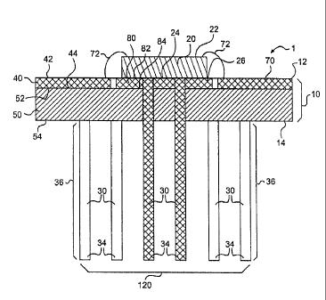
is
directed to a method and device for thermal management in electronic devices
with
printed circuit boards (PCB). The apparatus includes at least one PCB. The PCB
defines a first surface and a second surface, and the PCB may include a metal
layer
and a core. The core may define a first core surface and a second core
surface. The
metal layer may be secured to the first core surface. The apparatus may
include an
electronics package which may be secured to the first surface of the PCB. The
apparatus may include a plurality of pins, each of which may have a first end
and a
second end. The pins may be disposed about the PCB with the first ends
generally
proximate the electronics package such that heat generated by the electronics
package
may be received by the pins generally proximate the first ends. Generally, the
pins
may pass through the core from the first core surface to the second core
surface to
conduct heat generated by the electronics package through the core as heat is
conducted from the first end toward the second end of the pins. A second PCB
may be
spaced apart from the first PCB with the pins securing the first PCB to the
second
PCB.
[0006] The invention may be implemented in a number of ways. According to one
aspect of the invention, an apparatus is provided that includes a first
printed circuit
board (PCB) that includes a first PCB first surface, an electronics package
configured
to be disposed on the first PCB first surface, a second PCB, and a plurality
of pins
configured to secure the first PCB to the second PCB at an interval, the
plurality of
pins being further configured to form an array within the interval, wherein at
least a
2
CA 02706092 2010-05-18
WO 2009/067556
PCT/US2008/084089
portion of the plurality of pins are connectable to the first PCB proximate
the
electronics package to receive at least a portion of heat generated by the
electronics
package and to conduct the portion of heat generated by the electronics
package into
the interval for dispersion.
[0007] In another aspect of the invention, an electrical device is provided
that
includes a first printed circuit board (PCB), an electronics package disposed
on the
first PCB, a second PCB spaced at an interval from the first PCB, the second
PCB
being configured to provide electrical power to the first PCB, and a plurality
of pins
configured to secure the second PCB to the first PCB, wherein the plurality of
pins are
arranged proximate the electronics package to convey heat generated by the
electronics package from the first PCB to the interval for dissipation.
[0008] Additional features, advantages, and embodiments of the invention may
be
set forth or apparent from consideration of the following detailed
description,
drawings, and claims. Moreover, it is to be understood that both the foregoing
summary of the invention and the following detailed description are exemplary
and
intended to provide further explanation without limiting the scope of the
invention as
claimed.
BRIEF DESCRIPTION OF THE DRAWINGS
[0009] The accompanying drawings, which are included to provide a further
understanding of the invention, are incorporated in and constitute a part of
this
specification, illustrate embodiments of the invention and together with the
detailed
3
CA 02706092 2010-05-18
WO 2009/067556
PCT/US2008/084089
description serve to explain the principles of the invention. No attempt is
made to
show structural details of the invention in more detail than may be necessary
for a
fundamental understanding of the invention and the various ways in which it
may be
practiced. In the drawings:
[0010] Figure lA illustrates in plan view an exemplary embodiment of an
apparatus, configured according to principles of the invention;
[0011] Figure 1B illustrates a frontal view of the embodiment of Figure 1A;
[0012] Figure 2A illustrates in plan view an exemplary embodiment of an
apparatus, configured according to principles of the invention;
[0013] Figure 2B illustrates a frontal view the embodiment of Figure 2A;
[0014] Figure 3A illustrates in plan view an exemplary embodiment of an
apparatus, configured according to principles of the invention;
[0015] Figure 3B illustrates a frontal view the embodiment of Figure 3A;
[0016] Figure 4A illustrates in plan view an exemplary embodiment of an
apparatus, configured according to principles of the invention;
[0017] Figure 4B illustrates a frontal view the embodiment of Figure 4A;
[0018] Figure 5A illustrates in plan view an exemplary embodiment of an
apparatus, configured according to principles of the invention;
[0019] Figure 5B illustrates a frontal view the embodiment of Figure 5A;
[0020] Figure 6A illustrates in plan view an exemplary embodiment of an
apparatus, configured according to principles of the invention;
[0021] Figure 6B illustrates a frontal view the embodiment of Figure 6A;
[0022] Figure 7A illustrates in plan view an exemplary embodiment of an
apparatus, configured according to principles of the invention;
[0023] Figure 7B illustrates a frontal view the embodiment of Figure 7A;
4
CA 02706092 2010-05-18
WO 2009/067556
PCT/US2008/084089
[0024] Figure 8A illustrates in plan view an exemplary embodiment of an
apparatus, configured according to principles of the invention;
[0025] Figure 8B illustrates a frontal view the embodiment of Figure 8A:
[0026] Figure 9 illustrates a frontal view of an exemplary embodiment of an
apparatus, configured according to principles of the invention;
[0027] Figures 10A-10F each illustrate in perspective a separate exemplary
embodiment of a pin, configured according to principles of the invention;
[0028] Figure 11A illustrates in top view an exemplary embodiment of an
apparatus according to the present invention;
[0029] Figure 11B illustrates in frontal view an exemplary embodiment of an
apparatus according to the present invention generally corresponding to the
embodiment of Figure 11A;
[0030] Figure 11C illustrates in bottom view an exemplary embodiment of an
apparatus according to the present invention generally corresponding to the
embodiment of Figure 11A;
[0031] Figure 12 illustrates in frontal view an exemplary embodiment of
portions
of an apparatus, constructed according to principles of the invention;
[0032] Figure 13A illustrates in perspective view an exemplary embodiment of a
pin, configured according toyrinciples of the invention;
[0033] Figure 13B illustrates in perspective view another exemplary embodiment
of a pin, configured according to principles of the invention; and
[0034] Figure 14 illustrates in perspective view an exemplary embodiment of an
apparatus, configured according to the principles of the invention.
DETAILED DESCRIPTION OF THE INVENTION
CA 02706092 2010-05-18
WO 2009/067556
PCT/US2008/084089
[0035] The embodiments of the invention and the various features and
advantageous details thereof are explained more fully with reference to the
non-
limiting embodiments and examples that are described and/or illustrated in the
accompanying drawings and detailed in the following description. It should be
noted
that the features illustrated in the drawings are not necessarily drawn to
scale, and
features of one embodiment may be employed with other embodiments as the
skilled
artisan would recognize, even if not explicitly stated herein. Descriptions of
well-
known components and processing techniques may be omitted so as to not
unnecessarily obscure the embodiments of the invention. The examples used
herein
are intended merely to facilitate an understanding of ways in which the
invention may
be practiced and to further enable those of skill in the art to practice the
embodiments
of the invention. Accordingly, the examples and embodiments herein should not
be
construed as limiting the scope of the invention, which is defined solely by
the
appended claims and applicable law. Moreover, it is noted that like reference
numerals represent similar parts throughout the several views of the drawings.
[0036] Referring now to the various embodiments of the Figures, in various
aspects, the apparatus 1 may include a printed circuit board (PCB) 10, which
defines a
first surface 12 and a second surface 14. An electronics package 20 may be
disposed
about the first surface 12 of the PCB 10, and the electronics package 20 may
generate
heat. The PCB 10 may include a metal layer 40 and a core 50, and, in some
aspects,
may include multiple cores 50 interposed between multiple metal layers 40. The
metal
layer 40 may be disposed on a core first surface 52 of the core 50. The metal
layer 40
may include metal such as copper, silver, gold, other metal, or other
conductive
material or combinations thereof suitable to define traces 70, which are
circuit paths
for electronic components affixed to the PCB 10. The core 50 may include any
of the
6
CA 02706092 2010-05-18
WO 2009/067556
PCT/US2008/084089
well known and electrically non-conducting materials commonly used in PCB
manufacture such as FR4. As the core 50 may be electrically non-conducting,
the core
50 may be thermally insulating, and, accordingly, inhibit the transfer of heat
from the
electronics package 20 through the PCB 10.
[0037] The apparatus 1 may include one or more pins 30. Each pin 30 has a
first
end 32 and a second end 34, and is formed from heat conductive material or
combinations of heat conductive materials. A plurality of pins 30 may be
disposed
about the PCB 10 with first ends 32 generally proximate the electronics
package 20
and configured to conduct at least a portion of the heat away from the
electronics
package 20. The pins 30 may be configured with an orientation to pass
generally
through the PCB 10 from the first surface 12 to the second surface 14, with
the first
ends 32 of the pins 30 configured to be positioned generally proximate the
electronics
package 20 to provide paths for heat conduction from the electronics package
20
through the core 50 of the PCB 10. In certain aspects, portions of the pin 30,
including
the second end 34, may extend generally beyond the second surface 14 of the
PCB to
define an extension 36. The extension 36 may disperse or dissipate heat by
convection
and/or radiation. In such aspects, a plurality of pins 30 may include
extensions 36 to
form an array 120 which may further enhance heat dispersal.
[0038] In various aspects, the PCB 10 may include a backplane 60 having a
backplane first surface 62 generally affixed to the core second surface 54 as
shown in
Figures 4B, 5B, 6B, 8B, 9 and 10. The backplane 60 may be comprised of a metal
such as copper, aluminum, graphite, other conductive material, or combinations
thereof. The backplane 60 may function, among other things, to provide a
common
potential for circuitry attached to the PCB 10 and/or to serve as a heat
spreader to
diffuse heat generated by the operation of the circuitry attached to the PCB
10
7
CA 02706092 2010-05-18
WO 2009/067556
PCT/US2008/084089
including the electronics package 20. As such, the backplane 60 may be
electrically
conductive and/or may be thermally conductive.
[0039] In embodiments of the PCB 10 that include the backplane 60, portions of
the pins 30 may be configured to extend into at least portions of the
backplane 60 in
order to transfer heat from the pins 30 into the backplane 60 for dispersal.
The pins 30
may be configured to extend into the backplane 60 to secure, at least in part,
the
backplane 60 to the core 50. In particular, the backplane 60 may include, at
least in
part, graphite, and the pins 30 may be configured to secure such a graphite
backplane
60 to the core 50.
[0040] Each pin 30 may be a generally elongated member such as a nail, screw,
bolt, strip, pin, or the like, and may be configured to conduct heat between
the first
end 32 and the second end 34. Accordingly, each pin 30 may be formed of
copper,
brass, steel, or various other metals, metal alloys, or other heat conductive
materials,
or combinations thereof. The pin 30 may have a generally constant cross-
section
between the first end 32 and the second end 34 or may have, at least in part,
uneven
cross-section. The cross-section of the pin 30 may be substantially
cylindrical, in
some aspects, while, in other aspects, the pin 30 may have, for example, a
polygonal
cross-section such as rectangular or hexagonal cross-section. In still other
aspects, the
pin 30 may have a star shaped cross-section. In other aspects, the pin 30 may
be
flattened proximate the second end 34, perhaps enlarged, to provide a
relatively larger
surface area to increase heat dissipation. A portion of the pin 30, generally
proximate
the first end 32, may form a head 31 that could be, for example, either flat
or rounded.
A portion of the pin 30, generally proximate the second end 34, may generally
define
a point 33. In some aspects, the pin 30 may be configured to be driven into
the PCB
by the application of force about the first end 32. In other aspects, the pin
30 may
8
CA 02706092 2010-05-18
WO 2009/067556
PCT/US2008/084089
include threads and/or configured to be threadedly received into the PCB 10.
In still
other aspects, the pin 30 may be configured to be slidably received in a
channel or
other aperture associated with the PCB 10. The pin 30 may have various
geometric
configurations, include various materials, and may be placed in the PCB 10 in
various
ways as would be recognized by those of ordinary skill in the art upon review
of this
disclosure. Combinations of pins 30 having various lengths, materials, and/or
geometries could be used in some aspects.
[0041] The extension 36 may extend generally beyond the backplane second
surface 64 to disperse heat. Heat may be dispersed from the extension 36 by
free
convection and/or forced convection, as well as by radiation. In various
aspects, a
plurality of extended portions 36 may be configured to form an array 120, and
the
array 120 may dissipate heat by free convection and/or forced convection. In
contrast
to fins or other such structures, air may flow through the array 120 in
multiple
directions to convect heat from the array 120. As would be understood by those
of
ordinary skill in the art upon review of this disclosure, additional
components such as,
for example, fins for heat dispersion and structural members may be secured to
the
backplane second surface 64, and the additional components may be secured, at
least
in part, by one or more pins 30. Also, as would be understood by those of
ordinary
skill in the art upon review of this disclosure, various welds, adhesives,
solders, and
other mechanisms of attachment may be provided to secure various portions of
the
PCB 10 together, so that various adhesive and other layers may be interposed
between
the components in various aspects. For example, the core 50 may be adhesively
secured to the backplane 60, which may interpose an adhesive layer generally
between the core second surface 54 and the backplane first surface 62.
9
CA 02706092 2010-05-18
WO 2009/067556
PCT/US2008/084089
[0042] Figure lA illustrates in plan view an exemplary embodiment of an
apparatus, configured according to principles of the invention, and Figure 1B
illustrates a frontal view of the embodiment of Figure 1A. A PCB 10 may
include a
metal layer 40 and a core 50. The metal layer first surface 42 and portions of
the core
first surface 52 generally define the first surface 12 of the PCB 10, and the
second
surface 14 of the PCB 10 is generally defined by the core second surface 54,
as
illustrated. The metal layer 40 may have a second surface 44.
[0043] An electronics package 20 having a package first surface 22 and a
package
second surface 24 may be disposed about the first surface 12 of the PCB 10, as
illustrated in Figures lA and 1B, with portions of the package second surface
24
biased against portions of the core first surface 52. Traces 70 configured
from the
metal layer 40 may be disposed upon the core first surface 52, and the
electronics
package 20 may be in electrical communication with the traces 70 by electrical
connectors 72, as illustrated. The electrical connectors 72 may be, for
example, power
leads, wire bonds, SMD leads, electrode pads, or the like.
[0044] As further illustrated in Figures lA and 1B, pins 30.1, 30.2 may be
configured to pass through the PCB 10 including the core 50 from the core
first
surface 52 to the core second surface 54 to conduct heat generated by the
electronics
package 20, generally from the first surface 12 to the second surface 14. The
first ends
32.1, 32.2 of pins 30.1, 30.2 may be placed proximate the core first surface
52 and
proximate the package second surface 24 to receive heat from the package
second
surface 24 of the electronics package 20. In some embodiments, portions of the
first
ends 32.1, 32.2 may be generally biased against the package second surface 24.
The
pins 30.1, 30.2 may conduct the heat from the first ends 32.1, 32.2 through
the core 50
from the core first surface 52 to the core second surface 54, and generally to
the
CA 02706092 2010-05-18
WO 2009/067556
PCT/US2008/084089
second ends 34.1, 34.2. As illustrated, portions of the pins 30.1, 30.2,
generally
proximate the second ends 34.1, 34.2, may protrude generally beyond the core
second
surface 54 to define extensions 36.1, 36.2. At least some heat conducted
through the
core 50 from the electronics package 20 may be dispersed, at least in part, by
convection and/or radiation from the extensions 36.1, 36.2. The extensions
36.1, 36.2
may define the array 120, as illustrated. In other embodiments, the second
ends 34.1,
34.2 may lie generally between the core first surface 52 and the core second
surface
54, and/or may be generally proximate the core second surface 54 to disperse
heat
from the core second surface 54.
[0045] Figure 2A illustrates in plan view an exemplary embodiment of an
apparatus, configured according to principles of the invention. Figure 2B
illustrates a
frontal view of the embodiment of Figure 2A. In Figs. 2A and 2B, a PCB 10 that
includes a metal layer 40 and a core 50 is generally illustrated. The metal
layer 40
may include a first surface 42 and portions of the core first surface 52 may
generally
define the first surface 12 of the PCB 10. The second surface 14 of the PCB 10
may
be generally defined by the core second surface 54, as illustrated.
[0046] As illustrated,
portions of the metal layer 40 define traces 70. Other portions
of the metal layer 40 may define a pad 80 having a pad first surface 82 and a
pad second
surface 84, with the pad 80 electrically isolated from the traces 70, as
illustrated. The
electronics package 20 may be disposed about the first surface 12 of the PCB
10, as
illustrated in Figures 2A and 2B, with portions of the package second surface
24
generally abutting portions of the pad first surface 82, so that the
electronics package 20
may be in thermal communication with the pad 80 to distribute heat from the
electronics package 20 into the pad 80. The electronics package 20 may be in
electrical
communication with the traces 70 by electrical connectors 72, as illustrated.
11
CA 02706092 2010-05-18
WO 2009/067556
PCT/US2008/084089
[0047] As further illustrated in Figures 2A and 2B, a plurality of pins 30
may be
configured to be disposed about the pad 80 to conduct heat from the pad 80
through
the core 50. The pins 30 may pass through the PCB 10 including the pad 80 from
the
pad first surface 82 to the pad second surface 84 and through the core 50 from
the
core first surface 52 to the core second surface 54 to conduct heat generally
from the
first surface 12 to the second surface 14. In this implementation, any heat
generated
by the electronics package 20 may be conducted from the package second surface
24
by the pad 80 and distributed to the pins 30 generally proximate the first
ends 32 of
the pins 30. The heat may be conducted through the core 50 from the core first
surface
52 to the core second surface 54 by the pins 30, and the heat dispersed
generally from
the core second surface 54. As illustrated, heat conducted through the core 50
from
the electronics package 20 may be dispersed, at least in part, by convection
and/or
radiation from the extensions 36 of the pins 30. In various implementations,
the
convective heat transfer from the array 120 formed by the extensions 36 may be
either
non-forced or forced.
[0048] In some implementations, at least some pins 30 may pass through the pad
80 from the pad first surface 82 to the pad second surface 84, and the first
ends 32
may be generally proximate the pad first surface 82. In other implementations,
at least
some of the first ends 32 of the pins 30 may be generally proximate the pad
second
surface 84. In still other implementations, at least some of the first ends 32
of the pins
30 may be generally biased against the second surface 84 of the pad 80.
[0049] Figure 3A illustrates in plan view an exemplary embodiment of an
apparatus, configured according to principles of the invention. Figure 3B
illustrates in
frontal view of the embodiment of Figure 3A. In Figures 3A and 3B, a PCB 10
that
includes a metal layer 40 and a core 50 is generally illustrated. The metal
layer first
12
CA 02706092 2010-05-18
WO 2009/067556
PCT/US2008/084089
surface 42 and portions of the core first surface 52 may generally define the
first
surface 12 of the PCB 10. The second surface 14 of the PCB 10 may be generally
defined by the core second surface 54, as illustrated.
[0050] Portions of the metal layer 40 may define traces 70, as illustrated.
Other
portions of the metal layer 40 may define a pad 80 having a pad first surface
82 and a
pad second surface 84, with the pad 80 electrically isolated from the traces
70, as
illustrated in Figures 3A and 3B. As illustrated, a heat slug 90 having a
first heat slug
surface 92 and a second heat slug surface 94 may be secured to the pad 80 with
the
second heat slug surface 94 generally abutting the first pad surface 82. In
this
implementation, the shape of the second heat slug surface 94 may generally
conform
to the shape of the first pad surface 82. The electronics package 20 may be
disposed
about the first surface 12 of the PCB 10, as illustrated, with portions of the
package
second surface 24 biased against portions of the heat slug first surface 82 so
that the
electronics package 20 is in thermal communication with the heat slug 90,
which, in
turn, may be in thermal communication with the pad 80 and, thence, with the
pins 30
generally proximate the first ends 32. The electronics package 20, as
illustrated, may
be in electrical communication with the traces 70 by electrical connectors 72.
[0051] As illustrated in Figures 3A and 3B, the plurality of pins 30 may be
disposed about the pad 80. The pins 30 pass through the PCB 10 including the
core 50
generally from the core first surface 52 to the core second surface 54 to
conduct heat
from the first side 12 to the second side 14 of the PCB 10. In this
implementation,
heat generated by the electronics package 20 may be conducted from the package
second surface 24 through the heat slug first surface 94 into the heat slug
90. Heat
may be conducted from the heat slug second surface 94 through the pad first
surface
82 into the pad 80 to generally distribute heat from the electronics package
20
13
CA 02706092 2010-05-18
WO 2009/067556
PCT/US2008/084089
throughout the heat slug 90 and the pad 80. Heat may be conducted into the
pins 30
generally proximate the first ends 32 of the pins 30 from the pad 80 and/or
the heat
slug 90, and the pins 30 may conduct heat through the core 50 from the core
first
surface 52 to the core second surface 54 to allow the heat to be dispersed
generally
from the core second surface 54, which, in this implementation, defines the
second
surface 14 of the PCB 10.
[0052] In various implementations, the pins 30 may be configured to be in
thermal
communication with the pad 80 and/or with the heat slug 90 by being at least
in part
positioned proximate the pad 80 and/or heat slug 90, by passing through at
least a
portion of the pad 80 and/or heat slug 90, perhaps by being biased against or
otherwise in mechanical contact with or soldered/welded to the pad 80 and/or
the heat
slug 90, or in other ways as would be readily recognized by those of ordinary
skill in
the art upon review of this disclosure, or combinations thereof. As
illustrated in
Figures 3A and 3B, portions of the pins 30 configured to be generally
proximate the
second ends 34 form extensions 36 to disperse heat, at least in part, by
convection
and/or radiation.
[0053] Figures 4A and 4B generally illustrate a PCB 10 that includes the
metal
layer 40, the core 50, and the backplane 60, with the backplane 60 comprising
a heat
conductive material such as, for example, a metal, graphite, or the like. The
metal
layer first surface 42 and portions of the core first surface 52 may be
configured to
generally define the first surface 12 of the PCB 10. The second surface 14 of
the PCB
may be generally defined by the backplane second surface 64, as illustrated.
[0054] The electronics package 20 may be disposed about the first surface 12
of
the PCB 10, as illustrated in Figures 4A and 4B, with portions of the package
second
surface 24 biased against portions of the core first surface 52 or
soldered/welded
14
CA 02706092 2010-05-18
WO 2009/067556
PCT/US2008/084089
thereto to transfer heat by conduction through the package second surface 24
to the
core first surface 52. In other implementations, the package second surface 24
may be
generally set apart, at least in part, from the core first surface 52 so that
heat may be
transferred by radiation and/or convection from the package second surface 24
to the
core first surface 52. Traces 70 configured from the metal layer 40 may be
disposed
upon the core first surface 52, and the electronics package 20 may be in
electrical
communication with the traces 70 by electrical connectors 72, as illustrated.
[0055] The core 50 may be sandwiched between the metal layer 40 and the
backplane 60, as illustrated in Figures 4A and 4B. The core 50, which may be a
thermal and electrical insulator, may inhibit conduction of heat emitted by
the
electronics package 20 to the backplane 60 and, hence, may inhibit the
dispersal of
heat generated by the electronics package 20 from the backplane 60. As
illustrated,
pins 30 may be configured to pass through the core 50 from the core first
surface 52
to the core second surface 54 and through the backplane 60 from the backplane
first
surface 62 to the backplane second surface 64 and beyond to conduct heat from
the
electronics package 30 to the backplane 60 in order to diffuse the heat
generated by
the electronics package 20 throughout the backplane 60. The first ends 32 of
the pins
30 may be placed proximate the package second surface 24 to be in thermal
communication with the package second surface 24 in order to conduct heat
generated
by the electronics package 20 from the package second surface 24 through the
core 50
from the core first surface 52 to the core second surface 54 and into the
backplane 60.
The backplane 60 may disperse the heat generally from the backplane second
surface
64 by convection and/or radiation or the like.
[0056] As illustrated, portions of the pins 30, generally proximate the
second ends
34, may define extensions 36 that protrude generally outward from the
backplane
CA 02706092 2010-05-18
WO 2009/067556
PCT/US2008/084089
second surface 64. Heat may be dispersed, at least in part, by convection
and/or
radiation from the extensions 36.
[0057] Figures 5A and 5B generally illustrate a PCB 10 that includes the metal
layer 40, the core 50, and the backplane 60. The backplane 60 may include a
heat
conductive material. Portions of the metal layer 40 may define traces 70, as
illustrated. Other portions of the metal layer 40 may define a pad 80 having a
pad first
surface 82 and a pad second surface 84, with the pad 80 electrically isolated
from the
traces 70 in the illustrated implementation. The electronics package 20 may be
disposed about the first surface 12 of the PCB 10, as illustrated in Figures
5A and 5B,
with portions of the package second surface 24 generally abutting portions of
the pad
first surface 82 so that the electronics package 20 may be in thermal
communication
with the pad 80. Accordingly, heat generated by the electronics package 20 may
be
distributed throughout the pad 80.
[0058] As illustrated, pins 30 may be disposed about the pad 80 to conduct
heat
from the pad 80 through the core 50 and into the backplane 60 in order to
disperse
heat generated by the electronics package 20 from the backplane 60. The first
ends 32
of the pins 30, in this implementation, may be located generally about the pad
first
surface 82 of the pad 80. The pins 30 may pass through the pad 80 generally
from the
pad first surface 82 to the pad second surface 84, through the core 50 from
the core
first surface 52 to the core second surface 54 and through the backplane 60
from the
backplane first surface 62 to the backplane second surface 64 and extend
outward
from the backplane second surface 64. The backplane 60 may disperse the heat
generally from the backplane second surface 64 by convection and/or radiation.
As
illustrated, portions of the pins 30, generally proximate the second ends 34,
protrude
generally beyond the backplane second surface 64 to form extensions 36. Heat
may be
16
CA 02706092 2010-05-18
WO 2009/067556
PCT/US2008/084089
dispersed by convection and/or radiation from the extensions 36. The pins 30,
in
various implementations, may secure, or at least aid in securing, the
backplane 60 to
the core 50. In implementations wherein the backplane 60 includes graphite,
the pins
30 may be advantageous for securing the graphite backplane 60 to the core. In
various
implementations, the pins 30 may have differing lengths. In various
implementations,
the second ends 24 may be configured to terminate within the backplane 60, or
the
second ends 34 of the pins 30 may be biased against the backplane first
surface 62.
[0059] Figure 6A illustrates in plan view an exemplary embodiment of an
apparatus, configured according to principles of the invention. Figure 6B
illustrates a
frontal view of the embodiment of Figure 6A. The implementation illustrated in
Figures 6A and 6B includes a metal layer 40, a core 50, and a backplane 60.
The
backplane 60 may comprise a heat conductive material. Portions of the metal
layer 40
may define traces 70, as illustrated, while other portions of the metal layer
40 may
define the pad 80. The pad 80 may be electrically isolated from the traces 70.
Also, as
illustrated in Figures 6A and 6B, a heat slug 90 having a first heat slug
surface 92 and
a second heat slug surface 94 may be secured to the pad 80 with the second
heat slug
surface 94 generally abutting the first pad surface 82. The electronics
package 20 may
be configured to be disposed about the first surface 12 of the PCB 10, as
illustrated,
with portions of the package second surface 24 biased against portions of the
heat slug
first surface 82 so that the electronics package 20 may be in thermal
communication
with the heat slug 90 to distribute heat generated by the electronics package
20
throughout the heat slug 90 and pad 80. Pins 30 may pass through the pad 80,
the core
50, and the backplane 60 to conduct heat generated by the electronics package
20
from the pad 80 and heat slug 90 to the backplane 60 for dispersal. Heat may
be
17
CA 02706092 2010-05-18
WO 2009/067556
PCT/US2008/084089
dispersed, at least in part, by convection and/or radiation from the
extensions 36 that
form array 120 in this implementation.
[0060] Figure 7A illustrates in plan view an exemplary embodiment of an
apparatus, configured according to principles of the invention. Figure 7B
illustrates a
frontal view of the embodiment of Figure 7A. In this implementation, one or
more
pins 30 may be configured to pass at least partially through the trace(s) 70.
As
illustrated, the PCB 10 may include the metal layer 40 from which the traces
70 are
configured, and the core 50. Pins 30 may be disposed about the electronics
package
20 to conduct heat generated by the electronics package 20 from the first
surface 12 to
the second surface 14 to be dispersed. Pins 30 that pass at least partially
through the
traces 70 may pass at least partially into the core 50. The core 50 may
electrically
isolate the pins 30 so that substantially no short circuiting may occur
through the core
50 between pins 30 when having differing potentials.
[0061] In other implementations that include the pad 80, the pad 80 may be
electrically charged in order to supply power to the electronics package 20.
Pins 30
that may contact the pad 80 in such implementations would be electrically
isolated by
the core so that substantially no short circuiting occurs through the core 50
between
pins 30 when having differing potentials.
[0062] Figure 8A illustrates in plan view an exemplary embodiment of an
apparatus, configured according to principles of the invention. Figure 8B
illustrates a
frontal view the embodiment of Figure 8A. One or more pins 30 may pass through
the
trace(s) 70, as illustrated in Figures 8A and 8B. Also, as illustrated, the
PCB 10 may
include the metal layer 40 from which the traces 70 may be configured, the
core 50,
and the backplane 60. Pins 30 may be disposed about the electronics package 20
to
conduct heat generated by the electronics package from the first surface 12 to
the
18
CA 02706092 2010-05-18
WO 2009/067556
PCT/US2008/084089
second surface 14 for dispersal. Pins 30 that pass through the traces 70 may
pass into
the core 50. The core 50 may electrically isolate the pins 30 so that
substantially no
short circuiting occurs through the core 50 between pins 30, when they have
differing
potentials. As illustrated, the backplane 60 may include backplane cavities 66
that
pass about respective pins 30 so that the pins 30 do not contact (i.e., are
isolated from)
the backplane 60 in order to prevent short circuiting between pins 30 through
the
backplane 60. The backplane cavities 66 may include a non-conducting or
insulating
material. The pins 30 may exchange heat with the backplane 60 by radiation
and/or
convection, and the pins 30 may also generally disperse heat through the
portions of
the pins 30 proximate the second ends 34 by radiation and/or convection in
this
implementation.
[0063] Because of the backplane cavities 66, the pins 30 do not directly
contact the
backplane 60, which may limit the heat conductance between the pins 30 and the
backplane 60. In an alternative implementation, the pins 30 may be anodized or
chemically treated, at least in part, so that the surfaces of the pins 30 are
electrically
non-conductive. The anodized pin 30 may pass through the trace 70, through the
core
50 and into the backplane 60, perhaps with mechanical contact between the pins
30
and the backplane 60, to conduct heat generated by the electronics package
from the
first surface 12 to the backplane 60 without short circuiting. Similarly, in
implementations wherein the pad 80 may be electrically charged, anodized pins
30
may electrically contact the pad 80 at the end 32 and contact the backplane 60
without
short circuiting.
[0064] Figure 9 illustrates a frontal view of an exemplary embodiment of an
apparatus, configured according to principles of the invention. As shown in
this
implementation, pins 30.1, 30.2 may pass through the PCB 10 including the core
50 to
19
CA 02706092 2010-05-18
WO 2009/067556
PCTMS2008/084089
conduct heat generated by the electronics package 20 generally from the first
surface
12 to the second surface 14. The pins 30.1, 30.2 may be configured to be
disposed
proximate the electronics package 20 and configured to be in thermal
communication
with the electronics package 20 so that heat generated by the electronics
package 20
may be conducted through the package second surface 14 into the pins 30.1,
30.2
generally proximate the first ends 32.1, 32.2. The pins 30.1, 30.2 may conduct
heat
through the core 50 from the core first surface 52 to the core second surface
54. The
pins 30.1, 30.2 may pass through the backplane 60, and heat may be conducted
from
the pins 30.1, 30.2 into the backplane 60. The backplane 60, in this
implementation,
may include graphite which conducts heat anisotropically. The preferred
directions
for heat conduction in the backplane 60, in this implementation, are parallel
to the
planes defined by the backplane first surface 62 and the backplane second
surface 64.
Thus, the backplane 60 may conduct heat from pins 30.1, 30.2, to pins 30.3,
30.4,
30.5, and heat may be generally dispersed by convection and/or radiation from
the
extensions 36.3, 36.4, 36.5 that protrude beyond the backplane second surface
64. As
illustrated, heat conducted through the core 50 from the electronics package
20 may
be dispersed, at least in part, by convection and/or radiation from the
extensions 36.1,
36.2.
[0065] Figures 10A-10F each illustrate in perspective view a separate
exemplary
embodiment of a pin, configured according to principles of the invention.
[0066] Figure 10A illustrates a pin 30 configured to have a generally rounded
head
31 at the first end 32. The pin 30 illustrated in Figure 10B has a generally
flat head 31
at the first end 32 and the second end 34 may be configured with a point 33.
The pins
30 illustrated in Figures 10C, 10D, 10E, and 1OF have generally square,
generally
rectangular, hexagonal, and star shaped cross-sections, respectively. The pin
30 may
CA 02706092 2010-05-18
WO 2009/067556
PCT/US2008/084089
assume other shapes and configurations as would be recognized by those of
ordinary
skill in the art upon review of this disclosure.
[0067] Methods, in various aspects, may include arranging the apparatus 1, PCB
10, metal layer 40, core 50, and/or electronics package 20 with the pins 30.
Further
the method may include generating heat proximate the first surface 12 of the
PCB 10
by an electronics package 20 and may include conducting the heat from the
first
surface 12 to the second surface 14, at least in part, using a plurality of
pins 30. The
methods may include dispersing heat from an array 120 defined by a plurality
of
extensions 36. The methods may include securing the backplane 60, at least in
part by
a plurality of pins 30.
[0068] In the apparatus described above, the electronics package 20 may
include
one or more lighting devices, computing devices, memory storage devices,
communication devices, and/or the like. For example, the lighting devices may
include LEDs and any associated electronics.
[0069] Further, with respect to the aspects described above, the apparatus
1 may be
light, a computer, a storage device, a telecommunications device or the like,
or any
combination thereof.
[0070] Figures 13A, 13B, and 13C illustrate an exemplary implementation that
may include a first PCB 210 and a second PCB 220, with the first PCB 210 set
apart
and secured at an interval 230 from the second PCB 220 by a plurality of pins
30. One
or more LEDs 250 may be surface mounted to the first PCB first surface 212.
The
second PCB 220 may be configured to include a driver circuit 395 that may
provide
regulated electrical power to each of the one or more LEDs 250, in the
illustrated
exemplary implementation. As illustrated, the pins 30 may be disposed about
the first
PCB 210 such that portions of the pins 30, generally proximate the first ends
32, may
21
CA 02706092 2010-05-18
WO 2009/067556
PCT/US2008/084089
be in thermal communication with the one or more LEDs 250 in order to conduct
at
least a portion of the heat generated by the one or more LEDs 250 through the
first
PCB 210 from the first PCB first surface 212 to the first PC second surface
214 to
disperse the at least a portion of the generated heat generally away from the
first PCB
second surface 214. The plurality of pins 30 may form an array 260 between the
first
PCB second surface 214 and the second PCB first surface 222 through which air
flow
397, perhaps including the flow of other heat transfer media, may pass. Heat
conducted by the one or more pins 30 from the one or more LEDs 250 through the
first PCB 210 from the first PCB first surface 212 to the first PCB second
surface 214
may be dispersed from the array 250 by either free or forced convective air
flow 397
through the array 260. Heat may also be dispersed from the array 260 by
radiation.
[0071] Figure 12 illustrates in frontal view an exemplary embodiment of
portions
of an apparatus, constructed according to principles of the invention. As
illustrated in
Figure 12, the first PCB 210 may include a first core 270 interposed between a
first
metal layer 280 and a second metal layer 290. In this illustrated
implementation, a
first metal layer second surface 284 may be generally biased against a first
core first
surface 272, and a second metal layer first surface 292 may be generally
biased
against the first core second surface 274 to form the first PCB 210. As would
be
understood by those of ordinary skill in the art upon review of this
disclosure, various
adhesives and other materials may be interposed between the first metal layer
second
surface 284 and the first core first surface 272, and/or between the first
core second
surface 274 and the second metal layer first surface 292. In other
implementations, as
would be recognized by those of ordinary skill in the art upon review of this
disclosure, the first PCB 210 could include multiple cores with interposed
metal
layers. Moreover, in alternate implementations, the metal layer of the
embodiments
22
CA 02706092 2010-05-18
WO 2009/067556
PCT/US2008/084089
herein might be equivalently implemented by any suitable conducting material,
perhaps including a non-metallic material that is suitable to be successfully
adapted
for applying to the first core first surface 272.
[0072] First traces 286 configured from the first metal layer 280 may be
disposed
upon the first core first surface 272 such that portions of the first core
first surface 272
and portions of the first metal layer first surface 282 define the first PCB
first surface
212 as illustrated in Figure 11A. In various implementations, the first metal
layer first
surface 282 may be covered by a masking material so that the masking material
and/or the first core first surface 272 define the first PCB first surface
212. The first
metal layer first surface 282 may, in various implementations, be plated,
coated, or
otherwise treated, for example, to prevent oxidation. The LEDs 250, in this
implementation, may be disposed about the first PCB first surface 212 to be in
electrical communication with the first traces 286.
[0073] Similarly, in this exemplary implementation, second traces 296
configured
from the second metal layer 290 may be disposed upon the first core second
surface
274 such that portions of the first core second surface 274 and portions of
the second
metal layer second surface 294 may define the first PCB second surface 214. In
various implementations, the second metal layer second surface 294 may be
covered
by a masking material so that the masking material and/or the first core
second
surface 274 define the first PCB second surface 214. The second traces 296
disposed
upon the first core second surface, in this implementation, mirror the first
traces 286
disposed upon the first core first surface 272, and the first traces 286 and
the second
traces 296 may be in electrical communication.
[0074] As illustrated in Figure 12, the second PCB 220 may include a second
core
300 interposed between a third metal layer 310 and a fourth metal layer 320.
In this
23
CA 02706092 2010-05-18
WO 2009/067556
PCT/US2008/084089
illustrated example, a third metal layer second surface 314 may be generally
biased
against the second core first surface 302, and a fourth metal layer first
surface 322
may be generally biased against the second core second surface 304 to form the
second PCB 220. As would be understood by those of ordinary skill in the art
upon
review of this disclosure, various adhesives and other materials may be
interposed
between the third metal layer second surface 314 and the second core first
surface
302, and/or between the second core second surface 304 and the fourth metal
layer
first surface 322. In other implementations, as would be recognized by those
of
ordinary skill in the art upon review of this disclosure, the second PCB 220
could
include multiple cores with interposed metal layers.
[0075] One or more third traces 316 configured from the third metal layer 310
may
be disposed upon the second core first surface 302 such that portions of the
second
core first surface 302 and portions of the third metal layer first surface 312
define the
second PCB first surface 222 in the illustrated exemplary implementation. In
various
implementations, the third metal layer first surface 312 may be covered by a
masking
material so that the masking material and/or the second core first surface 302
define
the second PCB first surface 222.
[0076] Fourth traces 326 configured from the fourth metal layer 320 may be
disposed upon the second core second surface 304 such that portions of the
second
core second surface 304 and portions of the fourth metal layer second surface
324
may define the second PCB second surface 224. In various implementations, the
fourth metal layer second surface 324 may be covered by a masking material so
that
the masking material and/or the second core second surface 304 may define the
second PCB second surface 224. One or more of the fourth traces 326 disposed
upon
the second core second surface 304, in this implementation, may be in
electrical
24
CA 02706092 2010-05-18
WO 2009/067556
PCT/US2008/084089
communication with one or more of the third traces 316 disposed upon the
second
core first surface 302.
[0077] The first core 270 and the second core 300 may comprise an electrically
insulating material that may also be thermally insulating. Accordingly, the
pins 30
may provide a path for efficient heat conduction through the first core 270
and/or
through the second core 300.
[0078] In the illustrated exemplary implementation, a first power connector
342
and a second power connector 344 are received into the second PCB 220 and
extend
forth from the second PCB 220 to communicate electric power from a source to
the
second PCB 220. The second PCB 220 may include a driver circuit 395 configured
to
receive electric power from the source and to provide regulated electric power
to the
one or more LEDs 250 secured to the first PCB 210. The driver circuit 395 may
include one or more electronics packages 346, which may be disposed about the
second PCB first surface 222 and/or the second PCB second surface 224, as
illustrated
in Figure 11C.
[0079] In the implementations, the first ends 32 of the pins 30 may be
received in
the first PCB 210 and the second ends 34 of the pins 30 may be received in the
second
PCB 220 to secure the first PCB 210 to the second PCB 220 at the interval 230,
as
illustrated. Also as illustrated, the first ends 32 of the pins 30 may be
disposed
generally about the first PCB first surface 212 and the second ends 34 of the
pins 30
may be disposed about the second PCB second surface 224.
[0080] The pins 30 may form an array 260 in the interval 230 between the first
PCB second surface 214 and the second PCB first surface 222, and the pins 30
may
be set apart such that air flow 397 may pass around and through the array 260
to
disperse heat from the array 260. As illustrated in Figure 11B, the surfaces
35 of
CA 02706092 2010-05-18
WO 2009/067556
PCT/US2008/084089
adjacent pins 30 may define gap 397, where the gap 397 may be sufficient for
air to
flow through to disperse heat from the pins 30 by convection.
[0081] At least a portion of the pins 30 generally proximate the first ends 32
may
be in thermal communication with the LEDs 250 in order to conduct a portion of
the
heat generated by the LEDs 250 from the first PCB first surface 212 through
the first
core 270 to the first PCB second surface 214 for dispersal, at least in part,
from the
array 260. The second ends 34 of the pins 30 may, in some implementations, be
in
thermal communication with one or more electronics packages 346 secured to the
second PCB second surface 224 to conduct at least a portion of the heat
generated by
the electronics packages 346 from the second PCB second surface 224 to the
second
PCB first surface 222 for dispersal from the array 260. In various
implementations,
one or more pins 30 may be in thermal communication with one or more
electronics
packages 346 disposed about the first PCB second surface 214 and/or disposed
about
the second PCB first surface 222 to communicate at least a portion of the heat
from
the one or more electronics packages 346 to the array 260 for dispersal.
[0082] As illustrated, a pin 350 may engage a third trace 316 and/or a
fourth trace
326 on the second PCB 220 and may engage a first trace 286 and/or a second
trace
296 on the first PCB 210 such that the first PCB 210 and the second PCB 220
may be
in electrical communication. Accordingly, the driver circuit 395 configured on
the
second PCB 220 may communicate regulated power, for example, to drive the one
or
more LEDs 250 attached to the first PCB 210 through third trace 316 and/or
fourth
trace 326, through the pin 350 to the first trace 286 and/or second trace 296,
and,
thence, to one or more LEDs 250.
[0083] For example, a first via 360 is defined by a first conductive layer
362 and
extends from the first PCB first side 212 to the first PCB second side 214, as
26
CA 02706092 2010-05-18
WO 2009/067556
PCT/US2008/084089
illustrated in Figure 12. The first conductive layer 362 may be composed of a
metal
such as copper or other electrically conductive material and is configured to
place the
second trace 296 in electrical communication, as illustrated. The first trace
286 and
the second trace 296 arc in electrical communication with LED 250 through the
LED
connector 251 secured to the first trace 286, as illustrated.
[0084] Portions of the pin 350 generally proximate the first pin end 352
are
received in the first via 360 and secured by solder 364 in this
implementation.
Portions of the pin 350 generally proximate the first pin end 352 may be "star
shaped"
or otherwise configured in various ways as would be recognized by those of
ordinary
skill in the art upon review of this disclosure to take up solder. The first
trace 286 and
the second trace 296 may electrically communicate through the pin 350, in this
implementation, as well as
through the first conductive layer 362, and the first trace 286 and the second
trace 296
may electrically communicate with the driver circuit 395 on the second PCB 220
through
the pin 350.
[0085] As illustrated in Figure 12, a second via 361 is defined by a second
conductive layer 363 and extends from the second PCB first side 222 to the
second
PCB second side 224. The second conductive layer 363 may be composed of a
metal
such as copper or other electrically conductive material, and is configured to
place the
third trace 316 and the fourth trace 226 in electrical communication, as
illustrated.
Portions of the pin 350 generally proximate the second pin end 354 are
received in the
second via 361 and secured by solder 364 in this implementation. The driver
circuit
395 may be in electrical communication with the third trace 316 and/or the
fourth
27
CA 02706092 2010-05-18
WO 2009/067556
PCT/US2008/084089
trace 326 and, as a consequence, with the LED 250 on the first PCB 210 through
the
pin 350.
[0086] As illustrated in Figures 11B and 14, an assembly 370 may include
the first
PCB 210 with one or more LEDs 250 disposed about the first PCB first surface
212,
the second PCB 220 with the second PCB 220 configured to include the driver
circuit
395, and with the first PCB 210 securably held at the interval 230 from the
second
PCB 220 by a plurality of pins 30 that form array 260. Optionally, the
assembly 370
may be positioned in a housing 380. The housing 380, in this exemplary
implementation, may be configured to receive the assembly 370 and to maintain
orientation of the LEDs 250 in order to direct light emitted from the LEDs
250. The
housing 380 may define one or more apertures 385, and air flow 397 may pass
through the one or more apertures 385, as indicated, either by free convection
or by
forced convection to disperse heat from the array 260. Heat may be dispersed
from
the array 260 by radiation through the one or more apertures 385.
[0087] The one or more apertures 385 may be disposed circumferentially about
the
optional housing 380 such that the air flow 397 may pass through the one or
more
apertures 385 and through the array 260 generally normal to an axis 392 of the
pins
30, as illustrated in Figure 14. In implementations wherein the pins 30 may be
substantially symmetrical about the axis 392, as illustrated in Figure 13A for
example,
the pins 30 may be oriented such that the axis 392 may be more or less
perpendicular
to the air flow 397, and the air flow 397 may be at any circumferential
orientation
with respect to the axis 392. In other implementations, the pins 30 may have,
for
example, a generally rectangular configuration, perhaps with increased surface
area,
and may be oriented such that the air flow 397 may pass generally parallel to
the
rectangular surface 35, as illustrated in Figure 13B.
28
CA 02706092 2010-05-18
WO 2009/067556
PCT/US2008/084089
[0088] In operation, the one or more LEDs 250 attached to the first PCB
first
surface 212 may generate heat. Pins 30 may thermally communicate with the one
or
more LEDs 250 to conduct heat from the one or more LEDs through the first PCB
210 from the first PCB first surface 212 to the first PCB second surface 214
and to
disperse the heat from the array 260 in the interval 230 between the first PCB
second
surface 214 and the second PCB first surface 222. In some implementations, air
flow
397 may be provided by forced convection to disperse the heat from the array
260, at
least in part. In other implementations, air flow 397 by free convection may
be
provided to disperse the heat from the array 260, at least in part. In various
implementations, one or more pins 30 may be in thermal communication with one
or
more electronics packages 346 secured to the first PCB first surface 212, the
first PCB
second surface 214, the second PCB first surface 222, and/or the second PCB
second
surface 224 to dissipate heat from the one or more electronics packages 346
from the
array 260 in the interval 230. In various implementations, the driver circuit
395 may
be configured onto the second PCB 220 and may electrically communicate with
one
or more LEDs 250 on the first PCB, at least in part, by one or more pins 350.
[0089] Methods, in various aspects, may include generating heat proximate the
first surface 12 of the PCB 10 by an electronics package 20 and may include
conducting the heat from the first surface 12 to the second surface 14, at
least in part,
using a plurality of pins 30. The methods may include dispersing heat from any
array
120 defined by a plurality of extensions 36. The methods may include securing
the
backplane 60, at least in part, by a plurality of pins 30.
[0090] In the apparatus described above, the one or more electronics packages
346
may include one or more lighting devices, computing devices, memory storage
devices, communication devices, and/or the like. For example, the lighting
devices
29
CA 02706092 2013-11-19
may be LEDs and any associated electronics. Further, with respect to the
aspects described
above, the assembly 370 may comprise a light, a computer, a storage device, a
telecommunications device or the like, or any combination thereof.
[0091] In accordance with various embodiments of the invention, the methods
described
herein are intended for operation with dedicated hardware implementations
including, but not
limited to, semiconductors, application specific integrated circuits,
programmable logic arrays,
and other hardware devices constructed to implement the methods and modules
described
herein.
[0092] The scope of the claims should not be limited by the preferred
embodiments set forth in
the examples, but should be given the broadest interpretation consistent with
the description as
a whole, which simply notes that the claims are not to be limited to the
preferred or
exemplified embodiments of the invention, is permissible.