Note: Descriptions are shown in the official language in which they were submitted.
CA 02706434 2010-05-20
WO 2009/070240 PCT/US2008/012980
-1-
SEPARATION OF NANOSTRUCTURES
FIELD OF THE INVENTION
The present invention generally relates to systems and methods for the
separation
of nanostructures and, particularly, for the separation of populations of
nanostructures
from other populations of nanostructures based upon differences in density.
RELATED APPLICATIONS
This application claims the benefit of U.S. Provisional Patent Application
Serial
No. 61/004,009, filed November 21, 2007, entitled "Separation of
Nanostructures," by
Strano, et al., incorporated herein by reference in its entirety.
BACKGROUND
A variety of nanostructures have been envisioned for use in industries ranging
from structural materials to electronic devices. For example, carbon nanotubes
have
been highlighted as novel sources for future nano-electronics. Carbon
nanotubes may
have high aspect ratios with small diameters, 103 times higher electronic
current carrying
capacity (109A/cm2) than that of the noble metals, two times higher thermal
conductivity
(6600 W/mK) than that of pure diamond, and they may be ballistic conductors at
room
temperature over many microns. Carbon nanotubes may be either metallic or
semiconducting depending on the way in which the graphene sheet is rolled to
form the
desired nanotube. Both metallic and semiconducting carbon nanotubes have
potential
for widespread applications, ranging from ultra-low resistance materials,
transparent
conductors, and electrical interconnects in the case of metallic carbon
nanotubes.
Semiconducting carbon nanotubes are desired for field-effect transistors
applications.
Carbon nanotubes are usually produced by synthetic protocols as mixtures of
all
electronic types. Therefore, the separation and electronic sorting of carbon
nanotubes
remains a substantial barrier to widespread electronic and optical
applications of these
and similar materials.
Accordingly, improved materials and methods are needed.
CA 02706434 2010-05-20
WO 2009/070240 PCT/US2008/012980
-2-
SUMMARY OF THE INVENTION
The present invention relates generally to the separation of populations of
nanostructures from other populations of nanostructures based upon differences
in
density. The subject matter of the present invention involves, in some cases,
interrelated
products, alternative solutions to a particular problem, and/or a plurality of
different uses
of one or more systems and/or articles.
In some embodiments a method for separating nanostructures is described
wherein the method comprises providing a plurality of nanostructures, exposing
the
nanostructures to a diazonium salt such that a first population of the
plurality of
nanostructures reacts with the diazonium salt and a second population of the
plurality of
nanostructures does not react with the diazonium salt, and separating the
first and second
populations based upon a difference in density.
In one set of embodiments, a method for separating nanostructures is described
wherein the method comprises exposing a plurality of nanostructures to a set
of
conditions under which a first population of the plurality of nanostructures
is modified in
a manner affecting the density of individual members of that population
differently than
a second population of the plurality of nanostructures, and separating the
first and second
populations using a centrifuge with a relative centrifugal force of less than
about
100,000 g.
In some embodiments, a method for separating nanostructures is described
wherein the method comprises exposing a plurality of nanostructures to a set
of
conditions under which a first population of the plurality of nanostructures
is modified
such that the average density of the individual members of the first
population is at least
about 100 kg/m3 greater than the average density of the individual members of
a second
population of nanostructures, and separating the first and second populations
based upon
the difference in densities.
In one set of embodiments, a method for separating nanostructures is described
wherein the method comprises exposing a plurality of nanostructures to a set
of
conditions under which a first population of the plurality of nanostructures
is modified
such that the average density of the individual members of the first
population is at least
about 10% greater than the average density of the individual members of a
second
CA 02706434 2010-05-20
WO 2009/070240 PCT/US2008/012980
-3-
population of nanostructures, and separating the first and second populations
based upon
the difference in densities.
Other aspects, embodiments and features of the invention will become apparent
from the following detailed description when considered in conjunction with
the
accompanying drawings. The accompanying figures are schematic and are not
intended
to be drawn to scale. For purposes of clarity, not every component is labeled
in every
figure, nor is every component of each embodiment of the invention shown where
illustration is not necessary to allow those of ordinary skill in the art to
understand the
invention. All patent applications and patents incorporated herein by
reference are
incorporated by reference in their entirety. In case of conflict, the present
specification,
including definitions, will control.
BRIEF DESCRIPTION OF THE DRAWINGS
Non-limiting embodiments of the present invention will be described by way of
example with reference to the accompanying figures, which are schematic and
are not
intended to be drawn to scale. In the figures, each identical or nearly
identical
component illustrated is typically represented by a single numeral. For
purposes of
clarity, not every component is labeled in every figure, nor is every
component of each
embodiment of the invention shown where illustration is not necessary to allow
those of
ordinary skill in the art to understand the invention. In the figures:
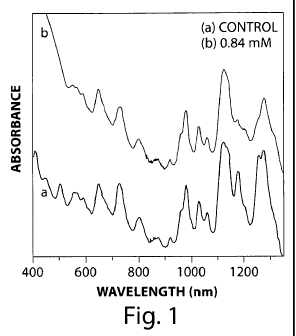
FIG. 1 includes UV-vis-nIR absorption spectra of (a) a control sample and (b)
a
0.84 nM reaction sample of functionalized nanostructures, according to one set
of
embodiments;
FIG. 2 includes photographs of centrifuge tubes after centrifugation,
according to
one set of embodiments;
FIG. 3 is, according to one set of embodiments, a plot of density measurement
of
functionalized and non-functionalized nanostructures; and
FIG. 4 includes plots of Raman measurements of nanostructures, according to
one set of embodiments.
CA 02706434 2010-05-20
WO 2009/070240 PCT/US2008/012980
-4-
DETAILED DESCRIPTION
The present invention generally relates to the separation of one or more
populations of nanostructures from one or more other populations of
nanostructures
based upon differences in density. An overall mixture of very similar or
identical
nanostructures may be exposed to a set of conditions under which one
population of the
nanostructures is affected differently than the other, allowing separating on
the basis of
differences in density.
Synthetic methods of fabricating nanostructures (e.g., carbon nanotubes) often
lead to mixtures with diverse physical and chemical properties (e.g., bandgap,
conductivity, etc.). The ability to purify a population of nanostructures
based on their
properties may be useful in many industries. For example, carbon nanotubes may
be
useful in producing transparent conductive layers which may be used, for
example, in
displays (e.g., LCDs, plasma displays, vacuum fluorescent displays, field
emission
displays, touch panels, etc.), organic light-emitting diodes, antistatic
coatings, electrodes
of power supplies (e.g., photovoltaic cells, lithium ion batteries, etc.),
hydrogen storage
units in fuel cells, sensors (e.g., gas and biological sensors), and
interconnects in memory
devices, among others. The ability to obtain a sample of nanostructures with
similar
physical or chemical properties may play an important role in the development
of such
technologies. For example, by separating conductive carbon nanotubes from semi-
conductive and non-conductive carbon nanotubes, one could manufacture thinner
films
with conductivities as high or higher than thicker films made with an
unpurified mixture
of carbon nanotubes. One of ordinary skill in the art can imagine other
applications in
which it would be desirable to separate a population of nanostructures from a
mixture
based on other physical or chemical properties.
In all embodiments described herein, the degree of separation of one
population
from a different population of a mixture of nanostructures is either made
possible at all,
or improved after exposure to the conditions described. For example, a mixture
of
nanostructures may exist in which, inherently, prior to the technique of the
invention,
separation of one population from another on the basis of differences in
density may be
effectively impossible or may be possible only to a very small degree. After
exposure to
the appropriate conditions, the ability to separate one population from
another either
improves to the point that separation can be carried out in a measurable
manner, or
CA 02706434 2010-05-20
WO 2009/070240 PCT/US2008/012980
-5-
improves to the point that one population can be separated effectively
entirely from the
other. Specifically, in one embodiment, a mixture of nanostructures includes
at least two
different populations which, prior to exposure to the conditions, can be
separated only to
no more than about 20% completion. In this context, "completion" means
complete
separation of one population from another, and X% completion means that only
X% of
any population of the mixture having a distinct characteristic from the other
is separable
from the other. However, after exposure to the conditions, in accordance with
the
invention, separation of the nanostructures on the basis of density can occur
to at least
50% completion or, in other embodiments, at least 70%, 80%, 90%, 95%, or
greater than
98% completion.
As used herein, the term "nanostructure" refers to articles having a fused
network
of atomic rings, and at least one cross-sectional dimension of less than about
1 m, less
than about 500 nm, less than about 250 nm, less than about 100 nm, less than
about
75 nm, less than about 50 nm, less than about 25 nm, less than about 10 nm,
or, in some
cases, less than about 1 nm. In some instances, the nanostructures described
herein are
single molecules. In some embodiments, the nanostructures described herein
have a
maximum cross-sectional dimension of less than about 1 m, less than about 500
nm,
less than about 250 nm, less than about 100 nm, less than about 75 nm, less
than about
50 nm, less than about 25 nm, less than about 10 nm, or, in some cases, less
than about
1 nm. As used herein, the "maximum cross-sectional dimension" refers to the
largest
distance between two opposed boundaries of an individual structure that may be
measured.
In some embodiments, carbon-based nanostructures are described. As used
herein, a "carbon-based nanostructure" comprises a fused network of aromatic
rings, the
network comprising a plurality of double bonds, wherein the nanostructure
comprises
carbon. In some embodiments, the carbon-based nanostructures may comprise at
least
about 40%, at least about 50%, at least about 60%, at least about 70%, at
least about
80%, at least about 90%, or at least about 95% of carbon by mass, or more. In
some
instances, the nanostructures have a cylindrical, pseudo-cylindrical, or horn
shape. In
some embodiments, the carbon-based nanostructure comprises a fused network of
at
least 10, at least 20, at least 30, at least 40, or, in some cases, at least
50 aromatic rings.
CA 02706434 2010-05-20
WO 2009/070240 PCT/US2008/012980
-6-
In some cases, the carbon-based nanostructure may comprise an elongated
chemical structure having a diameter on the order of nanometers and a length
on the
order of microns (e.g., tens or microns, hundreds of microns, etc.), resulting
in an aspect
ratio greater than 10, 100, 1000, 10,000, or greater. In some cases, the
nanostructure
may have a diameter less than 1 m, less than 100 nm, 50 nm, less than 25 nm,
less than
nm, or, in some cases, less than 1 nm. Carbon-based nanostructures may have a
cylindrical or pseudo-cylindrical shape, in some cases, such as a carbon
nanotube.
The carbon-based nanostructures may be substantially planar or substantially
non-planar, or may comprise a planar or non-planar portion. The carbon-based
nanostructures may optionally comprise a border at which the fused network
terminates.
For example, a sheet of graphite is a planar carbon-containing molecule
comprising a
border at which the fused network terminates, while a carbon nanotube is a
nonplanar
carbon-based nanostructure with borders at either end. In some cases, the
border may be
substituted with hydrogen atoms. In some cases, the border may be substituted
with
groups comprising oxygen atoms (e.g., hydroxyl). In other cases, the border
may be
substituted as described herein. The term "fused network" might not include,
for
example, a biphenyl group, wherein two phenyl rings are joined by a single
bond and are
not fused. In some cases, the fused network may substantially comprise carbon
atoms.
In some cases, the fused network may comprise carbon atoms and heteroatoms.
Some
examples of carbon-based nanostructures include graphene, carbon nanotubes
(e.g.,
single-walled carbon nanotubes (SWNTs), multi-walled carbon nanotubes
(M)VNTs)),
carbon nanowires, carbon nanoribbons, carbon nanohorns, and the like.
In some embodiments, the nanostructures comprise non-carbon nanotubes. Non-
carbon nanotubes may be of any of the shapes and dimensions outlined above
with
respect to carbon nanotubes. The non-carbon nanotube material may be selected
from
polymer, ceramic, metal and other suitable materials. For example, the non-
carbon
nanotube may comprise a metal such as Co, Fe, Ni, Mo, Cu, Au, Ag, Pt, Pd, Al,
Zn, or
alloys of these metals, among others. In some instances, the non-carbon
nanotube may
be formed of a semi-conductor such as, for example, Si. In some cases, the non-
carbon
nanotubes may be Group II-VI nanotubes, wherein Group II consists of Zn, Cd,
and Hg,
and Group VI consists of 0, S, Se, Te, and Po. In some embodiments, non-carbon
nanotubes may comprise Group III-V nanotubes, wherein Group III consists of B,
Al,
CA 02706434 2010-05-20
WO 2009/070240 PCT/US2008/012980
-7-
Ga, In, and Ti, and Group V consists of N, P, As, Sb, and Bi. As a specific
example, the
non-carbon nanotubes may comprise boron-nitride nanotubes.
In some embodiments, the nanostructures comprise both carbon and another
material. For example, in some cases, a multi-walled nanotube may comprise at
least
one carbon-based wall (e.g., a conventional graphene sheet joined along a
vector) and at
least one non-carbon wall (e.g., a wall comprising a metal, silicon, boron
nitride, etc.).
In some embodiments, the carbon-based wall may surround at least one non-
carbon wall.
In some instances, a non-carbon wall may surround at least one carbon-based
wall.
A variety of nanostructures can be separated in accordance with the invention,
from mixtures of similar nanostructures. Mixtures of nanotubes, nanowires,
nanoparticles, colloidal particles, and the like can be separated according to
the
technique. The technique finds particular use when the initial mixture
includes all like
types of nanostructures, e.g., a mixture where all nanostructures are
nanotubes, or a
mixture where all nanostructures are colloidal particles, or the like.
Initially, the mixture,
in accordance with the invention, includes at least two populations having a
difference in
a characteristic rendering them desirably separable from each other. For
example, the at
least two populations may have a difference in electrical conductivity, redox
potential, or
the like.
In one set of embodiments, the difference in characteristic is electric
conductivity
where one population defines a set of semiconducting nanostructures and
another
population defines a set of nanostructures of conductivity significantly
different than
semiconducting (i.e., different enough in conductivity, relative to
semiconducting, that
separation for nanoelectrical use or the like may be desirable). Differences
in
conductivity between two populations of, for example, nanotubes (e.g., whether
a
nanotube is metallic, semi-conductive, non-conductive, etc.) may arise due to
differences
between the chiral angles of the two populations. The chiral angle of a
nanostructure
(e.g., a nanotube) is a known term in the art. For example, the chiral angle
of a nanotube
describes the angle between the axis of its hexagonal pattern and the axis of
the
nanotube. For example, one population may define semiconducting nanostrucures,
and
another population may define essentially non-electrically conductive
nanostructures or a
set of conductive (i.e., metallic in character) nanostructures. In any
embodiments, the
invention provides the ability to select a set of conditions such that the
nanostructures of
CA 02706434 2010-05-20
WO 2009/070240 PCT/US2008/012980
-8-
one characteristic are selectively affected, relative to the other, such that
that population
changes in density to a degree allowing its preferential or total separation
from at least
one other population, or essentially all other nanostructures.
In some cases, the difference in characteristic may comprise differences in
diameter, bandgap, thermal conductivity, yield strength, or chirality, among
others.
The methods of modifying nanostructures described herein (e.g., covalent
functionalization) may be used to selectively functionalize metallic
nanostructures over
semiconducting nanostructures over a wide chirality range. In some cases, the
methods
may be useful in separating populations of nanostructures irrespective of the
preparation
methods. This high resolution separation efficiency can lead to easier scale-
up of the
separation process, leading to the bulk production of separated
nanostructures.
In some embodiments, the methods described herein may be used to separate
nanostructures with differences in chirality. Differences in chiral angles for
nanostructures (e.g., carbon nanotubes (single-walled, double-walled, etc.),
non-carbon
nanotubes, etc.) may lead to differences in electronic structure that may be
exploited
during selective chemical reaction. In some cases, the differences in
chirality between
the two populations of nanostructures may be relatively low. For example, in
some
cases, the difference between the chiral angles of a first and second
population of
nanostructures may be about 3 . Even though the nanostructures in each
population may
have small differences in their chiral angles, the effect on the electronic
structure may be
substantial enough to perform selective chemistry on one versus the other. As
a specific
example, a (6,6) carbon nanotube has a chiral angle of 30 . A (6,5) carbon
nanotube has
a chiral wrapping angle of about 27 , but these two nanotubes are different
electronically. The former is a metallic nanotube, with electron density near
the Dirac
point able to form chemical bonds in certain chemical reactions. The latter is
a semi-
conducting nanotube that has an electronic gap and its ability to form such
bonds is
inhibited.
In some cases, first and second populations of nanostructures with differences
in
chiral angles of less than about 45 , less than about 30 , less than about 20
, less than
about 15 , less than about 10 , less than about 5 , or less than about 3 may
be separated
(e.g., via selective functionalization). In some instances, first and second
populations of
nanostructures with differences in chiral angles of at least about 3 , at
least about 5 , at
CA 02706434 2010-05-20
WO 2009/070240 PCT/US2008/012980
-9-
least about 10 , at least about 15 , at least about 20 , at least about 30 ,
or at least about
45 may be separated (e.g., via selective functionalization).
Those of ordinary skill in the art can use a number of screening techniques to
select those conditions best suited for a particular application. For example,
if it is
desired to separate one population of nanostructures from a mixture, where
that
population has a particular characteristic (e.g., semiconductive property),
then a test can
be conducted by exposing only the desirably separated population (e.g.,
semiconductive
nanostructures) from other nanostructures and then, in separate techniques,
exposing the
first population to the conditions and separately exposing the remainder of
the mixture to
the conditions. By any of a variety of techniques (spectroscopy, electrical
conductivity,
or the like) it can be determined whether under the set conditions one
population was
affected differently than the other, in a manner such that they could be
separated from
each other to some or a full degree via the invention if first mixed and then
exposed to
the conditions. Those of ordinary skill in the art of chemistry, materials,
electrochemistry, and related fields, can use knowledge readily available to
them to pre-
select candidate set conditions for this initial screening protocol. As
mentioned, a
variety of conditions can be used to alter nanostructures to allow separation
in
accordance with the invention. These can involve covalent attachment of
entities, other
attachment (ionic, hydrogen bonded attachment, van der Waals attachment,
etching,
plating, or other treatment), preferentially or selectively, of one population
of a set of
nanostructures relative to another. For example, in one set of embodiments,
4-hydroxybenzene diazonium salt can be used to separate metallic single-walled
carbon
nanotubes (SWNT) from semi-conductive SWNT. 4-hydroxybenzene diazonium reagent
selectively reacts with metallic SWNT, forming covalent bonds between 4-
hydroxy
phnyl chemical groups and the metallic SWNT. The addition of 4-hydroxy phnyl
groups
leads to a change in density of the metallic SWNT, which can then be separated
from the
un-altered semi-conductive SWNT by density.
Separating one portion from another portion of a plurality of nanostructures
based
upon difference in density can be carried out in a variety of ways. One
technique
involves centrifugation. In a typical arrangement involving this technique, an
object is
put in rotation about an axis, resulting in force applied perpendicular to the
axis.
Particles with relatively larger densities are physically separated from those
with
CA 02706434 2010-05-20
WO 2009/070240 PCT/US2008/012980
-10-
relatively smaller densities in this manner, typically within a sample tube.
Optionally,
the temperature and pressure of the system can be lowered, and the sample can
be spun
at very high speeds (e.g. 70,000 RPM) as in the case of ultracentrifugation.
Other
techniques can include sedimentation, application of an electric field (in the
case of like
charges), among others.
In some embodiments, it may be advantageous to separate one or more
populations of nanostructures using a centrifuge that operates using a
relatively low
relative centrifugal force. Such centrifuges may be useful, for example, in
scaling up the
system such that separations may be performed industrially at high volume.
Conventional centrifuges, which may employ relatively low relative centrifugal
force,
are generally less expensive than ultracentrifugation systems. In addition,
conventional
centrifuges may, in some cases, allow for the handling of larger amounts of
material.
Centrifuges used in the methods described herein may operate using a relative
centrifugal
force of less than about 100,000 g, less than about 10,000 g, less than about
1000 g, less
than about 100 g, or smaller. In some cases, the centrifuge may operate using
an relative
centrifugal force of between about 100 g and about 100,000 g, or between about
1000 g
and about 10,000 g. In other embodiments, ultracentrifugation may be used to
separate
one or more populations of nanostructures. In such embodiments, the relative
centrifugal
force may be at least about 100,000 g, at least about 1,000,000 g, or higher.
It may be advantageous, in some instances, to functionalize a population of
nanostructures such that the resulting difference in density is relatively
large. Relatively
large differences in density may allow for relatively easy separation of the
nanostructures
(e.g., centrifugation at relatively low relative centrifugal force). In some
embodiments,
an entity (e.g., a functional group) may be attached to (e.g., covalently
bonded to) a first
population of nanostructures such that the average density of the individual
members of
the first population is at least about 100, at least about 150, at least about
250, at least
about 500, at least about 750, at least about 1000, or at least about 1500
kg/m3 greater
than the average density of the individual members of at least a second
population of
nanostructures within the mixture. In some cases, an entity may be attached to
a first
population of nanostructures such that the average density of the individual
members of
the first population is at least about 10%, at least about 20%, at least about
50%, at least
about 100%, at least about 150%, or at least about 200% greater than the
average density
CA 02706434 2010-05-20
WO 2009/070240 PCT/US2008/012980
-11-
of the individual members of at least a second population of nanostructures
within the
mixture.
4-hydroxybenzene diazonium salts may be used to functionalize nanostructures
in
some embodiments. Any functional groups that may be attached via an electron
transfer
mechanism may be attached selectively to metallic nanostructures (e.g.,
metallic single-
walled nanotubes). Other examples of functionalizing molecules suitable for
use herein
(e.g., as part of a diazonium salt) include, but are not limited to, 4-
Chlorophenyl; 2,4-
Chlorophenyl; 2,4,6-Chlorophenyl; 4-Hydroxyphenyl; 2,4-Hydroxyphenyl; 2,4,6-
Hydroxyphenyl; 4-Bromophenyl; 2,4-Bromophenyl; 2,4,6-Bromophenyl; 4-
Iodophenyl;
2,4-lodophenyl; 2,4,6-Iodophenyl; 4-Carboxyphenyl; 4-Methylthiophenyl; 4-
Methylenedioxyphenyl; 4-Nitrophenyl; 2,4-Nitrophenyl; 2,4,6-Nitrophenyl; 4-
Nitrophenylsulfonylphenyl; 4-Chlorophenylthio; 4-Phenylsulfonylphenyl; 2-Bromo-
4-
chloro-6-(trifluoromethyl)phenyl; 2-Bromo-4-(trifluoromethoxy)phenyl; 2-Bromo-
4-
(trifluoromethyl)phenyl; 2-Bromo-5-(trifluoromethyl)phenyl; 2-Bromo-6-chloro-4-
(trifluoromethyl)phenyl; 2-Bromo-6-nitro-4-(trifluoromethyl)phenyl; 2-Nitro-4-
(trifluoromethyl)phenyl; 2-Nitro-6-(trifluoromethyl)phenyl; 2,4-
Bis(methylsulfonyl)phenyl; 2,4-Dinitro-N-(2-hydroxyethyl)phenyl; 2,6-Dinitro-4-
(methylsulfonyl)phenyl; 2,6-Dinitro-N-ethyl-4-(methylsulfonyl)phenyl; 2,6-
Dinitro-N-
ethyl-4-(trifluoromethyl)phenyl; 2,6-Dinitro-N-methyl-4-
(methylsulfonyl)phenyl; 2,6-
Dinitro-N-methyl-4-(trifluoromethyl)phenyl; 2,6-Dinitro-N-pentyl-4-
(trifluoromethyl)phenyl; 2-Chloro-4-(methylsulfonyl)phenyl; DOGS-NTA: 1,2-
Dioleoyl-sn-Glycero-3 - {[N(5 -Amino- I -Carboxypentyl) iminodiAcetic Acid]
Succinyl } ;
Vaska's compound: trans-[IrCI(CO)(PPh3)2] OR trans-chlorocarbonyllbis
(triphenylphosphine)-iridium(I); Wilkinson's compound: [RhCI(PPh3)3]; among
others.
In some embodiments, reactions used to functionalize nanotubes may be
performed under relatively mild conditions. For example, relatively low
temperatures
(e.g., below about 100 C) or relatively mild pH levels (e.g., between about
4.5 and
about 9.5, between about 5.5 and about 8.5, etc.) may be employed in some
cases. In
some instances, functionalization reactions may be performed without the use
of a
catalyst. Functionalization may also be achieved, in some cases, without the
use of
ultraviolet radiation.
CA 02706434 2010-05-20
WO 2009/070240 PCT/US2008/012980
-12-
In some embodiments, density differences between functionalized nanostructures
and non-functionalized nanostructures may be enhanced by the attraction of
secondary
atoms or molecules to the attached functional group (e.g., via van der Waals
forces,
hydrogen bonds, hydrophobic and/or hydrophilic interactions, ionic bonds,
Dipole-dipole
bonds, etc.). For example, in some cases, water molecules may be attracted to
the
selectively attached functional group, enabling more effective separation on
the basis of
density differences. In some embodiments, a first population of nanostructures
may
comprise complexes formed between the functionalized nanostructure and a
secondary
atom or molecule (e.g., water), and a second population may comprise non-
functionalized nanostructures, wherein the average density of the individual
members of
the first population is at least about 100, at least about 150, at least about
250, at least
about 500, at least about 750, at least about 1000, or at least about 1500
kg/m3 greater
than the average density of the individual members of the second population of
nanostructures within the mixture. In some cases, a first population of
nanostructures
may comprise complexes formed between the functionalized nanostructure and a
secondary molecule (e.g., water), and a second population may comprise non-
functionalized nanostructures, wherein the average density of the individual
members of
the first population is at least about 10%, at least about 20%, at least about
50%, at least
about 100%, at least about 150%, or at least about 200% greater than the
average density
of the individual members of the second population of nanostructures within
the mixture.
EXAMPLE 1
In this example, a volume additivity model based upon molecular group
contributions that is able to estimate the density difference between carbon
nanotubes is
described. It was believed that the attachment of chemical ligands to S WNTs
could alter
their densities to a greater extent than their own intrinsic density
distribution. The
density difference between functionalized and non-functionalized SWNTs was
estimated
to investigate if the increase in the density of SWNT by 4-hydroxy phenyl
chemical
groups was sufficiently large enough to separate functionalized from non-
functionalized
SWNT by density difference. First, the densities of various (n,m) SWNT in SWNT-
surfactant assemblies were calculated.
CA 02706434 2010-05-20
WO 2009/070240 PCT/US2008/012980
- 13-
We calculated the densities of five different SWNT types (i.e., (6,5), (7,6),
(8,6),
(8,7), and (9,8) SWNT5) with a diameter range from 0.75 to 1.17 nm, as listed
in Table
1. The estimated values varied from 1063.6 for (6,5) SWNT to 1087 kg/m3 for
(9,8)
SWNT, depending on the SWNT diameter. Since the typical diameter distribution
of
HiPco SWNTs falls into this range (i.e., from 0.75 to 1.17nm) the density
difference of
23.4 kg/m3 among listed HiPco SWNTs was considered the maximum difference
expected for HiPco SWNTs. It was believed that, if the density increase of
SWNTs by
added functional groups was greater than 23.4 kg/m3, then functionalized SWNTs
could
be separated from non-functionalized SWNTs.
The densities of functionalized SWNT by 4-hydroxy phenyl groups were also
calculated for each (n, m) SWNT. The molecular mass and apparent molecular
volume
(105.3 Angstroms3/molecule) of the 4-hydroxy phenyl group was included in the
SWNT-
surfactant system to calculate the densities of functionalized SWNTs. The
estimated
density difference between functionalized and non-functionalized SWNT ranged
from
94.2 for (6,5) SWNTs to 103.6 kg/m3 for (9,8) SWNTs, greater than the 23.4
kg/m3,
maximum density difference for SWNTs in the 0.75 to 1.17 nm diameter range.
Based
on these findings, it was concluded that the density increase of SWNTs by the
addition
of functional groups was large enough for functionalized SWNTs to be separated
from
non-functionalized SWNTs using density gradient-induced centrifugation.
Table 1. Estimated densities of certain non-functionalized and functionalized
SWNT.
Diameter Estimated Density (kg/m )
(n, m)
(nm) Nonfunctionalized Functionalized Difference
(6,5) 0.75 1063.6 1157.8 94.2
(7,6) 0.89 1086.5 1182.8 96.3
(8,6) 0.96 1090.3 1188 97.7
(8,7) 1.03 1087.4 1187.1 99.7
(9,8) 1.17 1087 1190.6 103.6
Measured Average
1089.6 1187.5 97.9
Density (kg/m3)
CA 02706434 2010-05-20
WO 2009/070240 PCT/US2008/012980
-14-
EXAMPLE 2
In this example, chemical groups were covalently attached to alter the
densities of
individual SWNTs in a predictable and highly controllable manner. The
functionalized
SWNTs were then separated from the non-functionalized SWNTs on the basis of
differences in densities.
Selective functionalization. Functionalized SWNTs were prepared, where only
metallic SWNTs were reacted. FIG. 1 shows the UV-vis-nIR absorption spectra of
a
functionalized SWNT sample, where 0.84 mM reagent solution was injected,
together
with non-functionalized SWNTs (control) as a reference. When 0.84 mM reagent
solution was injected (FIG. 1B), the peak intensities representing the first
Van Hove
transition of metallic species (E11M, 485 - 620 nm) decreased when compared to
those of
non-functionalized SWNT (control, FIG. IA), while the peak intensities
representing the
second (E22s, 620 - 900 nm) and first (Ells, 900 - 1350 nm) Van Hove
transition of the
semi-conducting species changed insignificantly. These results indicated that
metallic
SWNTs selectively reacted with reagents while semi-conducting SWNTs did not.
Separation of functionalized from non-functionalized SWNT. The
functionalized SWNTs (prepared in the previous section) and the control were
centrifuged for 22 hrs in the density gradient solution. The images of the
centrifuge
tubes of these samples after centrifugation are presented in FIG. 2. Injected
SWNTs
were separated into two distinct fractions after centrifugation of the reacted
sample: one
fraction was close to the top of the gradient solution ((a) in FIG. 2) and one
fraction was
close to the bottom of the gradient solution ((b) in FIG. 2). Based upon the
absence of a
higher density fraction in the control, we assigned the bottom band to fully 4-
hydroxy
phenylated SWNTs.
To verify that the density of SWNTs collected at the bottom was similar to the
value estimated for the functionalized SWNTs in the previous section, actual
densities of
top and bottom SWNTs were measured and compared with the estimated values in
the
case of the 0.84 mM reaction sample. The result is shown in FIG. 3. The inset
in FIG. 3
is a picture of the 0.84 mM reaction sample after centrifugation (same as that
in FIG. 2).
The average densities of the top and bottom fractions were calculated by
matching the
distance of each fraction from the meniscus with the final density of the
solution. The
average measured densities for these fractions were 1089.6 and 1187.5 kg/m3
(the
CA 02706434 2010-05-20
WO 2009/070240 PCT/US2008/012980
-15-
average estimated values for these fractions were 1082.9 and 1181.3 kg/m3),
respectively. Thus, the density difference between these two fractions was
97.9 kg/m3,
which was comparable to the calculated average density difference of 98.3
kg/m3. This
close agreement (within an error range of less than 1 %) suggested that the
bottom
fraction included the functionalized SWNTs, and the top fraction included the
non-
functionalized SWNTs.
We performed Raman measurements for the separated fractions to
spectroscopically investigate the separation efficiency and the purity. First,
we tracked
the disorder mode (D peak, 1305 cm 1) and tangential mode (G peak, 1592 cm-)
of all
separated fractions using 632.8 nm excitation to investigate the extent of
functionalization in each fraction, and showed the results in FIG. 4, together
with the
data of each initial SWNT sample before separation. The insets in FIG. 4 show
the
images of centrifuge tubes of SWNT samples before and after separation. After
separation, the intensity of the D peak at the bottom fraction (line b) is
increased, and
that at the top fraction (line a) is decreased, compared to that of the
initial reaction
sample. This indicates that the functionalized SWNTs are separated from
mixtures and
collected at the bottom, while the non-functionalized SWNTs are separated and
collected
at the top. The measurements are consistent with a separation based on the
increased
density caused by covalent attachment of the 4-hydroxy phenyl chemical group.
It should be noted that this method also allows independent measurement of the
(n, m) chemical conversion of a functionalized carbon nanotube. This may allow
more
rigorous analysis of SWNT chemistry that is less reliant upon un-calibrated
spectroscopies such as Raman or photoluminescence.
Reaction scheme for selective functionalization
The reagents needed for this reaction were SWNTs and diazonium salts. HiPco
SWNTs, individually suspended in either 1 wt% sodium dodecyl sulfate (SDS) or
2 wt%
sodium cholate (SC), were used with SWNT concentrations of about 0.005 to
about
0.02 wt%. Any types of diazonium salts, which react with SWNTs via an electron
transfer mechanism, can selectively functionalize metallic SWNTs over
semiconducting
SWNTs. 4-hydroxy, 4-chloro, 4-nitro benzene diazonium salts were tested, and
all of
these reagents worked. The reaction was performed at 45 C and pH 5.5 by
injecting the
diazonium salt solution into a reactor vessel containing SWNTs using a syringe
pump
CA 02706434 2010-05-20
WO 2009/070240 PCT/US2008/012980
-16-
(Cole-Parmer). The total volume of 500 l of the diazonium solution, with
concentrations described below, was added at an injection rate of 41.66 1/h
into the total
volume of about 5 to about 35 ml of SWNT solution. The reactor was well-
stirred
throughout the reaction time of 12 hours. Selectivity for metallic SWNT was
observed
to the near exclusion of semiconducting SWNT when the concentration of
diazonium
salt was about 0.28 mM for SDS and about 0.84 mM for SC (in the case of 5 ml
of
SWNT and 4-hydroxy benzene diazonium solution. When the SWNT solution volume
was increased, highly concentrated diazonium solution may be used).
EXAMPLE 3
Theoretical calculations were performed to determine functional groups that
may
be used to produce carbon nanotubes with large differences in density. A non-
limiting
group of proposed functional groups is outlined in Table 2 below. Table 2
includes the
densities of the functionalized carbon nanotubes as well as the amount of time
needed to
achieve separation of the functionalized nanotubes at a centrifuge rotor speed
of 105 rpm.
Table 2. Proposed molecules for use in selective functionalization of
nanostructures.
Proposed Molecule Density Centrifuge Time (min) at
(kg/m3) a Rotor Speed of 105 rpm
Mono-bromo-phenyl diazonium -1350 18
Di-bromo-phenyl diazonium -1560 12
Tri-bromo-phenyl diazonium 1740 6
While several embodiments of the present invention have been described and
illustrated herein, those of ordinary skill in the art will readily envision a
variety of other
means and/or structures for performing the functions and/or obtaining the
results and/or
one or more of the advantages described herein, and each of such variations
and/or
modifications is deemed to be within the scope of the present invention. More
generally,
those skilled in the art will readily appreciate that all parameters,
dimensions, materials,
and configurations described herein are meant to be exemplary and that the
actual
parameters, dimensions, materials, and/or configurations will depend upon the
specific
application or applications for which the teachings of the present invention
is/are used.
Those skilled in the art will recognize, or be able to ascertain using no more
than routine
CA 02706434 2010-05-20
WO 2009/070240 PCT/US2008/012980
-17-.
experimentation, many equivalents to the specific embodiments of the invention
described herein. It is, therefore, to be understood that the foregoing
embodiments are
presented by way of example only and that, within the scope of the appended
claims and
equivalents thereto, the invention may be practiced otherwise than as
specifically
described and claimed. The present invention is directed to each individual
feature,
system, article, material, kit, and/or method described herein. In addition,
any
combination of two or more such features, systems, articles, materials, kits,
and/or
methods, if such features, systems, articles, materials, kits, and/or methods
are not
mutually inconsistent, is included within the scope of the present invention.
The indefinite articles "a" and "an," as used herein in the specification and
in the
claims, unless clearly indicated to the contrary, should be understood to mean
"at least
one."
The phrase "and/or," as used herein in the specification and in the claims,
should
be understood to mean "either or both" of the elements so conjoined, i.e.,
elements that
are conjunctively present in some cases and disjunctively present in other
cases. Other
elements may optionally be present other than the elements specifically
identified by the
"and/or" clause, whether related or unrelated to those elements specifically
identified
unless clearly indicated to the contrary. Thus, as a non-limiting example, a
reference to
"A and/or B," when used in conjunction with open-ended language such as
"comprising"
can refer, in one embodiment, to A without B (optionally including elements
other than
B); in another embodiment, to B without A (optionally including elements other
than A);
in yet another embodiment, to both A and B (optionally including other
elements); etc.
As used herein in the specification and in the claims, "or" should be
understood
to have the same meaning as "and/or" as defined above. For example, when
separating
items in a list, "or" or "and/or" shall be interpreted as being inclusive,
i.e., the inclusion
of at least one, but also including more than one, of a number or list of
elements, and,
optionally, additional unlisted items. Only terms clearly indicated to the
contrary, such
as "only one of' or "exactly one of," or, when used in the claims, "consisting
of," will
refer to the inclusion of exactly one element of a number or list of elements.
In general,
the term "or" as used herein shall only be interpreted as indicating exclusive
alternatives
(i.e. "one or the other but not both") when preceded by terms of exclusivity,
such as
CA 02706434 2010-05-20
WO 2009/070240 PCT/US2008/012980
- 18-
"either," "one of," "only one of," or "exactly one of." "Consisting
essentially of," when
used in the claims, shall have its ordinary meaning as used in the field of
patent law.
As used herein in the specification and in the claims, the phrase "at least
one," in
reference to a list of one or more elements, should be understood to mean at
least one
element selected from any one or more of the elements in the list of elements,
but not
necessarily including at least one of each and every element specifically
listed within the
list of elements and not excluding any combinations of elements in the list of
elements.
This definition also allows that elements may optionally be present other than
the
elements specifically identified within the list of elements to which the
phrase "at least
one" refers, whether related or unrelated to those elements specifically
identified. Thus,
as a non-limiting example, "at least one of A and B" (or, equivalently, "at
least one of A
or B," or, equivalently "at least one of A and/or B") can refer, in one
embodiment, to at
least one, optionally including more than one, A, with no B present (and
optionally
including elements other than B); in another embodiment, to at least one,
optionally
including more than one, B, with no A present (and optionally including
elements other
than A); in yet another embodiment, to at least one, optionally including more
than one,
A, and at least one, optionally including more than one, B (and optionally
including other
elements); etc.
In the claims, as well as in the specification above, all transitional phrases
such as
"comprising," "including," "carrying," "having," "containing," "involving,"
"holding,"
and the like are to be understood to be open-ended, i.e., to mean including
but not limited
to. Only the transitional phrases "consisting of' and "consisting essentially
of' shall be
closed or semi-closed transitional phrases, respectively, as set forth in the
United States
Patent Office Manual of Patent Examining Procedures, Section 2111.03.
What is claimed is: