Note: Descriptions are shown in the official language in which they were submitted.
CA 02706956 2014-08-26
-1-
NON-CONTACT BIOPOTENTIAL SENSOR
FIELD OF THE INVENTION
This invention relates to a low-noise, non-contact capacitive sensor system to
measure electrical voltage signals generated by the body without direct
contact with
the body surface.
BACKGROUND
Electroencephalogram (EEG) and electrocardiogram (ECG or EKG) sensors
measure the time-varying magnitude of electric fields emanating from the brain
and
heart, respectively, as a result of cellular activity within the organ.
Currently available
sensors for measurement of these electrical potentials require direct
electrical contact
with the skin, which can be achieved by using conductive gel between the
sensor and
the skin or by abrading the skin. While the gel satisfies the aim of making a
good
contact, there are several potential drawbacks. First, it can take up to an
hour to apply
the gel into EEG caps that use 256 sensors. In addition, the gel can diffuse
through
the hair to create shorts between sensors and can dry out over time, making
long term
recording very difficult. ECG sensors are often attached to the skin via an
adhesive
that requires that the attachment area be free of hair, i.e., shaved, and
further that the
skin area be lightly abraded to produce good contact. Removal of the sensors
upon
completion of the test is at best unpleasant and usually fairly painful.
There have been many attempts to use sensors that do not require gel, but
still
rely on dry contact with the skin. Generally, these approaches are limited to
body
areas with no hair. For example, the ICAPIm Release Meter System, described in
U.S.
Patent Publ. No. 2007/0048707, is a personal consumer product available from
ICAP
Technologies for stress management which holds an electrode in place against
the
user's forehead by way of an elastic headband. A hybrid approach, described in
U.S.
CA 02706956 2010-05-27
WO 2009/070776 PCT/US2008/085051
-2-
Patent No. 6,510,333 of Licata, et al., avoids the need for direct application
of gel
while still relying on its conductive properties by using soft elastomeric
bristles filled
with conductive liquid or gels. A disadvantage is that the bristle pads can be
relatively
expensive to manufacture.
Early, non-contact biopotential sensors have had some success. Prance and
co-workers have used low input-bias current amplifiers that yield low-noise
operation
at low frequencies. (See R. J. Prance, A. Debray, T. D. Clark, H. Prance, M.
Nock, C.
J. Harland, and A. J. Clippingdale, "An ultra-low-noise electrical-potential
probe for
human-body scanning", Measurement Science and Technology, vol. 11, pgs. 291-
297,
2000; and C. J. Harland, T. D. Clark and R. J. Prance, "Electric potential
probes¨
new directions in the remote sensing of the human body", Measurement Science
and
Technology, vol. 13, pgs. 163-169, 2002.) A drawback of such capacitively
coupled
electrical sensors is that parasitic charge builds up due to sensor drift and
input bias
offset currents. The conventional means for counteracting this drift involves
including
a conductive path to signal ground with a shunting resistor. The problem with
such a
scheme is that the high-valued resistor that is used contributes excessive
amounts of
thermal noise, contaminating the signal. U.S. Patent No. 7,088,175 of Krupka
describes a feedback circuit that continuously stabilizes the voltage at the
input node
of the amplifier. However, such circuits can also introduce noise and have
relatively
high power requirements.
Accordingly, what is needed is a gel-free non-contact sensor that avoids the
need for contact with the skin altogether, is not limited to body areas with
no hair, and
further avoids the drift and noise problems of the prior art non-contact
sensors.
BRIEF SUMMARY OF THE INVENTION
The present invention includes a capacitive biosensor system and method that
provide a non-contact sensing plate that eliminates the need for contact with
the skin
surface and operates by capacitive coupling, and is capable of measuring
electric
fields through hair, clothing or other skin coverings. Drift and noise
problems of the
prior art are overcome by occasionally resetting the input node of the
amplifier using
a reset circuit. The timing and duration of the reset will depend on pre-
determined
CA 02706956 2010-05-27
WO 2009/070776 PCT/US2008/085051
-3-
conditions within the sensor such as direction and level of drift, or when
voltage at the
amplifier input exceeds a specified threshold.
In one embodiment, the inventive capacitive sensor system includes a sensing
plate, an amplifier, collectively, the "basic capacitive sensor", and a
switching circuit.
The sensing plate is capacitively coupled to the body surface, such as human
skin,
either directly or through an intervening material such as hair, clothing or
other skin
covering. A change in the electrical potential on the body surface generates
an electric
field that induces change in the electrical potential of the sensing plate.
The sensing
plate includes a sensing node positioned in the electric field for generating
an input
signal from the electric field. The sensing plate is not in contact with the
body surface.
The amplifier includes an input port and an output port and is configured to
amplify
the input signal. The amplifier receives the input signal at the input port
and amplifies
the input signal to generate an output signal at the output port . The output
signal is
communicated to a readout device such as a printer or computer monitor to
generate a
visual indication of the detected signals. The output signal may in addition
or in lieu
of immediate display be communicated to a memory device for storage and
subsequent transmission, viewing and/or processing. In order to avoid the
build-up of
parasitic charge, a switching circuit is connected to the input port of the
amplifier and
a reference voltage. The switching circuit non-continuously closes a shunting
path
from the sensing node to the reference voltage to reset the voltage at the
sensing node.
In another embodiment, the build-up of parasitic charge at the input node of
the amplifier is avoided by adding a switching circuit and a unity gain
amplifier to the
basic capacitive sensor in the capacitive sensor circuit. The switching
circuit is
connected to the input port of the amplifier and a reference voltage. The
switching
circuit includes at least one switching device and reset circuit including a
plurality of
capacitors. The capacitors are configured to generate activation voltage to
turn on or
activate the at least one switching device. The switching circuit is connected
to the
input port and a reference voltage where the switching circuit is configured
to non-
continuously close a shunting path from the sensing node to the reference
voltage to
reset the sensing node when the at least one switching device is turned on.
The unity
gain amplifier includes a first input port and a first output port. The first
input port is
CA 02706956 2010-05-27
WO 2009/070776 PCT/US2008/085051
-4-
coupled to the input port of the amplifier and is configured to generate a
first output
voltage at the first output port. The unity gain amplifier is coupled to one
or more
resistors where the one or more resistors are configured to pull the plurality
of
capacitors to the first output voltage when the at least one switching device
is off.
Other features and advantages of the present invention will become more
readily apparent to those of ordinary skill in the art after reviewing the
following
detailed description and accompanying drawings.
BRIEF DESCRIPTION OF THE DRAWINGS
FIG. 1 illustrates one embodiment of capacitive sensor system for recording of
electrical potentials on the surface of the human body according to the
present
invention.
FIG. 2 illustrates a first alternative embodiment of the capacitive sensor
system of FIG. 1, including a switching circuit.
FIG. 3 illustrates second alternative embodiment of the capacitive sensor
system of FIG. 1, including multiple switching devices.
FIG. 4 illustrates a third alternative embodiment of the capacitive sensor
system of FIG. 1, including multiple switching devices and a secondary
amplifier for
receiving level shifted output of the amplifier.
FIGs. 5A and 5B are graphs showing the effect of the separation distance
between the sensing plate and the body surface on the input signal gain.
FIGs. 6A and 6B are graphs of the effect of sensor separation distance on the
input referred noise.
FIG. 7 is a graph of a power spectral density of input signals measured from
two locations of the scalp.
FIG. 8 is a graph of electrical potential versus time showing a typical
ECG measurement taken through a T-shirt using the inventive biosensor.
FIG. 9 illustrates a method of measuring an electric field using a capacitive
sensor system according to an embodiment.
CA 02706956 2010-05-27
WO 2009/070776 PCT/US2008/085051
-5-
DETAILED DESCRIPTION OF THE INVENTION
A device for recording of electrical potentials on the surface of the human
body is described. The following description sets forth numerous specific
details such
as examples of specific systems, components, methods, and so forth, in order
to
provide a good understanding of several embodiments of the present invention.
It will
be apparent to one skilled in the art, however, that at least some embodiments
of the
present invention may be practiced without these specific details. In other
instances,
well-known components or methods are not described in detail or are presented
in
simple block diagram format in order to avoid unnecessarily obscuring the
present
invention. Thus, the specific details set forth are merely exemplary.
Particular
implementations may vary from these exemplary details and still be
contemplated to
be within the spirit and scope of the present invention.
FIG. 1 illustrates one embodiment of capacitive sensor system for recording of
electrical potentials on the surface of the human body. The capacitive sensor
system
10 includes a sensing plate 40 for capacitively coupling to a body surface 15,
an
amplifier 30 having an input port 25 and an output port 35. The capacitive
sensor
system 10 can be implemented as a Low-Noise, Non-Contact EEG/ECG Sensor, for
example. The input port 25 includes a high impedance positive input and a low
impedance negative input. The sensing plate 40 can be held close to the body
surface
15. For example, the sensor can be one of a plurality of sensor distributed
around the
surface of a cap for the case of EEG. The sensing plate 40 is configured to
function as
a first plate of a sensing capacitor. The body surface 15 functions as the
other "plate"
of the sensing capacitor whose dielectric includes the medium in between the
sensing
plate 40 and the body surface 15. Some examples of the dielectric include air,
hair,
clothing, or the like. A change in the electrical potential at the body
surface 15
generates an electric field that induces changes in the electric potential on
the sensing
plate 40. The sensing plate 40 includes a sensing node 12 positioned in the
electric
field for generating an input signal to the input port 25 of the amplifier 30.
The
sensing plate 40 is not in contact with the body surface 15. The amplifier 30
receives
the input signal via the input port, amplifies the input signal and outputs
the amplified
signal to the output port 35. The input port 25 of the amplifier 30 can
include a high
CA 02706956 2010-05-27
WO 2009/070776 PCT/US2008/085051
-6-
impedance input and a low impedance input. The amplifier 30 can be a voltage
amplifier or an instrumentation amplifier. In one embodiment, the sensing
plate 40 is
connected to the high-impedance input of the amplifier 30 for readout. An
amplifier
input bias current exists at the input port 25 of the amplifier 30. The input
bias
current of the amplifier 30 is extremely small, but if left unattended will
drive
the high-impedance positive input node of the amplifier 30 toward one of the
supply rails. To prevent driving the high-impedance positive input node of the
amplifier 30 toward one of the supply rails a reset or switching circuit which
includes one or more switching devices is used.
In one embodiment, the capacitive sensor system 10 incorporates the
switching circuit to non-continuously shunt a close a shunting path by using
switching devices to occasionally briefly close a shunting path from the
sensing node
12 to ground (or other reference) potential. An example of a simplified
circuit that
implements this principle is shown in FIG. 2 which illustrates one embodiment
of the
capacitive sensor system of FIG. 1, including a switching circuit. The
capacitive
sensor system 100 of FIG. 2 includes a sensing plate 40 for capacitively
coupling to a
body surface 15, an amplifier 30 having an input port 25 and an output port
35, a
second amplifier 50 having a first input port 45 and a first output port 55, a
switching
device 95, capacitors 60 and 75 and resistors 65 and 70. The capacitive sensor
system
100 can be implemented as a Low-Noise, Non-Contact EEG/ECG Sensor. Similar to
the capacitive sensor system 10, amplifier 30 is used to amplify the input
signal
received at the input port 25 of the amplifier 30. The second amplifier 50
includes a
first input port coupled to the input port 25 of the amplifier 30. The second
amplifier
50, for example a unity gain amplifier, is configured to output a copy of the
voltage at
the input port 25 of the amplifier 30. Thus the second amplifier 50 is set to
unity gain
to form a copy of a voltage at the input port 25.
The input bias current of the amplifier 30 is extremely small, but if
left unattended will drive the high-impedance positive input node of the
amplifier
toward one of the supply rails. A reset circuit or switching circuit which
includes a
switching device 95 is used to reduce the effect of the input bias current.
The
switching device 95 can be a transistor having a collector terminal 90 a base
terminal
CA 02706956 2010-05-27
WO 2009/070776 PCT/US2008/085051
-7-
80 and an emitter terminal 85. The switching device 95, capacitors 60 and 75
and
resistors 65 and 70 can be incorporated into the switching circuit. In one
embodiment,
the switching circuit is connected to the input port of the amplifier 30 and a
reference
voltage. The reference voltage can be ground. The switching circuit non-
continuously
closes a shunting path from the sensing node 12 to the reference voltage to
reset the
sensing node 12. Resetting the sensing node 12 includes resetting the voltage
at the
sensing node 12. Thus, the sensing node 12 is occasionally reset by the
switching
device (for example, a transistor or relay) that is closed to short the
sensing node 12 to
a known reference voltage. In one embodiment, the reference voltage is within
the
range of voltages included in the input common-mode voltage range of the
amplifier
30. In one embodiment, to close a switch of the switching device 95, input
capacitor
60 (Cl) is connected to the reference voltage, while input capacitor 75 (C2)
is
connected to a voltage capable of turning on the switching device 95 (Si).
After a
brief time, capacitor 60 (C1) and capacitor 75 (C2) are disconnected from
these
voltages, thereby opening the switch and disconnecting the switching device
95.
When the switching device 95 is disconnected, the resistors 65 (R1) and 70
(R2) have
the effect of pulling capacitors 60 (C1) and 75 (C2) up to the voltage that is
produced
at the output port 55 of amplifier 50 (B). This pull-up method minimizes the
current
noise produced by the switching device 95 onto the sensing node 12.
In general, the switching that is used to reset or shunt the sensing node 12
can
happen in many different ways. FIG. 3 shows on alternative circuit that can be
used.
FIG. 3 illustrate one embodiment of the capacitive sensor system of FIG. 1,
including
multiple switching devices. FIG. 3 will be described in reference to FIG. 1
and FIG. 2
above. The capacitive sensor system 200 of FIG. 3 includes a sensing plate 40
for
capacitively coupling to a body surface 15, an amplifier 30 having an input
port 25
and an output port 35, a first switching device 130 coupled to a second
switching
device 105, capacitors 110, 115, 120 and 125. Similar to the capacitive sensor
system
10, amplifier 30 is used to amplify the input signal received at the input
port 25 of the
amplifier 30 and to output the amplified signal at the output port 35 for
display or
further processing. In one embodiment capacitors 110 and 115 provide input to
the
CA 02706956 2010-05-27
WO 2009/070776 PCT/US2008/085051
-8-
second switching device 105 and capacitors 120 and 125 provide input to the
first
switching device 130.
In one embodiment, the first and the second switching devices, 130 (Si) and
105 (S2) can be Metal-Oxide Field-Effect Transistors (MOSFETs). The switching
devices 130 (Si) and 105 (S2) can be switched on and off by controlling the
input
capacitors 110, 115, 120 and 125. In one embodiment, the switching partially
resets
the sensing node 12. Thus, the switching would not fully reset the sensing
node to the
ground (or reference voltage) potential, but rather move the sensing node
voltage by a
small amount towards ground (or reference voltage). While the switching
devices
130 (51) and 105 (S2) are not turned on (OFF state), the switching devices 130
(51)
and 105 (S2) could be biased with pull-up and pull-down resistors, as
illustrated in
FIG. 2 with respect to resistors 65 and 70. In one embodiment, the switching
devices
130 (51) and 105 (S2) are turned on one at a time periodically. In other
embodiments,
the input capacitors 125 (C1) and 110 (C4) are connected to the reference
voltage,
while input capacitors 120 (C2) and 115 (C3) are connected to a voltage
capable of
turning on the switching devices 95 (Si). The reference voltages at input
capacitors
125 (C1) and 110 (C4) could be a power supply voltage, or other supplied
voltage
within the range of voltages included in the input common-mode voltage range
of the
amplifier 30 or near the middle of the amplifier's 30 common mode range (CMR).
The duration and/or sequence of the times that the switching devices 130 (Si)
and 105
(S2) are activated or turned on could be varied in relation to the direction
and amount
of voltage drift on the sensing node 12. For example, when the voltage at the
sensing
node 12 exceeds a given reference value, switching device 130 (Si) can be
activated
for a longer duration, and/or switching device 105 (S2) can be activated for a
shorter
duration, than otherwise. Conversely, when the voltage at the sensing node 12
reaches below a given reference value, switching device 130 (Si) could be
activated
for a shorter duration and/or switching device 105 (S2) activated for a longer
duration.
A similar scheme would modulate the sequence rather than duration of the
switch
activations, to preferentially close switching device 130 (Si) when the
voltage at the
sensing node 12 exceeds the reference level, and preferentially close
switching device
105 (S2) otherwise. In other embodiments, a separate controller circuit or
control
CA 02706956 2010-05-27
WO 2009/070776 PCT/US2008/085051
-9-
module decides the period, pulse durations, and/or sequence of the switching
similar
to pulse-width modulator (PWM) and delta-sigma modulator (DSM) circuits, for
example, that are used in switched power regulator and data conversion circuit
design.
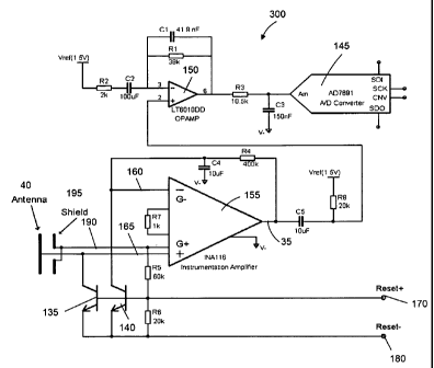
FIG. 4 illustrates one embodiment of the capacitive sensor system of FIG. 1,
including multiple switching devices and a second amplifier for receiving
level
shifted output of the first amplifier. FIG. 4 is a specific example of the
capacitive
sensor system 300 including specific details such as examples of voltage,
capacitance
and resistance values. Particular implementations may vary from these
exemplary
details and still be contemplated to be within the spirit and scope of the
present
invention. The capacitive sensor system 300 of FIG. 4 includes a sensing plate
40 for
capacitively coupling to the body surface 15, a first amplifier 30, a
secondary
amplifier 150, switching devices 135 and 140, capacitors Cl (41.9 nano farad
(nF)) to
C5 (10 micro farad ( F)), resistors R1 (38 kilo ohm) to R8 (20 kilo ohm),
supply
voltages 175 (1.5 volts) and 185 (1.5 volts) and reset voltage references 170
and 180
and a level-shifter formed by capacitor C5 and resistor R8.
The signal on the body surface 15 (skin) capacitively couples to a metal
plate, for example the sensing plate 40 illustrated in FIGs. 1, 2 and 3. The
sensing plate 40 can be incorporated at the bottom of a printed circuit board
(PCB), which is covered with solder mask for electrical insulation of the
sensing
plate 40 or the whole capacitive sensor system 300. A first amplification of
the
signal is accomplished by the first amplifier 30. In one embodiment, the first
amplifier 30 is an instrumentation amplifier, configured for a gain of 50.
Similar
to the capacitive sensor system 10, amplifier 30 is used to amplify the input
signal
received at the input port 25 of the amplifier 30. The input port includes a
negative
amplifier input 160 and a positive amplifier input 165. In some embodiments,
the
instrumentation amplifier 30 may have a low input bias current of 3 femtoamp
(fA)
(typical) and an input current noise of 0.1 fA over (hertz (Hz))-2 (typical).
The capacitive sensor system 300 also features a guard circuit that
incorporates guard pin output or guard output 190, which follows the positive
amplifier input 165 with a gain of 1. Implementation of the guard circuit that
incorporates the guard output 190 is similar to the implementation of the
unity
CA 02706956 2010-05-27
WO 2009/070776 PCT/US2008/085051
-10-
gain amplifier 50 of FIG. 2. In one embodiment, the capacitive sensor system
300
implements a positive guard (for example, positive guard output 190) to
support a
guard ring around the positive amplifier input 165. The positive guard can
also be
used to drive a shielding metal plate 195 associated with the sensing plate
40, where
the shielding metal plate 195 is configured to minimize electric field pick up
from
sources other than the body surface 15, (for example, the scalp). The
shielding
metal plate 195 may be implemented as an inner layer of metal on the printed
circuit board (PCB) above the sensing plate 40. Because the guard circuit that
incorporates the guard output 190 is actively driven to duplicate the voltage
at the
input port 25 of the amplifier 30, it avoids parasitic capacitance division of
signal
gain.
As previously described the reset or switching circuit may be used to prevent
the input bias current of the amplifier from driving the positive amplifier
input 165
toward one of the supply rails of the amplifier 30. The switching or reset
circuit may
include switching devices 135 and 140, resistors R5 (60 kilo ohms) and R6 (20
kilo
ohms) and reset voltage references 170 and 180. The switching devices 135 and
140
(for example, transistors) are turned on by an external circuit including the
reset
voltage references 170 and 180, for example, when the voltage at the input
port 25 is
within the range of voltages included in the input common-mode voltage range
of the
amplifier 30. When the transistors 135 and 140 are off or are not driven, the
base and
emitter nodes, for example, of the transistors 135 and 140 are pulled up by
the guard
output 190. Pulling up the base and emitter nodes of the transistors 135 and
140 by
the guard output 190 is done to minimize leakage currents (and especially the
resultant current noise) from the transistors 135 and 140. The negative
amplifier
input 160 may be made to track the slowly changing positive input with the
feedback
loop consisting of resistor R4 (80 kilo-ohms) and capacitor C4 (100 micro-
farad). This loop also serves to cut off input signals of frequencies below 1
Hz.
At the output port 35, the output of the instrumentation amplifier 30 is level-
shifted and sent to the secondary amplifier 150. The secondary amplifier
150 can be an operational amplifier. A level-shifter is formed by capacitor C5
and resistor R8. This is a common high-pass filter which replaces the low
frequency
CA 02706956 2010-05-27
WO 2009/070776 PCT/US2008/085051
-11-
voltage of the amplifier output port 35 with the voltage Vref (1.5V). The
higher
frequency components of output port 35 pass through the level-shifter
unaffected.
This secondary amplifier 150 can be configured for a gain of 20, for example.
The secondary amplifier 150 includes a second output port 6 and a second input
port
having a second negative input 3 and a second positive input 2. The second
positive
input 2 configured to receive the level shifted output of the instrumentation
amplifier.
A capacitor C2 (100 micro farad) is implemented at the second negative input 3
such that a zero is inserted at 1 Hz by C2, for example, to further cut off
input
signals of frequencies below 1 Hz. Two poles are implemented at 100 Hz by Cl
(41.9 nano farad) reacting with R1 (38 kilo ohm) and C3 (150 nano farad)
reacting with R3 (10.5 kilo ohm). This combination of capacitors and resistors
complete a bandpass filter characteristic between 1 Hz and 100 Hz. Poles and
zeros
are properties of a transfer function representing the input signal for
implementing a
filter. In one embodiment, an analog to digital converter 145 is coupled to
the
secondary amplifier 150 via an interface, for example. The analog to digital
converter
145 receives a secondary amplifier output signal that has been filtered by the
bandpass filter implemented on the secondary amplifier 150. The analog to
digital
converter 145 is, for example, an 18 bit analog to digital converter that
converts the
secondary amplifier output signal to a stream of digital bits. The interface
may
optionally be daisy chained with other analog to digital converters 145 to
reduce the
number of wires in one or more capacitive sensor systems. The output of the
analog
to digital converter is connected to a data acquisition card on user interface
such as a
computer for display on a monitor or to a printer to produce a printed record
of the
measurement device for, for example, for device characterization.
In other embodiment, the total current required for the amplifier 30 is 1 ma
from (a supply rail of) + 5 volts (V) and -5 V power supplies. The secondary
amplifier
150 and the analog to digital converter 145 may use single ended 3V supply and
require 160 microamps total current. In some embodiments, the total power for
the
capacitive sensor system 300 is 10.5 milliwatt, which means that a hundred
capacitive
sensor systems can run for hours on a battery pack.
CA 02706956 2010-05-27
WO 2009/070776 PCT/US2008/085051
-12-
In addition to the examples described above, there are many other ways to
implement a switching circuit that resets that critical sensing node 12. For
example,
the switches themselves can be transistors (bipolar, MOSFET, JFET, MESFET,
etc.),
relays (including traditional relays and micro-mechanical (MEMS) relays,
mechanical
switches, electronics switches, etc.) There may be as few as one switching
device, or
several switching devices. The reference voltages can be set to the middle of
the
amplifier CMR, the supply voltages, or other values. The reference voltages
themselves can be varied by a feedback loop that searches for an optimal
value. The
switching can be performed when the input voltage or the voltage at the
sensing node
12 is deemed close to the limits of the CMR, or at a regular interval. In
either case, a
controller can be used to determine which switching devices to activate, when
to
activate them, and the duration of activation. Alternatively, a human
controller can
determine when to reset the sensing node 12.
In the exemplary embodiment, the capacitive sensor is constructed from two
custom printed circuit boards (PCBs) that are stacked one upon the other. The
upper PCB, which is circular and about the size of a U.S. dime (-18 mm)
includes the secondary amplifier 150, analog to digital converter 145 and some
passive components (for example resistors R1, R2, R3 and capacitors Cl, C2,
C3). The bottom PCB, which is also circular and about the size of a U.S.
quarter (-30
mm), holds the sensing plate 15, shielding plate 195, instrumentation
amplifier 155
and switching devices 135 and 140 (e.g., transistors). In one embodiment, the
bottom layer of the PCB is all metal covered with solder mask. In an
alternative
embodiment, all or a portion of the discrete components on the upper PCB can
be
incorporated into one or more integrated circuits which can be mounted
directly on
top of the lower PCB.
FIGs. 5A and 5B show exemplary results of the effect of the separation
distance between the sensing plate and the body surface on the input signal
gain.
FIG. 5A and FIG. 5B are described with reference to FIGs. 1, 2, 3 and 4. FIG.
5A
shows the measured gain of the input signal over a range of frequencies. The
input signal is the signal generated by the sensing node 12 and received at
the
input port 25 of amplifier 30 or 155. The bandpass characteristic of the
filtering
CA 02706956 2010-05-27
WO 2009/070776 PCT/US2008/085051
-13-
between 1 Hz and 100 Hz as described with respect to FIG. 4 is evident in FIG.
5A.
The 1 Hz cutoff may be steeper since there are three zeros acting there caused
by the
feedback loop of the instrumentation amplifier 155, capacitor C2 in the
secondary
amplifier 150 feedback, and the level-shifter formed by the capacitor C5 and
the
resistor R8. The two poles discussed previously with respect to FIG. 4 act at
a
frequency of 100 Hz.
In one embodiment, the input generated by the sensing node 12, for example
the EEG input, can be modeled as a voltage source coupled into the capacitive
sensor
system 300 through a capacitor. The capacitance can be calculated as the area
of the sensing plate 40 divided by the distance between the sensing plate 40
and the body surface 15 such as the scalp. Since there is also parasitic
capacitance on the positive amplifier input 165 of the instrumentation
amplifier 155
a capacitive voltage divider can be formed at the positive amplifier input 165
which reduces the input signal strength. FIG. 5B shows the gain for three
different
distances between the signal generator, for example the body surface and the
sensing plate 40. As the distance is increased, the input coupling capacitance
is
reduced, as is the overall gain of the circuit. At a distance of 0.2mm, the
gain is
869, whereas it is 539 at 1.6mm and 391 at 3.2mm. The reduction in gain with
distance is significantly larger when the active shield 195 is replaced with a
passive ground shield. With active shield 195, the capacitive sensor system
300,
(e.g., EEG/ECG sensor) is capable of operating over a wide range of
separations as
encountered with typical hair and clothing between the sensing plate 40 and
body
surface 15.
FIGs. 6A and FIG. 6B are sample results illustrating the effect of sensor
separation distance on input referred noise. FIG. 6A and FIG. 6B are described
with
reference to FIGs. 1, 2, 3 and 4. EEG sensor design such as the capacitive
sensor
system 300 requires an amplifier circuit with very low noise. The input
signals
being measured can be as low as tens of microvolts peak-to-peak so noise
levels
below this are desirable. In some embodiments, the analog to digital converter
145 is
not a significant source of noise since it converts a signal that has already
seen a
large gain (gain of 50 at the amplifier 155 and a gain of 20 at the secondary
CA 02706956 2010-05-27
WO 2009/070776 PCT/US2008/085051
-14-
amplifier 150, for example) and it converts at 18-bit levels. The secondary
amplifier 150 also does not contribute significant noise since it comes after
the initial
gain of 50 from the amplifier 155. In one embodiment, the calculated referred-
to-
input (RTI) voltage noise of the amplifier 155 in the frequency band from 1 to
100
Hz is about 0.66 micro volt root mean square ( Vrms. The RTI current noise of
the instrumentation amplifier 155, though extremely small, is integrated by
the
capacitance seen at the positive amplifier input 165. Assuming a distance of
0.2mm
between the sensing plate 40 and the body surface 15, this current noise is
converted to about 1 [tVrms. In one embodiment, capacitive sensor system 300
features a circuit that incorporates guard pin output a guard output 190 and a
guard
input (not shown). Ideally, the guard input keeps the terminals of the
switching
devices 135 and 140 at the same voltage, keeping their leakage noise currents
near zero. The resistor R4, though large, produces thermal noise that is not a
significant factor because it is reduced by the feedback loop implemented on
the
amplifier 155. Thus, the total the expected RTI voltage noise is under 2.0
[tVrms.
The measured noise density as a function of frequency is shown in FIG. 6A.
With
the sensing plate 40 that generates the input signal grounded, a spectral
density
estimate was measured at the output port of the amplifier 150 for distances
between
the sensing plate 40 and the body surface of 0.2 mm, 1.6 mm, and 3.2mm. This
resulted in a measured noise of 1.88 [tVrms. The noise measured at the output
port
of amplifier 150 is then divided by the measured midband gain in FIG. 5A of
the two
amplifiers (for example, 794 or 58 dB). This process of referring the noise to
the
input (RTI) is done in order to compare the magnitude of the noise with the
magnitude of the input signal of interest. The total noise in the frequency
range of
interest, 1-100 Hz, can be obtained by integrating the noise content shown in
FIG. 6A
within this range. FIG. 6B illustrates the results of this calculation for the
three
distances. FIG. 6B also shows the theoretically calculated noise using
estimates of
the noise contributed from the various elements in the circuit. For the
distance of 0.2
mm between sensing plate 40 and the body surface 15, the measured total noise
is
1.88 ilVrms. As the separation distance between the sensing plate 40 and the
body
CA 02706956 2010-05-27
WO 2009/070776 PCT/US2008/085051
-15-
surface 15 increases, the coupling capacitance decreases. The current noise is
then
integrated to a larger voltage noise value.
The current noise is then integrated to a larger voltage noise value. FIG. 6B
illustrates the theoretically calculated noise along with measurements at the
same
three distances used for the gain measurements of FIG. 6A. The input-referred
rms
noise is measured over the 1-100Hz frequency band for the three separation
distances, and compared with the theoretically expected noise. The theoretical
curve accounts for the amplifier's 155 current and voltage input-referred
noise, and for
the capacitive division at the input port 25 of the amplifier 155.
FIG. 7 is a graph of a power spectral density of input signals measured from
two locations of a test subject's head during testing of a prototype
constructed
according to the present invention. In one embodiment, sensing plates 40 are
pressed against the subject's head using a headband, for example. The first
sensing
plate 40 is located in the back of the head (on top of the hair), while the
second was
located behind the ear to be used as a reference. The voltage difference
between
the two sensors was recorded as the subject first closed his eyes for 12
seconds
then kept them open for the same amount of time. The power spectral densities
of the
data from these two blocks of time are shown in FIG. 7. Increased power in the
alpha band of frequencies around 10 Hz can clearly be seen when the eyes are
closed, as is commonly observed in EEG experiments, for example.
FIG. 8 is a record of sample ECG voltage measured through a subject's T-
shirt using sensors constructed according to the present invention. The graph
illustrates the potential difference between two sensing plates 40 positioned
near
the heart. One of the sensing plates was located on top of the chest over the
heart
area and the second sensing plate was located on the side of the chest for use
as a
reference. Both sensing plates 40 were placed outside the subject's t-shirt.
FIG. 8
is a 4 second record, which may be displayed on either or both of a monitor
and a printer.
FIG. 9 illustrates one example of a method of measuring an electric field body
surface using a capacitive sensor system according to an embodiment. The
method
can be implemented in the capacitive sensor system 100, 200 or 300 of FIGs. 2,
3 and
CA 02706956 2010-05-27
WO 2009/070776 PCT/US2008/085051
-16-
4. At block 400 the process starts with capacitively coupling a sensing plate
40 to a
body surface 15. The change in electric potential on the body surface 15
generates an
electric field that induces a change in the electric potential of the sensing
plate 40. The
sensing plate 40 is not in contact with the body surface 15. At block 405 an
input
signal is generated at a sensing node 12 associated with the sensing plate 40.
The
generated input signal is based on the change in the electrical potential of
the sensing
plate 40 where the sensing node 12 is position in the electric field. The
process then
continues to block 410 where the input signal is amplified by an amplifier
having an
input port and an output port. The amplifier is configured to receive the
input signal at
the input port and to generate an output signal at the output port where the
output
signal is based on the amplification of the input signal. Finally, at block
415, a
shunting path is non-continuously closed, using a switching circuit, to reset
the
sensing node that is connected to the input port, wherein the switching
circuit is
connected to the input port and a reference voltage.
The systems and methods described above can be used for measurement of
electroencephalographic (EEG) signals generated by the brain, for use in brain-
computer interfaces. The
systems and methods can also be used in the
electrocardiography (ECG), for heart monitoring, and in electromyography
(EMG),
for recording of muscle activity. Unlike the majority of other EEG/ECG/EMG
sensor
designs, the capacitive sensor system and method described above is capacitive
in
nature and, hence, does not require physical or ohmic contact to the body
surface such
as the skin. Most of the existing sensors require electrical contact to the
skin by
application of conductive gel and/or by abrasive skin preparation, both of
which are
avoided in the present invention.
The capacitive sensor system and methods can be implemented in EEG caps
such as medical diagnostic equipment, neuroprostheses, biofeedback,
neuroimaging,
brain-computer interfaces, and interactive computer games. The capacitive
sensor
system and method can be useful in EEG sensor interfaces to computer game
software
and for industrial applications such as monitoring of electrostatic build-up
in
electronics manufacturing.
CA 02706956 2010-05-27
WO 2009/070776 PCT/US2008/085051
-17-
The embodiments described herein accomplish the above features while
contributing as little noise as possible to the sensing node 12. Only for the
short
duration of time that the switching devices are activated is any noise
contributed.
Furthermore, the switched operation allows replacement of the high resistance
value
with significantly lower resistance values, thus contributing lower thermal
noise
spectral density during activation.
The various embodiments described herein provide a means for combating the
unwanted current at the critical input port of the amplifier with switching
circuitry
that occasionally resets or shunts the sensing node. As described above, the
switching
nature of the inventive circuits offers the advantage that less circuit noise
is injected
into the critical sensing node in a low power circuit.
Those of skill in the art will appreciate that the various illustrative
modules
and method steps described in connection with the above described figures and
the
embodiments disclosed herein can often be implemented as electronic hardware,
software, firmware or combinations of the foregoing. To clearly illustrate
this
interchangeability of hardware and software, various illustrative modules and
method
steps have been described above generally in terms of their functionality.
Whether
such functionality is implemented as hardware or software depends upon the
particular application and design constraints imposed on the overall system.
Skilled
persons can implement the described functionality in varying ways for each
particular
application, but such implementation decisions should not be interpreted as
causing a
departure from the scope of the invention. In addition, the grouping of
functions
within a module or step is for ease of description. Specific functions can be
moved
from one module or step to another without departing from the invention.
Moreover, the various illustrative modules and method steps described in
connection with the embodiments disclosed herein can be implemented or
performed
with hardware such as a general purpose processor, a digital signal processor
("DSP"), an application specific integrated circuit ("ASIC"), field
programmable gate
array ("FPGA") or other programmable logic device, discrete gate or transistor
logic,
discrete hardware components, or any combination thereof designed to perform
the
functions described herein. A general-purpose processor is hardware and can be
a
CA 02706956 2015-02-09
- 18 -
microprocessor, but in the alternative, the processor can be any hardware
processor or
controller, microcontroller. A processor can also be implemented as a
combination of
computing devices, for example, a combination of a DSP and a microprocessor, a
plurality of
microprocessors, one or more microprocessors in conjunction with a DSP core,
or any other
such configuration.
Additionally, the steps of a method or algorithm described in connection with
the
embodiments disclosed herein can be embodied directly in hardware, in a
software module
executed by a processor, or in a combination of the two. A software module can
reside in
computer or controller accessible on readable media including RAM memory,
flash memory,
ROM memory, EPROM memory, EEPROM memory, registers, hard disk, a removable
disk,
a CD-ROM, or any other form of storage medium including a network storage
medium. An
exemplary storage medium can be coupled to the processor so that the processor
can read
information from, and write information to, the storage medium. In the
alternative, the
storage medium can be integral to the processor. The processor and the storage
medium can
also reside in an ASIC.
The scope of the claims should not be limited by the preferred embodiments set
forth
in the examples, but should be given the broadest interpretation consistent
with the
description as a whole.
References
The teachings of the following references provide general background
information.
CA 02706956 2010-05-27
WO 2009/070776 PCT/US2008/085051
-19-
[1] J. C. Chiou, Li-Wei Ko, Chin-Teng Lin, Chao-Ting Hong, Tzyy-Ping Jung,
"Using Novel MEMS EEG Sensors in Detecting Drowsiness Application," IEEE
Biomedical Circuits and Systems Conference, 2006.
[2] A. Lopez and P. C. Richardson, "Capacitive electrocardiographic and
bioelectric
electrodes", IEEE Transactions on Biomedical Engineering, vol. 16, pg. 99,
1969.
[3] T. Matsuo, K. Iinuma, and M. Esashi, "A barium-titanate-ceramics
capacitive-
type EEG electrode", IEEE Transactions on Biomedical Engineering, vol. 188,
pgs 299-300.
[4] R. J. Prance, A. Debray, T. D. Clark, H. Prance, M. Nock, C. J. Harland,
and A. J.
Clippingdale, "An ultra-low-noise electrical-potential probe for human-body
scanning", Measurement Science and Technology, vol. 11, pgs. 291-297, 2000.
[5] C. J. Harland, T. D. Clark and R. J. Prance, "Electric potential
probes¨new
directions in the remote sensing of the human body", Measurement Science and
Technology, vol. 13, pgs. 163-169, 2002.
[6] R. Matthews, N. J. McDonald, I. Fridman, P, Hervieux, and T. Nielsen, "The
invisible electrode ¨ zero prep time, ultra low capacitive sensing. In
Proceedings
of the 1 lth International Conference on Human-Computer Interaction, July 22-
27
2005.
[7] C. Park, P. H. Chou, Y. Bai, R. Matthews, and A. Hibbs, "An ultra-
wearable,
wireless, low power ECG monitoring system", IEEE Biomedical Circuits and
Systems Conference, 2006.
[8] J. Errera and H. S. Sack, "Dielectric properties of animal fibers"
[9] T. Sullivan, S. Deiss, T.P. Jung, and G. Cauwenberghs, "A Low-Noise, Low-
Power EEG Acquisition Node for Scalable Brain-Machine Interfaces", In
Proceedings of the SPIE Conference on Bioengineered and Bioinspired Systems
III, May 2-4 2007.