Note: Descriptions are shown in the official language in which they were submitted.
CA 02707145 2010-05-28
WO 2009/068887
PCT/GB2008/003969
GAS ELECTRON MULTIPLIER DETECTOR
The present invention relates to a Gas Electron Multiplier
ion detector which is used in the detector system of a mass
spectrometer or ion mobility spectrometer. The present invention
also relates to a method of detecting ions and a method of mass
spectrometry.
Gaseous avalanche electron multipliers for the detection of
ionising radiation are known and are often referred to as Gas
Electron Multipliers ("GEM") detectors. Gas Electron Multiplier
detectors represent a significant improvement over conventional
detectors such as multi-wire proportional counters and micro-
patterned detectors. One advantage of known Gas Electron
Multiplier detectors is that they can be moulded into different
shapes. Spatial information can also easily be obtained. Multiple
stages can also be stacked together to produce a low cost detector
which has a significantly increased gain.
It is known to use Gas Electron Multipliers in what is
commonly referred to as a triple GEM configuration. The detector
is used in high energy physics experiments including high energy
particle radiation detection and tracking at moderate (sub-mm)
resolutions. Gas Electron Multipliers may also be used in single-
photon imaging such as in Ring Imaging Cherenkov ("RICH")
detectors. It is also known to use Gas Electron Multiplier ion
detectors in moderate-resolution, beta, gamma-ray, x-ray,
synchrotron and neutron imaging. A further application for Gas
Electron Multipliers is in two-phase and high-pressure cryogenic
detectors for solar neutrino and coherent neutrino scattering
experiments. A yet further use df Gas Electron Multipliers is in
Time Projection Chambers ("TPC").
Gas Electron Multiplier detectors have not been used to
detect low energy ions, since low energy positive ions are repelled
from the entrance to the Gas Electron Multiplier device and hence
are not detected. In analytical instrumentation the majority of
analyte ions of interest are positively charged and hence it is
desired to have instrumentation for the analysis and detection of
analyte ions which is able to detect low energy positive ions.
It is known to use an ion mobility spectrometer to detect and
identify low concentrations of chemicals based upon the
differential migration of gas phase ions through a homogeneous
electric field. Ion mobility spectrometers have become a routine
tool for the field detection of explosives, drugs and chemical
weapons and have found utility as a research tool where they have
an increasing role in the analysis of biologital materials, in
CA 02707145 2010-05-28
W02009/068887
PCT/GB2008/003969
- 2 -
particular in proteomics and metabolomics. Various different forms
of ion mobility spectrometers are known which may be operated under
a range of operating conditions. Ion mobility spectrometers are
often operated at pressures ranging from atmospheric pressure down
to a few tenths of a milli-bar. A Faraday cup or Faraday plate
detector is commonly used as the detector within an ion mobility
spectrometer since Faraday cup or Faraday plate detectors are one
of the few forms of ion detector which are capable of operating at
relatively high sub-atmospheric pressures. By way of contrast, ion
detectors as used in a Time of Flight mass spectrometer require a
high vacuum.
It is known to couple an ion mobility spectrometer with a
mass spectrometer (MS) so that ions are firstly separated according
to their ion mobility and are then mass analysed and detected by
the mass spectrometer or mass analyser. The detection systems
typically utilised in conventional mass spectrometers have a large
gain in order to detect single ion events and typically require
high vacuum (low pressure) e.g. of the order of 10-5 mbar or lower.
Examples of known ion detectors as used in mass spectrometry
instrumentation include electron multiplier (e.g. multi channel
plate and single channel channeltron) detectors, conversion dynodes
with a scintillator or phosphor, and photon multipliers.
The detectors employed in mass spectrometry instrumentation
are capable of detecting a single ion. However, conventional
Faraday cup detectors whether used at high pressure with an ion
mobility spectrometer or used at high vacuum in a mass spectrometer
typically require a minimum of 1000 ions in well shielded static or
immobile instrumentation. Approximately 104 or more ions are
required for handheld or portable instruments. This is mainly, a
consequence of the electronic noise, in particular the Johnson
noise associated with high value resistors, and the lack of any
noise free electronic amplifiers to detect the ion signal.
Faraday cup detectors also typically have a relatively slow
response time due to the use of high value resistors and
unavoidable capacitance in the system.
It is desired to provide an improved ion detector for use
with an ion mobility spectrometer or mass spectrometer.
According to an aspect of the present invention there is
provided a mass spectrometer comprising a Gas Electron Multiplier
ion detector.
The mass spectrometer preferably comprises a device arranged
and adapted either:
(a) to maintain the ion detector at a pressure selected from
CA 02707145 2010-05-28
WO 2009/068887
PCT/GB2008/003969
- 3 -
the group consisting of: (i) < 1000 mbar; (ii) < 100 mbar; (iii) <
mbar; (iv) < 1 mbar; (v) < 0.1 mbar; (vi) < 0.01 mbar; (vii) <
0.001 mbar; (viii) < 0.0001 mbar; and (ix) < 0.00001 mbar; and/or
(b) to maintain the ion detector in a mode of operation at a
pressure selected from the group consisting of: (i) > 1000 mbar;
(ii) > 100 mbar; (iii) > 10 mbar; (iv) > 1 mbar; (v) > 0.1 mbar;
(vi) > 0.01 mbar; (vii) > 0.001 mbar; and (viii) > 0.0001 mbar
and/or
(c) to maintain the ion detector in a mode of operation at a
pressure selected from the group consisting of: (i) 0.0001-0.001
mbar; (ii) 0.001-0.01 mbar; (iii) 0.01-0.1 mbar; (iv) 0.1-1 mbar;
(v) 1-10 mbar; (vi) 10-100 mbar; and (vii) 100-1000 mbar.
The ion detector is preferably arranged and adapted to detect
ions having an energy selected from the group consisting of: (i) <
1 eV; (ii) 1-5 eV; (iii) 5-10 eV; (iv) 10-15 eV; (v) 15-20 eV; (vi)
20-25 eV; (vii) 25-30 eV; (viii) 30-35 eV; (ix) 35-40 eV; (x) 40-45
eV; (xi) 45-50 eV; (xii) 50-55 eV; (xiii) 55-60 eV; (xiv) 60-65 eV;
(xv) 65-70 eV; (xvi) 70-75 eV; (xvii) 75-80 eV; (xviii) 80-85 eV;
(xix) 85-90 eV; (xx) 90-95 eV; (xxi) 95-100 eV; (xxii) 100-105 eV;
(xxiii) 105-110 eV; (xxiv) 110-115 eV; (xxv) 115-120 eV; (xxvi)
120-125 eV; (xxvii) 125-130 eV; (xxviii) 130-135 eV; (xxix) 135-140
eV; (xxx) 140-145 eV; (xxxi) 145-150 eV; (xxxii) 150-155 eV;
(xxxiii) 155-160 eV; (xxxiv) 160-165 eV; (xxxv) 165-170 eV; (xxxvi)
170-175 eV; (xxxvii) 175-180 eV; (xxxviii) 180-185 eV; (xxxix) 185-
190 eV; (xl) 190-195 eV; (xli) 195-200 eV; and (xlii) > 200 eV. It
will be apparent that the preferred ion detector is arranged and
adapted to detect ions having a significantly lower energy that
conventional radiation detectors which may be arranged to detect
particles having energies in the range key to Hey.
The ion detector preferably comprises a first foil layer, a
first substrate or a first gas electron multiplier stage.
According to an embodiment 0-5%, 5-10%, 10-15%, 15-20%, 20-25%, 25-
.30%, 30-35%, 35-40%, 40-45%, 45-50%, 50-55%, 55-60%, 60-65%, 65-
70%, 70-75%, 75-80%, 80-85%, 85-90%, 90-95% or 95-100% of an upper
and/or lower surface of the first foil layer, the first substrate
or the first gas electron multiplier stage may comprise a first
surface layer or coating which is either:
(i) arranged and adapted to enhance the yield of secondary
ions and/or electrons; and/or
(ii) a photocathode layer which is arranged and adapted to
receive photons and to release photoelectrons.
The ion detector preferably comprises a second foil layer, a
second substrate or a second gas electron multiplier stage.
CA 02707145 2010-05-28
WO 2009/068887
PCT/GB2008/003969
- 4 -
According to an embodiment 0-5%, 5-10%, 10-15%, 15-20%, 20-25%, 25-
30%, 30-35%, 35-40%, 40-45%, 45-50%, 50-55%, 55-60%, 60-65%, 65-
70%, 70-75%, 75-80%, 80-85%, 85-90%, 90-95% or 95-100% of an upper
and/or lower surface of the second foil layer, the second substrate
or the second gas electron multiplier stage may comprise a second
surface layer or coating which is either:
(i) arranged and adapted to enhance the yield of secondary
ions and/or electrons; and/or
(ii) a photocathode layer which is arranged and adapted to
receive photons and to release photoelectrons.
The ion detector preferably comprises a third foil layer, a
third substrate, or a third gas electron multiplier stage.
According to an embodiment 0-5%, 5-10%, 10-15%, 15-20%, 20-25%, 25-
30%, 30-35%, 35-40%, 40-45%, 45-50%, 50-55%, 55-60%, 60-65%, 65-
70%, 70-75%, 75-80%, 80-85%, 85-90%, 90-95% or 95-100% of an upper
and/or lower surface of the third foil layer, the third substrate
or the third gas electron multiplier stage may comprise a third
surface layer or coating which is either:
(i) arranged and adapted to enhance the yield of secondary
ions and/or electrons; and/or
(ii) a photocathode layer which is arranged and adapted to
receive photons and to release photoelectrons.
The ion detector preferably comprises a fourth foil layer, a
fourth substrate or a fourth gas electron multiplier stage.
According to an embodiment 0-5%, 5-10%, 10-15%, 15-20%, 20-25%, 25-
30%, 30-35%, 35-40%, 40-45%, 45-50%, 50-55%, 55-60%, 60-65%, 65-
70%, 70-75%, 75-80%, 80-85%, 85-90%, 90-95% or 95-100% of an upper
and/or lower surface of the fourth foil layer, the fourth substrate
or the fourth gas electron multiplier stage may comprise a fourth
surface layer or coating which is either:
(i) arranged and adapted to enhance the yield of secondary
ions and/or electrons; and/or
(ii) a photocathode layer which is arranged and adapted to
receive photons and to release photoelectrons.
The first surface layer or coating and/or the second surface
layer or coating and/or the third surface layer or coating and/or
the fourth surface layer or coating is preferably selected from the
group consisting of: (i) caesium iodide (CsI); (ii) caesium
telluride (CsTe); (iii) aCH:N, amorphous carbon or Diamond Like
Carbon ("DLC"); (iv) copper; (v) aluminium; (vi) magnesium oxide
(MgO); (vii) magnesium fluoride (MgF2); and (viii) tungsten.
According to an embodiment the first foil layer, the first
substrate or the first gas electron multiplier stage and/or the
CA 02707145 2010-05-28
WO 2009/068887
PCT/GB2008/003969
- 5 --
second foil layer, the second substrate or the second gas electron
multiplier stage and/or the third foil layer, the third substrate
or the third gas electron multiplier stage and/or the fourth foil
layer, the fourth substrate or the fourth gas electron multiplier
stage are preferably fabricated from a material selected from the
group consisting of: (i) Kapton (RTM); (ii)
Polytetrafluoroethylene; (iii) a ceramic; (iv) a glass; (v) a
plastics material; (vi) an insulating material; and (vii) a polymer
sheet. The foil layers may also be made from the same materials
which are used to manufacture printed circuit boards.
According to an embodiment the first foil layer, the first
substrate or the first gas electron multiplier stage and/or the
second foil layer, the second substrate or the second gas electron
multiplier stage and/or the third foil layer, the third substrate
or the third gas electron multiplier stage and/or the fourth foil
layer, the fourth substrate or the fourth gas electron multiplier
stage preferably have a thickness selected from the group
consisting of: (i) < 1 pm; (ii) 1-5 pm; (iii) 5-10 pm; (iv) 10-15
pm; (v) 15-20 pm; (vi) 20-25 pm; (vii) 25-30 pm; (viii) 30-35 pm;
(ix) 35-40 pm; (x) 40-45 pm; (xi) 45-50 pm; (xii) 50-55 pm; (xiii)
55-60 pm; (xiv) 60-65 pm; (xv) 65-70 pm; (xvi) 70-75 pm; (xvii) 75-
80 pm; (xviii) 80-85 pm; (xix) 85-90 pm; (xx) 90-95 pm; (xxi) 95-
100 pm; (xxii) 100-200 pm; (xxiii) 200-300 pm; (xxiv) 300-400 pm;
(xxv) 400-500 pm; (xxvi) 500-600 pm; (xxvii) 600-700 pm; (xxviii)
700-800 pm; (xxix) 800-900. pm; (xxx) 900-1000 pm; (xxxi) 1-2 mm;
(xxxii) 2-3 mm; (xxxiii) 3-4 mm; (xxxiv) 4-5 mm; and (xxxv) > 5 mm.
Although the preferred thickness of the foil layers is
approximately 50 pm, according to an alternative embodiment a
relatively thick (e.g. 1 mm) substrate layer may be provided in at
least one of the Gas Electron Multiplier stages.
,According to an embodiment the first foil layer, the first
substrate or the first gas electron multiplier stage and/or the
second foil layer, the second substrate or the second gas electron
multiplier stage and/or the third foil layer, the third substrate
or the third gas electron multiplier stage and/or the fourth foil
layer, the fourth substrate or the fourth gas electron multiplier
stage are preferably coated on an upper and/or lower surface with a
copper or other metallic or conductive coating or layer.
According to an embodiment the first foil layer, the first
substrate or the first gas electron multiplier stage and/or the
second foil layer, the second substrate or the second gas electron
multiplier stage and/or the third foil layer, the third substrate
or the third gas electron multiplier stage and/or the fourth foil
CA 02707145 2010-05-28
WO 2009/068887
PCT/GB2008/003969
- 6 -
layer , the fourth substrate or the fourth gas electron multiplier
stage are preferably coated on an upper and/or lower surface with a
copper or other metallic or conductive coating having a thickness
selected from the group consisting of: (i) < 1 pm; (ii) 1-5 pm;
(iii) 5-10 pm; (iv) 10-15 pm; (v) 15-20 pm; (vi) 20-25 pm; (vii)
25-30 pm; (viii) 30-35 pm; (ix) 35-40 pm; (x) 40-45 pm; (xi) 45-50
pm; and (xii) > 50 pm.
According to an embodiment the first foil layer, the first
substrate or the first gas electron multiplier stage and/or the
second foil layer, the second substrate or the second gas electron
multiplier stage and/or the third foil layer, the third substrate
=or the third gas electron multiplier stage and/or the fourth foil
layer, the fourth substrate or the fourth gas electron multiplier
stage preferably comprise a plurality of holes having a maximum
and/or minimum diameter selected from the group consisting of: (i)
< 1 pm; (ii) 1-5 pm; (iii) 5-10 pm; (iv) 10-15 pm; (v) 15-20 pm;
(vi) 20-25 pm; (vii) 25-30 pm; (viii) 30-35 pm; (ix) 35-40 pm; (x)
40-45 pm; (xi) 45-50 pm; (xii) 50-55 pm; (xiii) 55-60 pm; (xiv) 60-
65 pm; (xv) 65-70 pm; (xvi) 70-75 pm; (xvii) 75-80 pm; (xviii) 80-
85 pm; (xix) 85-90 pm; (xx) 90-95 pm; (xxi) 95-100 pm; and (xxii) >
100 pm.
The first foil layer, the first substrate or the first gas
electron multiplier stage and/or the second foil layer, the second
substrate or the second gas electron multiplier stage and/or the
third foil layer, the third substrate or the third gas electron
multiplier stage and/or the fourth foil layer, the fourth substrate
or the fourth gas electron multiplier stage preferably comprise a
plurality of holes having a tubular, conical, bi-conical or concave
channel.
The first foil layer, the first substrate or the first gas
electron multiplier stage and/or the second foil layer, the second
substrate or the second gas electron multiplier stage and/or the
third foil layer, the third substrate or the third gas electron
multiplier stage and/or the fourth foil layer, the fourth substrate
or the fourth gas electron multiplier stage preferably comprise a
plurality of holes having a pitch selected from the group
consisting of: (i) < 1 pm; (ii) 1-5 pm; (iii) 5-10 pm; (iv) 10-15
pm; (v) 15-20 pm; (vi) 20-25 pm; (vii) 25-30 pm; (viii) 30-35 pm;
(ix) 35-40 pm; (x) 40-45 pm; (xi) 45-50 pm; (xii) 50-55 pm; (xiii)
55-60 pm; (xiv) 60-65 pm; (xv) 65-70 pm; (xvi) 70-75 pm; (xvii) 75-
80 pm; (xviii) 80-85 pm; (xix) 85-90 pm; (xx) 90-95 pm; (xxi) 95-
100 pm; (xxii) 100-110 pm; (xxiii) 110-120 pm; (xxiv) 120-130 pm;
(xxv) 130-140 pm; (xxvi) 140-150 pm; (xxvii) 150-160 pm; (xxviii)
CA 02707145 2010-05-28
WO 2009/068887 PCT/GB2008/003969
-7-
160-170 pm; (xxix) 170-180 pm; (xxx) 180-190 pm; (xxxi) 190-200 pm;
and (xxxii) > 200 pm.
A voltage or potential difference is preferably maintained
between an upper and lower surface of the first foil layer, the
first substrate or the first gas electron multiplier stage, wherein
the voltage or potential difference is preferably selected from the
group consisting of: (i) < 50 V; (ii) 50-100 V; (iii) 100-150 V;
(iv) 150-200 V; (v) 200-250 V; (vi) 250-300 V; (vii) 300-350 V;
(viii) 350-400 V; (ix) 400-450 V; (x) 450-500 V; (xi) 500-550 V;
(xii) 550-600 V; (xiii) 600-650 V; (xiv) 650-700 V; (xv) 700-750 V;
(xvi) 750-800 V; (xvii) 800-850 V; (xviii) 850-900 V; (xix) 900-950
V; (xx) 950-1000 V; and (xxi) > 1000 V.
A voltage or potential difference is preferably maintained
between an upper and lower surface of the second foil layer, the
second substrate or the second gas electron multiplier stage,
wherein the voltage or potential difference is preferably selected
from the group consisting of: (i) < 50 V; (ii) 50-100 V; (iii) 100-
150 V; (iv) 150-200 V; (v) 200-250 V; (vi) 250-300 V; (vii) 300-350
V; (viii) 350-400 V; (ix) 400-450 V; (x) 450-500 V; (xi) 500-550 V;
(xii) 550-600 V; (xiii) 600-650 V; (xiv) 650-700 V; (xv) 700-750 V;
(xvi) 750-800 V; (xvii) 800-850 V; (xviii) 850-900 V; (xix) 900-950
V; (xx) 950-10,00 V; and (xxi) > 1000 V.
A voltage or potential difference is preferably maintained
between an upper and lower surface of the third foil layer, the
third substrate or the third gas electron multiplier stage, wherein
the voltage or potential difference is preferably selected from the
group consisting of: (i) < 50 V; (ii) 50-100 V; (iii) 100-150 V;
(iv) 150-200 V; (v) 200-250 V; (vi) 250-300 V; (vii) 300-350 V;
(viii) 350-400 V; (ix) 400-450 V; (x) 450-500 V; (xi) 500-550 V;
(xii) 550-600 V; (xiii) 600-650 V; (xiv) 650-700 V; (xv) 700-750 V;
(xvi) 750-800 V; (xvii) 800-850 V; (xviii) 850-900 V; (xix) 900-950
V; (xx) 950-1000 V; and (xxi) > 1000 V.
A voltage or potential difference is preferably maintained
between an upper and lower surface of the fourth foil layer, the
fourth substrate or the fourth gas electron multiplier stage,
wherein the voltage or potential difference is preferably selected
from the group consisting of: (i) < 50 V; (ii) 50-100 V; (iii) 100-
150 V; (iv) 150-200 V; (v) 200-250 V; (vi) 250-300 V; (vii) 300-350
V; (viii) 350-400 V; (ix) 400-450 V; (x) 450-500 V; (xi) 500-550 V;
(xii) 550-600 V; (xiii) 600-650 V; (xiv) 650-700 V; (xv) 700-750 V;
(xvi) 750-800 V; (xvii) 800-850 V; (xviii) 850-900 V; (xix) 900-950
V; (xx) 950-1000 V; and (xxi) > 1000 V.
An electric field is preferably maintained into holes in the
CA 02707145 2010-05-28
WO 2009/068887
PCT/GB2008/003969
- 8 -
f irs t foil layer, the first substrate or the first gas electron
multiplier stage and/or into holes in the second foil layer, the
second substrate or the second gas electron multiplier stage and/or
into holes in the third foil layer, the third substrate or the
third gas electron multiplier .stage and/or into holes in the fourth
foil layer, the fourth substrate or the fourth gas electron
multiplier stage, wherein the electric field is selected from the
group consisting of: (i) < 10 kV/cm; (ii) 10-20 kV/cm; (iii) 20-30
kV/cm; (iv) 30-40 kV/cm; (v) 40-50 kV/cm; (vi) 50-60 kV/cm; (vii)
60-70 kV/cm; (viii) 70-80 kV/cm; (ix) 80-90 kV/cm; (x) 90-100
kV/cm; (xi) 100-150 kV/cm; (xii) 150-200 kV/cm; (xiii) 200-250
kV/cm; (xiv) 250-300 kV/cm; (xv) 300-350 kV/cm; (xvi) 350-400
kV/cm; (xvii) 400-450 kV/cm; (xviii) 450-500 kV/cm; and (xix) > 500
kV/cm.
The centre-to-centre'spacing between the first foil layer,
the first substrate or the first gas electron multiplier stage
and/or the second foil layer, the second substrate or the second
gas electron multiplier stage and/or the third foil layer, the
third substrate or the third gas electron multiplier stage and/or
the fourth foil layer, the fourth substrate or the fourth gas
electron multiplier stage is preferably selected from the group
consisting of: (i) < 0.2 mm; (ii) 0.2-0.4 mm; (iii) 0.4-0.6 mm;
(iv) 0.6-0.8 mm; (v) 0.8-1.0 mm; (vi) 1.0-1.2 mm; (vii) 1.2-1.4 mm;
(viii) 1.4-1.6 mm; (ix) 1.6-1.8 mm; (x) 1.8-2.0 mm; (xi) 2.0-2.2
mm; (xii) 2.2-2.4 mm; (xiii) 2.4-2.6 mm; (xiv) 2.6-2.8 mm; (xv)
2.8-3.0 mm; (xvi) 3.0-3.2 mm; (xvii) 3.2-3.4 mm; (xviii) 3.4-3.6
mm; (xix) 3.6-3.8 mm; 0o0 3.8-4.0 mm; (xxi) 4.0-4.2 mm; (xxii)
4.2-4.4 mm; (xxiii) 4.4-4.6 mm; (xxiv) 4.6-4.8 mm; (xxv) 4.8-5.0
mm; (xxvi) 5.0-6.0 mm; (xxvii) 6.0-7.0 mm; (xxviii) 7.0-8.0 mm;
(xxix) 8.0-9.0 mm; (xxx) 9.0-10.0 mm; and (xxxi) > 10.0 mm.
A charge blocking mesh electrode may be provided between the
first foil layer, the first substrate or the first gas electron
multiplier stage and the second foil layer, the second substrate or
the second gas electron multiplier stage.
A charge blocking mesh electrode may be provided between the
second foil layer, the second substrate or the second gas electron
multiplier stage and the third foil layer, the third substrate or
the third gas electron multiplier stage.
A charge blocking mesh electrode may be provided between the
third foil layer, the third substrate or the third gas electron
multiplier stage and the fourth foil layer, the fourth substrate or
the fourth gas electron multiplier stage.
One or .more anodes and/or one or more cathodes may be
CA 02707145 2010-05-28
WO 2009/068887
PCT/GB2008/003969
- 9 -
provided on an upper and/or lower surface of the first foil layer,
the first substrate or the first gas electron multiplier stage.
One or more anodes and/or one or more cathodes are preferably
provided on an upper and/or lower surface of the second foil layer,
the second substrate or the second gas electron multiplier stage.
One or more anodes and/or one or more cathodes are preferably
provided on an upper and/or lower surface of the third foil layer,
the third substrate or the third gas electron multiplier stage.
One or more anodes and/or one or more cathodes are preferably
provided on an upper and/or lower surface of the fourth foil layer,
=the fourth substrate or the fourth gas electron multiplier stage.
The ion detector preferably comprises one or more electrodes,
counter electrodes or cathodes arranged either:
(i) adjacent and/or facing and/or opposed to the first foil
layer, the first substrate or the first gas electron multiplier
stage; and/or
(ii) in a drift or input region of the ion detector; and/or
(iii) to receive analyte cations and to release secondary
electrons and/or secondary anions and/or secondary cations.
The one or more electrodes, counter electrodes or cathodes
preferably comprise:
(i) one or more planar electrodes; and/or
(ii) one or more grid or mesh electrodes; and/or
(iii) one or more electrodes having one or more apertures
through which ions or analyte cations may be transmitted in use.
According to an embodiment ions may be transmitted through a
grid cathode electrode.
According to an embodiment 0-5%, 5-10%, 10-15%, 15-20%, 20-
25%, 25-30%, 30-35%, 35-40%, 40-45%, 45-50%, 50-55%, 55-60%, 60-
65%, 65-70%, 70-75%, 75-80%, 80-85%, 85-90%, 90-95% or 95-100% of
an upper and/or lower surface of the one or more electrodes,
counter electrodes or cathodes may comprise a surface layer or
coating which is either:
(i) arranged and adapted to enhance the yield of secondary
ions and/or electrons; and/or
(ii) a photocathode layer which is arranged and adapted to
receive photons and to release photoelectrons.
The surface coating is preferably selected from the group
consisting of: (i) caesium iodide (CsI); (ii) caesium telluride
(CsTe); (iii) aCH:N, amorphous carbon or Diamond Like Carbon
("DLC"); (iv) copper; (v) aluminium; (vi) magnesium oxide (MgO);
(vii) magnesium fluoride (MgF2); and (viii) tungsten.
According to an embodiment:
CA 02707145 2010-05-28
WO 2009/068887
PCT/GB2008/003969
- 10 -
( i ) the one or more electrodes, counter electrodes or
cathodes may be maintained, in use, at a negative potential
relative to an upper and/or lower surface of the first foil layer,
the first substrate or the first gas electron multiplier stage;
and/or
(ii) positively charged analyte ions may be accelerated away,
in use, from the first foil layer, the first substrate or the first
gas electron multiplier stage and are accelerated towards the one
or more electrodes, counter electrodes or cathodes; and/or
(iii) positively charged analyte ions may be caused, in use,
to impact the surface of the one or more electrodes, counter
electrodes or cathodes and to yield secondary anions and/or
secondary cations and/or secondary electrons; and/or
(iv) at least some secondary anions and/or secondary cations
and/or secondary electrons are preferably accelerated, in use,
through one or more holes in the first foil layer, the first
substrate or the first gas electron multiplier stage; and/or
(v) at least some secondary anions and/or secondary cations
and/or the secondary electrons emitted from the one or more
electrodes, counter electrodes or cathodes are preferably caused,
in use, to impact the surface of the first foil layer, the first
substrate or .the first gas electron multiplier stage and to yield
further electrons; and/or
(vi) negatively charged analyte ions are preferably caused,
in use, to be accelerated through one or more holes in the first
foil layer, the first substrate or the first gas electron
multiplier stage; and/or
(vii) electrons are preferably directed onto one or more
anodes arranged on an upper and/or lower surface of the first foil
layer, the first substrate or the first gas electron multiplier
stage whereupon a plurality of electrons and/or photons are
produced; and/or
(viii) electrons are preferably directed onto one or more
anodes arranged on an upper and/or lower surface of the second foil
layer, the second substrate or the second gas electron multiplier
stage whereupon a plurality of electrons and/or photons are
produced; and/or
(ix) electrons are preferably directed onto one or more
anodes arranged on an upper and/or lower surface of the third foil
layer, the third substrate or the third gas electron multiplier
stage whereupon a plurality of electrons and/or photons are
produced; and/or
(x) electrons are preferably directed onto one or more anodes
CA 02707145 2010-05-28
W02009/068887
PCT/GB2008/003969
- 11 -
arranged on an upper and/or lower surface of the fourth foil layer,
the fourth substrate or the fourth gas electron multiplier stage
whereupon a plurality of electrons and/or photons are produced;
and/or
(xi) avalanche generated photons are preferably caused to
pass through a charge blocking mesh electrode located between the
first. foil layer, the first substrate or the first gas electron "
multiplier stage and the second foil layer, the second substrate or
the second gas electron multiplier stage; and/or
(xii) avalanche generated photons are preferably caused to
pass through a charge blocking mesh electrode located between the
second foil layer, the second substrate or the second gas electron
multiplier stage and the third foil layer, the third substrate or
the third gas electron multiplier stage; and/or
(xiii) avalanche generated photons are preferably caused to
pass through a charge blocking mesh electrode located between the
third foil layer, the third substrate or the third gas electron
multiplier stage and the fourth foil layer, the fourth substrate or
the fourth gas electron multiplier stage; and/or
(xiv) positively charged analyte ions are preferably caused,
in use, to impact the surface of the one of more electrodes,
counter electrodes or cathodes with a velocity selected from the
group consisting of: (i) < 1 mm/ps; (ii) 1-5 mm/ps; (iii) 5L10
mm/ps; (iv) 10-15 mm/ps; (v) 15-20 mm/ps; (vi) 20-25 mm/ps; (vii)
25-30 mm/ps; (viii) 30-35 mm/ps; (ix) 35-40 mm/ps; (x) 40-45 mm/ps;
(xi) 45-50 mm/ps; (xii) 50-55 mm/ps; (xiii) 55-60 mm/ps; (xiv) 60-
65 mm/ps; (xv) 65-70 mm/ps; (xvi) 70-75 mm/ps; (xvii) 75-80 mm/ps;
(xviii) 80-85 mm/ps; (xix) 85-90 mm/ps; (xx) 90-95 mm/ps; (xxi) 95-
100 mm/ps-; and (xxii) > 100 mm/ps.
The ion detector preferably further comprises:
(i) one or more readout electrodes; and/or
(ii) one or more photo-multiplier tubes ("PMT"); and/or
(iii) one or more charge coupled detectors ("CCD").
The one or more readout electrodes and/or one or more photo-
multiplier tubes ("PMT") and/or one or more charge coupled
detectors ("CCD") are preferably arranged downstream of the last
foil layer, substrate or gas electron multiplier stage and are
preferably arranged to detect electrons and/or photons emitted from
the last foil electrode or Gas Electron Multiplier stage. The one
or more readout electrodes and/or one or more photo-multiplier
tubes ("PMT") and/or one or more charge coupled detectors ("CCD")
are preferably connected to a readout anode and/or readout
electronics.
CA 02707145 2010-05-28
WO 2009/068887 PCT/GB2008/003969
- 12 -
The mass spectrometer preferably further comprises either:
(a) an ion source arranged, wherein the ion source is selected
from the group consisting of: (i) an Electrospray ionisation
("ESI") ion source; (ii) an Atmospheric Pressure Photo Ionisation
("APPI") ion source; (iii) an Atmospheric Pressure Chemical
Ionisation ("APCI") ion source; (iv) a Matrix Assisted Laser
Desorption Ionisation ("MALDI") ion source; (v) a Laser Desorption
Ionisation ("LDI") ion source; (vi) an Atmospheric Pressure
Ionisation ("API") ion source; (vii). a Desorption Ionisation on
Silicon ("DIOS") ion source; (viii) an Electron Impact ("El") ion
source; (ix) a Chemical Ionisation ("CI") ion source; (x) a Field
Ionisation ("Fl") ion source; (xi) a Field Desorption ("FD") ion
source; (xii) an Inductively Coupled Plasma ("ICP") ion source;
(xiii) a Fast Atom Bombardment .("FAB") ion source; (xiv) a Liquid
Secondary Ion Mass Spectrometry ("LSIMS") ion source; (xv) a
Desorption Electrospray Ionisation ("DEBI") ion source; (xvi) a
Nickel-63 radioactive ion source; (xvii) an Atmospheric Pressure
Matrix Assisted Laser Desorption Ionisation ion source; (xviii) a
Thermospray ion source; (xix) an Atmospheric Sampling Glow
Discharge Ionisation ("ASGDI") ion source; and (xx) a Glow
Discharge ("GD") ion source; and/or
(b) one or more continuous or pulsed ion sources; and/or
(c) one or more ion guides; and/or
(d) one or more ion mobility separation devices and/or one or
more Field Asymmetric Ion Mobility Spectrometer devices; and/or
(e) one or more ion traps or one or more ion trapping regions;
and/or
(f) one or more collision, fragmentation or reaction cells,
wherein the one or more collision, fragmentation or reaction cells
are selected from the group consisting of: (i) a Collisional
Induced Dissociation ("CID") fragmentation device; (ii) a Surface
Induced Dissociation ("SID") fragmentation device; (iii) an
Electron Transfer Dissociation ("ETD") fragmentation device; (iv)
an Electron Capture Dissociation ("ECD") fragmentation device; (v)
an Electron Collision or Impact Dissociation fragmentation device;
(vi) a Photo Induced Dissociation ("PID") fragmentation device;
(vii) a Laser Induced Dissociation fragmentation device; (viii) an
infrared radiation induced dissociation device; (ix) an ultraviolet
radiation induced dissociation device; (x) a nozzle-skimmer
interface fragmentation device; (xi) an in-source fragmentation
device; (xii) an in-source Collision Induced Dissociation
fragmentation device; (xiii) a thermal or temperature source
fragmentation device; (xiv) an electric field induced fragmentation
=
CA 02707145 2010-05-28
W02009/068887
PCT/GB2008/003969
- 13 -
device; (xv) a magnetic field induced fragmentation device; (xvi)
an enzyme digestion or enzyme degradation fragmentation device;
(xvii) an ion-ion reaction fragmentation device; (xviii) an ion-
molecule reaction fragmentation device; (xix) an ion-atom reaction
fragmentation device; (xx) an ion-metastable ion reaction
fragmentation device; (xxi) an ion-metastable molecule reaction
fragmentation device; (xxii) an ion-metastable atom reaction
fragmentation device; (xxiii) an ion-ion reaction device for
reacting ions to form adduct or product ions; (xxiv) an ion-
molecule reaction device for reacting ions to form adduct or
product ions; (xxv) an ion-atom reaction device for reacting ions
to form adduct or product ions; (xxvi) an ion-metastable ion
reaction device for reacting ions to form adduct or product ions;
(xxvii) an ion-metastable molecule reaction device for reacting
ions to form adduct or product ions; (xxviii) an ion-metastable
atom reaction device for reacting ions to form adduct or product
ions; and (xxix) an Electron Ionisation Dissociation ("EID")
fragmentation device; and/or
(g) a mass analyser selected from the group consisting of: (i)
a quadrupole mass analyser; (ii) a 2D or linear quadrupole mass
analyser; (iii) a Paul or 3D quadrupole mass analyser; (iv) a
Penning trap mass analyser; (v) an ion trap mass analyser; (vi) a
magnetic sector mass analyser; (vii) a Time of Flight mass
analyser; (viii) an orthogonal acceleration Time of Flight mass
analyser; and (ix) a linear acceleration Time of Flight mass
analyser; and/or
(h) one or more energy analysers or electrostatic energy
analysers; and/or
(i) one or more ion detectors; and/or
(j) one or more mass filters, wherein the one or more mass
filters are selected from the group consisting of: (i) a quadrupole
mass filter; (ii) a 2D or linear quadrupole ion trap; (iii) a Paul
or 3D quadrupole ion trap; (iv) a Penning ion trap; (v) an ion
trap; (vi) a magnetic sector mass filter; (vii) a Time of Flight
mass filter; and (viii) a Wein filter; and/or
(k) a device for converting a substantially continuous ion
beam into a pulsed ion beam.
According to an embodiment the mass spectrometer may
comprise:
a C-trap; and
a mass analyser;
wherein in a first mode of operation ions are transmitted to
the C-trap and are then injected into the mass analyser; and
CA 02707145 2010-05-28
WO 2009/068887
PCT/GB2008/003969
- 14 -
wherein in a second mode of operation ions are transmitted to
the C-trap and then to a collision, fragmentation or reaction cell
or an Electron Transfer Dissociation and/or Proton Transfer
Reaction device wherein at least some ions are fragmented into
fragment ions and/or reacted to form product ions, and wherein the
fragment ions and/or the product ions are then transmitted to the
C-trap before being injected into the mass analyser.
The ion detector preferably has a gain selected from the
group consisting of: (i) < 10; (ii) 10-100; (iii) 100-1000, (iv)
10-l0; (v) 104-105; (vi) 105-106; (vii) 106-107; and (viii) > 107.
According to another aspect of the present invention there is
provided a method of mass spectrometry comprising:
using a Gas Electron Multiplier ion detector to detect ions.
According to another aspect of the present invention there is
provided apparatus comprising:
an ion mobility spectrometer comprising a first plurality of
electrodes and/or an ion fragmentation or reaction device
comprising a second plurality of electrodes; and
a Gas Electron Multiplier ion detector which is arranged and
adapted to detect ions which emerge from the ion mobility
spectrometer and/or from the ion fragmentation or reaction device.
According to an embodiment:
(a) the ion mobility spectrometer is arranged to cause ions
to separate temporally according to their ion mobility; and/or
(b) the ion mobility spectrometer comprises a Field
Asymmetric Ion Mobility Spectrometer ("FAIMS") which is arranged
and adapted to cause ions to separate temporally according to their
rate of change of ion mobility with electric field strength; and/or
(c) in use a buffer, reaction or fragmentation gas is
provided within the ion mobility spectrometer and/or the ion
fragmentation or reaction device; and/or
(d) the ion mobility spectrometer comprises a gas phase
electrophoresis device; and/or
(e) the ion mobility spectrometer comprises a drift tube and
one or more electrodes for maintaining an axial DC voltage gradient
along at least a portion of the drift tube; and/or
(f) the ion mobility spectrometer and/or the ion
fragmentation or reaction device comprises one or more multipole
rod sets; and/or
(g) the ion mobility spectrometer and/or the ion
fragmentation or reaction device comprises one or more quadrupole,
hexapole, octapole or higher order rod sets; and/or
CA 02707145 2010-05-28
WO 2009/068887
PCT/GB2008/003969
- 15 -
( h) the ion mobility spectrometer and/or the ion
fragmentation or reaction device comprises one or more quadrupole,
hexapole, octapole or higher order rod sets, wherein the one or
more multipole rod sets are axially segmented or comprise a
plurality of axial segments; and/or
(i) the ion mobility spectrometer and/or the ion
fragmentation or reaction device comprises at least 5, 10, 15, 20,
25, 30, 35, 40, 45, 50, 55, 60, 65, 70, 75, 80, 85, 90, 95 or 100
electrodes; and/or
(j) at least 5%, 10%, 15%, 20%, 25%, 30%, 35%, 40%, 45%, 50%,
55%, 60%, 65%, 70%, 75%, 80%, 85%, 90%, 95% or 100% of the first
electrodes and/or at least 5%, 10%, 15%, 20%, 25%, 30%, 35%, 40%,
45%, 50%, 55%, 60%, 65%, 70%, 75%, 80%, 85%, 90%, 95% or 100% of
the second electrodes have apertures through which ions are
transmitted in use; and/or
(k) at least 5%, 10%, 15%, 20%, 25%, 30%, 35%, 40%, 45%, 50%,
55%, 60%, 65%, 70%, 75%, 80%, 85%, 90%, 95% or 100% of the first
electrodes and/or at least 5%, 10%, 15%, 20%, 25%, 30%, 35%, 40%,
45%, 50%, 55%, 60%, 65%, 70%, 75%, 80%, 85%, 90%, 95% or 100% of
the second electrodes have apertures which are of substantially the
same size or area; and/or
(1) at least 5%, 10%, 15%, 20%, 25%, 30%, 35%, 40%, 45%, 50%,
55%, 60%, 65%, 70%, 75%, 80%, 85%, 90%, 95% or 100% of the first
electrodes have apertures which are of substantially the same first
size or first area and/or at least 5%, 10%, 15%, 20%, 25%, 30%,
35%, 40%, 45%, 50%, 55%, 60%, 65%, 70%, 75%, 80%, 85%, 90%, 95% or
100% of the first electrodes have apertures which are of
substantially the same second different size or second different
area; and/or
(m) at least 5%, 10%, 15%, 20%, 25%, 30%, 35%, 40%, 45%, 50%,
55%, 60%, 65%, 70%, 75%, 80%, 85%, 90%, 95% or 100% of the second
electrodes have apertures which are of substantially the same third
size or third area and/or at least 5%, 10%, 15%, 20%, 25%, 30%,
35%, 40%, 45%, 50%, 55%, 60%, 65%, 70%, 75%, 80%, 85%, 90%, 95% or
100% of the, second electrodes have apertures which are of
substantially the same fourth different size or fourth different
area; and/or
(n) wherein at least 5%, 10%, 15%, 20%, 25%, 30%, 35%, 40%,
45%, 50%, 55%, 60%, 65%, 70%, 75%, 80%, 85%, 90%, 95% or 100% of
the first electrodes and/or at least 5%, 10%, 15%, 20%, 25%, 30%,
35%, 40%, 45%, 50%, 55%, 60%, 65%, 70%, 75%, 80%, 85%, 90%, 95% or
100% of the second electrodes have apertures which become
progressively larger and/or smaller in size or in area in a
CA 02707145 2010-05-28
WO 2009/068887 PCT/GB2008/003969
- 16 -
direction along the axis of the ion mobility spectrometer and/or
.ion fragmentation or reaction device; and/or
(o) at least 5%, 10%, 15%, 20%, 25%, 30%, 35%, 40%, 45%, 50%,
55%, 60%, 65%, 70%, 75%, 80%, 85%, 90%, 95% or 100% of the first
electrodes and/or at least 5%, 10%, 15%, 20%, 25%, 30%, 35%, 40%,
45%, 50%, 55%, 60%, 65%, 70%, 75%, 80%, 85%, 90%, 95% or 100% of
the second electrodes have apertures having internal diameters or
dimensions selected from the group consisting of: (i) 1.0 mm;
(ii) 2.0 mm; (iii) 3.0 mm; (iv) 4.0 mm; (v) 5.0 mm; (vi)
6.0 mm; (vii) 7.0 mm; (viii) 8.0 mm; (ix) 9.0 mm; (x) 10.0 =
mm; and (xi) > 10.0 mm; and/or
(p) the ion mobility spectrometer and/or the ion
fragmentation or reaction device comprises a plurality of plate or
mesh electrodes and wherein at least some of the plate or mesh
electrodes are arranged generally in the plane in which ions travel
in use; and/or
(q) the ion mobility spectrometer and/or the ion
fragmentation or reaction device comprises a plurality of plate or
mesh electrodes and wherein at least 5%, 10%, 15%, 20%, 25%, 30%,
35%, 40%, 45%, 50%, 55%, 60%, 65%, 70%, 75%, 80%, 85%, 90%, 95% or
100% of the plate or mesh electrodes are arranged generally in the
plane in which ions travel in use; and/or
(r) the ion mobility spectrometer and/or the ion
fragmentation or reaction device comprises at least 2, 3, 4, 5, 6,
7, 8, 9, 10, 11, 12, 13, 14, 15, 16, 17, 18, 19, 20 or > 20 plate
or mesh electrodes; and/or
(s) the ion mobility spectrometer and/or the ion
fragmentation or reaction device comprises at least 2, 3, 4, 5, 6,
7, 8, 9, 10, 11, 12, 13, 14, 15, 16, 17, 18, 19, 20 or > 20 plate
or mesh electrodes, wherein the plate or mesh electrodes are
supplied with an AC or RF voltage wherein adjacent plate or mesh
electrodes are supplied with opposite phases of the AC or RF
voltage; and/or
(t) the ion mobility spectrometer and/or the ion
fragmentation or reaction device comprises a plurality of axial
segments or at least 5, 10, 15, 20, 25, 30, 35, 40, 45, 50, 55, 60,
65, 70, 75, 80, 85, 90, 95 or 100 axial segments; and/or
(u) the ion mobility spectrometer and/or the ion
fragmentation or reaction device further comprises DC voltage means
for maintaining a substantially constant DC voltage gradient along
at least a portion of the axial length of the ion mobility
spectrometer and/or the ion fragmentation or reaction device.
According to an embodiment:
CA 02707145 2010-05-28
WO 2009/068887
PCT/GB2008/003969
- 1 7 -
( a ) at least 1%, 5%, 10%, 20%, 30%, 40%, 50%, 60%, 70%, 80%,
90%, 95% or 100% of the first electrodes and/or at least 1%, 5%,
10%, 20%, 30%, 40%, 50%, 60%, 70%, 80%, 90%, 95% or 100% of the
second electrodes have substantially circular, rectangular, square
or elliptical apertures; and/or
(b) at least 1%, 5%, 10%, 20%, 30%, 40%, 50%, 60%, 70%, 80%,
90%, 95% or 100% of the first electrodes have apertures which are
substantially the same first size or which have substantially the
same first area and/or at least 1%, 5%, 10%, 20%, 30%, 40%, 50%,
60%, 70%, 80%, 90%, 95% or 100% of the first electrodes have
apertures which are substantially the same second different size or
which have substantially the same second different area; and/or
(c) at least 1%, 5%, 10%, 20%, 30%, 40%, 50%, 60%, 70%, 80%,
90%, 95% or 100% of the second electrodes have apertures which are
substantially the same third size or which have substantially the
same third area and/or at least 1%, 5%, 10%, 20%, 30%, 40%, 50%,
60%, 70%, 80%, 90%, 95% or 100% of the second electrodes have
apertures which are substantially the same fourth different size or
which have substantially the same fourth different area; and/or
(d) at least 1%, 5%, 10%, 20%, 30%, 40%, 50%, 60%, 70%, 80%,
90%, 95% or 100% of the second electrodes and/or at least 1%, 5%,
10%, 20%, 30%, 40%, 50%, 60%, 70%, 80%, 90%, 95% or 100% of the
second electrodes have apertures which become progressively larger
and/or smaller in size or in area in a direction along the axis of
the ion mobility spectrometer and/or the ion fragmentation or
reaction device; and/or
(e) at least 1%, 5%, 10%, 20%, 30%, 40%, 50%, 60%, 70%, 80%,
90%, 95% or 100% of the first electrodes and/or at least 1%, 5%,
10%, 20%, 30%, 40%, 50%, 60%, 70%, 80%, 90%, 95% or 100% of the
second electrodes have apertures having internal diameters or
dimensions selected from the group consisting of: (i) 1.0 mm;
(ii) 2.0 mm; (iii) 3.0 mm; (iv) 4.0 mm; (v) 5.0 mm; (vi)
6.0 mm; (vii) 7.0 mm; (viii) 8.0 mm; (ix) 9.0 mm; (x) 10.0
mm; and (xi) > 10.0 mm; and/or
(f) at least 1%, 5%, 10%, 20%, 30%, 40%, 50%, 60%, 70%, 80%,
90%, 95% or 100% of the first electrodes and/or at least 1%, 5%,
10%, 20%, 30%, 40%, 50%, 60%, 70%, 80%, 90%, 95% or 100% of the
second electrodes are spaced apart from one another by an axial
distance selected from the group consisting of: (i) less than or
equal to 5 mm; (ii) less than or equal to 4.5 mm; (iii) less than
or equal to 4 mm; (iv) less than or equal to 3.5 mm; (v) less than
or equal to 3 mm; (vi) less than or equal to 2.5 mm; (vii) less
than or equal to 2 mm; (viii) less than or equal to 1.5 mm; (ix)
CA 02707145 2010-05-28
WO 2009/068887
PCT/GB2008/003969
- 18 -
less than or equal to 1 mm; (x) less than or equal to 0.8 mm; (xi)
less than or equal to 0.6 mm; (xii) less than or equal to 0.4 mm;
(xiii) less than or equal to 0.2 mm; (xiv) less than or equal to
0.1 mm; and (xv) less than or equal to 0.25 mm; and/or
(g) at least some of the first electrodes and/or at least
some of the second electrodes comprise apertures and wherein the
ratio of the internal diameter or dimension of the apertures to the
centre-to-centre axial spacing between adjacent electrodes is
selected from the group consisting of: (i) < 1.0; (ii) 1.0-1.2;
(iii) 1.2-1.4; (iv) 1.4-1.6; (v) 1.6-1.8; (vi) 1.8-2.0; (vii) 2.0-
2.2; (viii) 2.2-2.4; (ix) 2.4-2.6; (x) 2.6-2.8; (xi) 2.8-3.0; (xii)
3.0-3.2; (xiii) 3.2-3.4; (xiv) 3.4-3.6; (xv) 3.6-3.8; (xvi) 3.8-
4.0; (xvii) 4.0-4.2; (xviii) 4.2-4.4; (xix) 4.4-4.6; (xx) 4.6-4.8;
(xxi) 4.8-5.0; and (xxii) > 5.0; and/or
(h) the internal diameter of the apertures of the first
electrodes and/or the internal diameter of the apertures of the
second electrodes progressively increases or decreases and then
progressively decreases or increases one or more times along the
longitudinal axis of the ion mobility spectrometer and/or ion
fragmentation or reaction device; and/or
(i) the first electrodes and/or the second electrodes define
a geometric volume, wherein the geometric volume is selected from
the group consisting of: (i) one or more spheres; (ii) one or more
oblate spheroids; (iii) one or more prolate spheroids; (iv) one or
more ellipsoids; and (v) one or more scalene ellipsoids.; and/or
(j) the ion mobility spectrometer and/or the ion
fragmentation or reaction device has a length selected from the
group consisting of: (i) < 20 mm; (ii) 20-40 mm; (iii) 40-60 mm;
(iv) 60-80 mm; (v) 80-100 mm; (vi) 100-120 mm; (vii) 120-140 mm;
(viii) 140-160 mm; (ix) 160-180 mm; (x) 180-200 mm; and (xi) > 200
mm; and/or
(k) the ion mobility spectrometer and/or the ion
fragmentation or reaction device comprises at least: (i) 1-10
electrodes; (ii) 10-20 electrodes; (iii) 20-30 electrodes; (iv) 30-
40 electrodes; (v) 40-50 electrodes; (vi) 50-60 electrodes; (vii)
60-70 electrodes; =(viii) 70-80 electrodes; (ix) 80-90 electrodes;
(x) 90-100 electrodes; (xi) 100-110 electrodes; (xii) 110-120
electrodes; (xiii) 120-130 electrodes; (xiv) 130-140 electrodes;
(xv) 140-150 electrodes; (xvi) .150-160 electrodes; (xvii) 160-170
electrodes; (xviii) 170-180 electrodes; (xix) 180-190 electrodes;
(xx) 190-200 electrodes; and (xxi) > 200 electrodes; and/or
(1) at least 1%, 5%, 10%, 20%, 30%, 40%, 50%, 60%, 70%, 80%,
90%, 95% or 100% of the first electrodes and/or at least 1%, 5%,
CA 02707145 2010-05-28
WO 2009/068887
PCT/GB2008/003969
- 19 -
10%, 20%, 30%, 40%, 50%, 60%, 70%, 80%, 90%, 95% or 100% of the
second electrodes have a thickness-or axial length selected from
the group consisting of: (i) less than or equal to 5 mm; (ii) less
than or equal to 4.5 mm; (iii) less than or equal to 4 mm; (iv)
less than or equal to 3.5 mm; (v) less than or equal to 3 mm; (vi)
less than or equal to 2.5 mm; (vii) less than or equal to 2 mm;
(viii) less than or equal to 1.5 mm; (ix) less than or equal to 1
mm; (x) less than or equal to 0.8 mm; (xi) less than or equal to
0.6 mm; (xii) less than or equal to 0.4 mm; (xiii) less than or
equal to 0.2 mm; (xiv) less than or equal to 0.1 mm; and (xv) less
than or equal to 0.25 mm; and/or
(m) the pitch or axial spacing of the first electrodes and/or
the second electrodes progressively decreases or increases one or
more times along the longitudinal axis of the ion mobility
spectrometer and/or the ion fragmentation or reaction device.
According to an embodiment the ion mobility spectrometer
and/or the ion fragmentation or reaction device further comprise:
(i) a device for applying one or more DC voltages to the
first electrodes and/or the second electrodes and/or to auxiliary
electrodes so that in a mode of operation a substantially constant
DC voltage gradient is maintained along at least a portion or at
least 5%, 10%, 15%, 20%, 25%, 30%, 35%, 40%, 45%, 50%, 55%, 60%,
65%, 70%, 75%, 80%, 85%, 90%, 95% or 100% of the axial length of
the ion mobility spectrometer and/or the ion fragmentation or
reaction device; and/or
(ii) a device for applying multi-phase RF voltages to the
first electrodes and/or to the second electrodes in order to urge
at least some ions along at least a portion or at least 5%, 10%,
15%, 20%, 25%, 30%, 35%, 40%, 45%, 50%, 55%, 60%,.65%, 70%, 75%,
80%, 85%, 90%, 95% or 100% of the axial length of the ion mobility
spectrometer and/or the ion fragmentation or reaction device.
According to an embodiment the apparatus further comprises a
first RF device arranged and adapted to apply a first AC or RF
voltage having a first frequency and a first amplitude to at least
some of the first electrodes and/or to at least some of the second
electrodes such that, in use, ions are confined radially within the
ion mobility spectrometer and/or the ion fragmentation or reaction
device.
The first frequency is preferably selected from the group
consisting of: (i) < 100 kHz; (ii) 100-200 kHz; (iii) 2007300 kHz;
(iv) 300-400 kHz; (v) 400-500 kHz; (vi) 0.5-1.0 MHz; (vii) 1.0-1.5
MHz; (viii) 1.5-2.0 MHz; (ix) 2.0-2.5 MHz; (x) 2.5-3.0 MHz; (xi)
3.0-3.5 MHz; (xii) 3.5-4.0 MHz; (xiii) 4.0-4.5 MHz; (xiv) 4.5-5.0
CA 02707145 2010-05-28
WO 2009/068887
PCT/GB2008/003969
- 20 -
MHz; (xv) 5.0-5.5 MHz; (xvi) 5.5-6.0 MHz; (xvii) 6.0-6.5 MHz;
(xviii) 6.5-7.0 MHz; (xix) 7.0-7.5 MHz; (xx) 7.5-8.0 MHz; (xxi)
8.0-8.5 MHz; (xxii) 8.5-9.0 MHz; (xxiii) 9.0-9.5 MHz; (xxiv) 9.5-
10,0 MHz; and (xxv) > 10.0 MHz.
The first amplitude is preferably selected from the group
consisting of: (i) < 50 V peak to peak; (ii) 50-100 V peak to peak;
(iii) 100-150 V peak to peak; (iv) 150-200 V peak to peak; (v) 200-
250 V peak to peak; (vi) 250-300 V peak to peak; (vii) 300-350 V
peak to peak; (viii) 350-400 V peak to peak; (ix) 400-450 V peak to
peak; (x) 450-500 V peak to peak; and (xi) > 500 V peak to peak;
and/or
(c) in a mode of operation adjacent or neighbouring first
electrodes and/or second electrodes are supplied with opposite
phase of the first AC or RF voltage; and/or
(d) the ion mobility spectrometer and/or the ion
fragmentation or reaction device comprises 1-10, 10-20, 20-30, 30-
40, 40-50, 0-60, 60-70, 70-80, 80-90, 90-100 or > 100 groups of
electrodes, wherein each group of electrodes comprises at least 1,
2, 3, 4, 5, 6; 7, 8, 9, 10, 11, 12, 13, 14, 15, 16, 17, 18, 19 or
20 electrodes and wherein at least 1, 2, 3, 4, 5, 6, 7, 8, 9, 10,
11, 12, 13, 14, 15, 16, 17, 18, 19 or 20 electrodes in each group
are supplied with the same phase of the first AC or RF voltage.
The apparatus preferably further comprises a device arranged
and adapted to progressively increase, progressively decrease,
progressively vary, scan, linearly increase, linearly decrease,
increase in a stepped, progressive or other manner or decrease in a
stepped, progressive or other manner the first frequency by xl MHz
over a time period tl.
Preferably, xl is selected from the group consisting of: (i) <
100 kHz; (ii) 100-200 kHz; (iii) 200-300 kHz; (iv) 300-400 kHz; (v)
400-500 kHz; (vi) 0.5-1.0 MHz; (vii) 1.0-1.5 MHz; (viii) 1.5-2.0
MHz; (ix) 2.0-2.5 MHz; (x) 2.5-3.0 MHz; (xi) 3.0-3.5 MHz; (xii)
3.5-4.0 MHz; (xiii) 4.0-4.5 MHz; (xiv) 4.5-5.0 MHz; (xv) 5.0-5.5
MHz; (xvi) 5.5-6.0 MHz; (xvii) 6.0-6.5 MHz; (xviii) 6.5-7.0 MHz;
(xix) 7.0-7.5 MHz; (xx) 7.5-8.0 MHz; (xxi) 8.0-8.5 MHz; (xxii) 8.5-
9,0 MHz; (xxiii) 9.0-9.5 MHz; (xxiv) 9.5-10.0 MHz; and (xxv) > 10.0
MHz.
Preferably, t1 is selected from the group consisting of: (i) <
1 ms; (ii) 1-10 ms; (iii) 10-20 ms; (iv) 20-30 ms; (v) 30-40 ms;
(vi) 40-50 ms; (vii) 50-60 ms; (viii) 60-70 ms; (ix) 70-80 ms; (x)
80-90 ms; (xi) 90-100 ms; (xii) 100-200 ms; (xiii) 200-300 ms;
(xiv) 300-400 ms; (xv) 400-500 ms; (xvi) 500-600 ms; (xvii) 600-700
ms; (xviii) 700-800 ms; (xix) 800-900 ms; (xx) 900-1000 ms; (xxi)
CA 02707145 2010-05-28
W02009/068887
PCT/GB2008/003969
-21-
1-2 s; (xxii) 2-3 s; (xxiii) 3-4 s; (xxiv) 4-5 s; and (xxv) > 5 s.
The apparatus may further comprise a device arranged and
adapted to apply one or more transient DC voltages or potentials or
one or more transient DC voltage or potential waveforms having a
second amplitude, height or depth to the first electrodes and/or to
the second electrodes in order to urge at least some ions along at
least a portion or at least 5%, 10%, 15%, 20%, 25%, 30%, 35%, 40%,
45%, 50%, 55%, 60%, 65%, 70%, 75%, 80%, 85%, 90%, 95% or 100% of
the axial length of the ion mobility spectrometer and/or the ion
fragmentation or reaction device.
According to an embodiment the apparatus may further comprise
a device arranged and adapted to vary, progressively increase,
progressively decrease, progressively vary, scan, linearly
increase, linearly decrease, increase in a stepped, progressive or
other manner or decrease in a stepped, progressive or other manner
the second amplitude, height or depth by x2 Volts over a time
period t2.
Preferably, x2 is selected from the group consisting of: (i) <
50 V peak to peak; (ii) 50-100 V peak to peak; (iii) 100-150 V peak
to peak; (iv) 150-200 V peak to peak; (v) 200-250 V peak to peak;
(vi) 250-300 V peak to peak; (vii) 300-350 V peak to peak; (viii)
350-400 V peak to peak; (ix) 400-450 V peak to peak; (x) 450-500 V
peak to peak; and (xi) > 500 V peak to peak.
Preferably, t2 is selected from the group consisting of: (i) <
1 ms; (ii) 1-10 ms; (iii) 10-20 ms; (iv) 20-30 ms; (v) 30-40 ms;
(vi) 40-50 ms; (vii) 50-60 ms; (viii) 60-70 ms; (ix) 70-80 ms; (x)
80-90 ms; (xi) 90-100 ms; (xii) 100-200 ms; (xiii) 200-300 ms;
(xiv) 300-400 ms; (xv) 400-500 ms; (xvi) 500-600 ms; (xvii) 600-700
ms; (xviii) 700-800 ms; (xix) 800-900 ms; (xx) 900-1000 ms; (xxi)
1-2 s; (xxii) 2-3 s; (xxiii) 3-4 s; (xxiv) 4-5 s; and (xxv) > 5 s.
According to an embodiment the apparatus may further comprise
a device arranged and adapted to vary, progressively increase,
progressively decrease, progressively vary, scan, linearly
increase, linearly decrease, increase in a stepped, progressive or
other manner or decrease in a stepped, progressive or other manner
the velocity or rate at which the one or more transient DC voltages
or potentials or the one or more transient DC voltage or potential
waveforms are applied to or translated along the first electrodes
and/or the second electrodes by x3 m/s over a time period t3.
Preferably, x3 is selected from the group consisting of: (i) <
1; (ii) 1-2; (iii) 2-3; (iv) 3-4; (v) 4-5; (vi) 5-6; (vii) 6-7;
(viii) 7-8; (ix) 8-9; (x) 9-10; (xi) 10-11; (xii) 11-12; (xiii) 12-
13; (xiv) 13-14; (xv) 14-15; (xvi) 15-16; (xvii) 16-17; (xviii) 17-
CA 02707145 2010-05-28
WO 2009/068887
PCT/GB2008/003969
- 22 -
18; (xix) 18-19; (xx) 19-20; (xxi) 20-30; (xxii) 30-40; (xxiii) 40-
50; (xxiv) 50-60; (xxv) 60-70; (xxvi) 70-80; (xxvii) 80-90;
(xxviii) 90-100; (xxix) 100-150; (xxx) 150-200; (xxxi) 200-250;
(xxxii) 250-300; (xxxiii) 300-350; (xxxiv) 350-400; (xxxv) 400-450;
(xxxvi) 450-500; (xxxvii) 500-600; (xxxviii) 600-700; (xxxix) 700-
800; (xl) 800-900; (xli) 900-1000; (xlii) 1000-2000; (xliii) 2000-
3000; (xliv) 3000-4000; (xlv) 4000-5000; (xlvi) 5000-6000; (xlvii)
6000-7000; (xlviii) 7000-8000; (xlix) 8000-9000; (1) 9000-10000;
and (ii) > 10000.
Preferably, t3 is selected from the group corthisting of: (i) <
1 ms; (ii) 1-10 ms; (iii) 10-20 ms; (iv) 20-30 ms; (v) 30-40 ms;
(vi) 40-50 ms; (vii) 50-60 ms; (viii) 60-70 ms; (ix) 70-80 ms; (x)
80-90 ms; (xi) 90-100 ms; (xii) 100-200 ms; (xiii) 200-300 ms;
(xiv) 300-400 ms; (xv) 400-500 ms; (xvi) 500-600 ms; (xvii) 600-700
ms; (xviii) 700-800 ms; (xix) 800-900 ms; (xx) 900-1000 ms; (xxi)
1-2 s; (xxii) 2-3 s; (xxiii) 3-4 s; (xxiv) 4-5 s; and (xxv) > 5 s.
The apparatus preferably further comprises a device arranged
and adapted either:
(i) to generate a linear axial DC electric field along at
least 1%, 5%, 10%, 20%, 30%, 40%, 50%, 60%, 70%, 80%, 90%, 95% or
100% of the axial length of the ion mobility spectrometer and/or
the ion fragmentation or reaction device; or
(ii) to generate a non-linear or stepped axial DC electric
field along at least 1%, 5%, 10%, 20%, 30%, 40%, 50%, 60%, 70%,
80%, 90%, 95% or 100% of the axial length of the ion mobility
spectrometer and/or the ion fragmentation or reaction device.
According to an embodiment the residence, transit or reaction
time of at least 1%, 5%, 10%, 20%, 30%, 40%, 50%, 60%, 70%, 80%,
90%, 95% or 100% of ions passing through the ion mobility
spectrometer and/or the ion fragmentation or reaction device is
preferably selected from the group consisting of: (i) < 1 ms; (ii)
1-5 ms; (iii) 5-10 ms; (iv) 10-15 ms; (v) 15-20 ms; (vi) 20-25 ms;
(vii) 25-30 ms; (viii) 30-35 ms; (ix) 35-40 ms; (x) 40-45 ms; (xi)
45-50 ms; (xii) 50-55 ms; '(xiii) 55-60 ms; (xiv) 60-65 ms; (xv) 65-
70 ms; (xvi) 70-75 ms; (xvii) 75-80 ms; (xviii) 80-85 ms; (xix) 85-
90 ms; (xx) 90-95 ms; (xxi) 95-100 ms; (xxii) 100-105 ms; (xxiii)
105-110 ms; (xxiv) 110-115 ms; (xxv) 115-120 ms; (xxvi) 120-125 ms;
(xxvii) 125-130 ms; (xxviii) 130-135 ms; (xxix) 135-140 ms; (xxx)
140-145 ms; (xxxi) 145-150 ms; (xxxii) 150-155 ms; (xxxiii) 155-160
ms; (xxxiv) 160-165 ms; (xxxv) 165-170 ms; (xxxvi) 170-175 ms;
(xxxvii) 175-180 ms; (xxxviii) 180-185 ms; (xxxix) 185-190 ms; (xl)
190-195 ms; (xli) 195-200 ms; and (xlii) > 200 ms.
The ion mobility spectrometer and/or the ion fragmentation or
CA 02707145 2010-05-28
WO 2009/068887
PCT/GB2008/003969
- 2 3 -
reaction device preferably has a cycle time selected from the group
consisting of: (i) < 1 ms; (ii) 1-10 ms; (iii) 10-_20 ms; (iv) 20-30
ms; (v) 30-40 ms; (vi) 40-50 ms; (vii) 50-60 ms; (viii) 60-70 ms;
(ix) 70-80 ms; (x) 80-90 ms; (xi) 90-100 ms; (xii) 100-200 ms;
(xiii) 200-300 ms; (xiv) 300-400 ms; (xv) 400-500 ms; (xvi) 500-600
ms; (xvii) 600-700 ms; (xviii) 700-800 ms; (xix) 800-900 ms; (xx)
900-1000 ms; (xxi) 1-2 s; (xxii) 2-3 s; (xxiii) 3-4 s; (xxiv) 4-5
S; and (xxv) > 5 s.
According to another aspect of the present invention there is
provided an ion detector for an ion mobility spectrometer, wherein
the ion detector comprises a Gas Electron Multiplier ion detector.
According to another aspect of the present invention there is
provided an ion detector for an ion fragmentation or reaction
device, wherein the ion detector comprises a Gas Electron
Multiplier ion detector.
According to another aspect of the present invention there is,
provided an ion detector for a mass analyser, wherein the ion
detector comprises a Gas Electron Multiplier ion detector.
The ion detector preferably comprises:
at least a first foil layer, a first substrate or a first gas
electron multiplier stage; and
one or more electrodes, counter electrodes or cathodes
arranged adjacent and/or facing the first foil layer, the first
substrate or the first gas electron multiplier stage.
According to another aspect of the present invention there is
provided a method of detecting ions comprising:
passing ions through an ion mobility spectrometer; and
detecting at least some of the ions which emerge from the ion
mobility spectrometer using a Gas Electron Multiplier ion detector.
According to another aspect of the present invention there is
provided a method of detecting ions comprising:
passing ions through an ion fragmentation or reaction device;
and
detecting at least some of the ions which emerge from the ion
fragmentation or reaction device using a Gas Electron Multiplier
ion detector.
According to another aspect of the present invention there is
provided a method of detecting ions comprising:
mass analysing ions in a mass analyser; and
detecting at least some of the ions in the mass analyser
using a Gas Electron Multiplier ion detector.
The method preferably further comprises:
providing an ion detector comprising at least a first foil
CA 02707145 2010-05-28
WO 2009/068887
PCT/GB2008/003969
- 24 -
layer, a first substrate or a first gas electron multiplier stage
and one or more electrodes, counter electrodes or cathodes adjacent
and/or facing the first foil layer, the first substrate or the
first gas electron multiplier stage.
According to the preferred embodiment there is provided an
apparatus comprising a modified gas avalanche electron multiplier
ion detector. The ion detector preferably comprises a Gas Electron
Multiplier detector which is preferably arranged and adapted to
detect low energy ions.
The Gas Electron Multiplier ion detector according to a
preferred embodiment is preferably arranged and adapted so as to
detect both positively charged and negatively charged low energy
ions. A Gas Electron Multiplier ion detector according to a
preferred embodiment of the present invention preferably
incorporates or includes an electrode or cathode which is
preferably positioned in close proximity and facing the entrance to
the Gas Electron Multiplier detector. The electrode or cathode is
preferably arranged to be at a negative potential voltage with
respect to the entrance to the Gas Electron Multiplier detector.
In operation, low energy positively charged analyte ions are
preferably received in a drift region and are preferably
accelerated away from the entrance to the Gas Electron Multiplier
detector and are preferably accelerated towards the counter
electrode or cathode. positively charged ions preferably impact
the surface of the counter electrode or cathode and preferably
yield negatively charged secondary ions and/or secondary electrons
and/or secondary cations. The secondary ions and/or secondary
electrodes are preferably accelerated towards the entrance of the
Gas Electron Multiplier device. The secondary negatively charged
ions and/or secondary electrons preferably enter the Gas Electron
Multiplier device whereupon the secondary electrons are amplified
and are subsequently or ultimately detected by a readout electrode.
Low energy negatively charged analyte ions which are received in
the drift region adjacent the entrance to the Gas Electron
Multiplier device may be accelerated directly towards the entrance
of the Gas Electron Multiplier device. The negatively charged ions
preferably cause an avalanche of electrons to be generated and
hence the presence of the ions is effectively amplified and
detected.
According to an embodiment the surface of the counter
electrode or cathode which is preferably arranged in the drift
region adjacent the entrance to the Gas Electron Multiplier device
may be coated with a material which enhances the yield of secondary
CA 02707145 2010-05-28
WO 2009/068887 PCT/GB2008/003969
- 25 -
negatively charged ions. Additionally or alternatively, the
surface of the counter electrode or cathode may be coated with a
material which enhances the yield of secondary electrons.
According to a preferred embodiment the ion detector is
preferably coupled with analytical instrumentation for the analysis
and detection of analyte ions. The ion detector may, for example,
be coupled with or to an ion mobility separator and/or a mass
spectrometer. The ion mobility separator and/or mass spectrometer
and/or ion detector may be maintained and operated at a pressure
close to atmospheric pressure. Embodiments are also contemplated
wherein the ion detector according to the preferred embodiment may
be operated at a pressure above atmospheric pressure.
According to an alternative embodiment, the ion mobility
separator and/or mass spectrometer and/or ion detector may be
maintained and operated at sub-atmospheric pressures or at a
partial vacuum. According to the preferred embodiment the ion
detector may be maintained and operated at a pressure greater than
0.01 mbar, and more preferably at a pressure greater than 0.1 mbar.
Various embodiments of the present invention together with
other arrangements given for illustrative purposes only, will now
be described, by way of example only, and with reference to the
accompanying drawings in which:
Fig. 1 shows a known triple Gaseous Electron Multiplier
radiation detector;
Fig. 2A shows a schematic of the principle of operation of a
known Gaseous Electron Multiplier radiation detector which is used
to detect high energy particles and Fig. 2B shows a schematic of
the principle of operation of the known Gaseous Electron Multiplier
radiation detector when detecting photons;
Fig. 3 shows a schematic of an embodiment of the present
invention wherein a gas avalanche electron multiplier is configured
to detect low energy positive ions using secondary electron
emission as an avalanche electron source;
Fig. 4 shows the secondary electron yield taken from
literature for an incident ion of mass 1182.3 Da on a CsI substrate
and on a stainless steel surface;
Fig. 5 shows a schematic of an embodiment comprising a gas
avalanche electron multiplier which is configured to detect
positive ions using secondary negative ion emission as an avalanche
electron source;
Fig. 6 shows schematic of an embodiment comprising a gas
avalanche electron multiplier which' is configured to detect low
energy negative ions;
CA 02707145 2010-05-28
W02009/068887
PCT/GB2008/003969
- 26 -
Fig. 7 shows an ion mobility spectrometer incorporating a Gas
Electron Multiplier ion detector according to an embodiment of the
present invention; and
Fig. 8 shows a mass spectrometer incorporating a Gas Electron
Multiplier ion detector according to an embodiment of the present
invention.
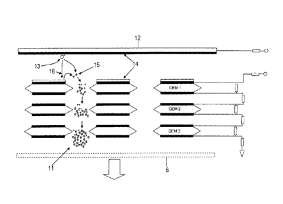
A known triple Gas Electron Multiplier detector which is
designed to detect high energy radiation will now be described with
reference to Fig. 1 for illustrative purposes only. The radiation
detector comprises three thin insulating polymer sheets 1
(GEM1,GEM2,GEM3) each typically 50 lam thick. The polymer sheets
are coated top and bottom with a thin layer 2 of copper. Small
holes 3 are etched through the polymer sheets 1 and the holes 3 are
typically 75 um diameter on a 140 pm pitch.
Voltages are applied to the copper layers 2 using a resistor
network 4 which is designed to produce an extremely high field
within the holes 3 and a lower drift field in the regions in
between the three sheets or foils (GEM1,GEM2,GEM3) and in an .
induction region between the third (final) sheet or foil (GEM3) and
a readout electrode 5.
The high field within the holes 3 penetrates a short distance
into the open space or drift region in front of the first stage
(GEM1) of the radiation detector. The high field which leaks into
the space in front of the radiation detector will act to accelerate
any negatively charged particles towards the entrance of the first
stage (GEM1) of the radiation detector. However, at the same time
the high field which leaks into the drift region in front of the
first stage (GEM1) of the detector will have the effect of
accelerating any positively charged particles away from the
entrance to the detector.
Figs. 2A and 2B show the principle of operation of the known
Gas Electron Multiplier radiation detector which is used to detect
high energy particles (e.g. particles in the MeV energy range) and
photons (e.g. x-rays and gamma rays etc). Fig. 2A shows an
incident high energy particle 6 passing through the space in front
of the entrance to the first stage (GEM1) of the radiation
detector. The high energy particle 6 ionises the ambient gas atoms
or molecules and produces both electrons 7 and positive ions 8.
The electric field leaking into the open space in front of the
entrance to the first stage (GEM1) of the radiation detector will
cause the positive ions 8 to move away from the entrance to the
detector. At the same time, the electric field will cause the
electrons 7 to move towards the holes in the first foil (GEM1).
CA 02707145 2010-05-28
WO 2009/068887
PCT/GB2008/003969
- 2 7 -
The electrons 7 enter the holes 3 in the first foil (GEM1)
and are then accelerated by the high electric field within the
holes 3 in the first foil layer (GEM1) thereby initiating a short
lived Townsend discharge. This produces more electrons as well as
positive ions within the holes in the first foil layer (GEM1).
Photons may also be produced dependent upon the ambient gas.
The positive ions which are produced within the holes in the
first foil layer (GEM1) will be attracted to the entrance electrode
forming the first foil (GEM1) whilst the electrons will proceed to
enter holes 9 in the second foil (GEM2). The electrons which enter
the holes 9 in the second foil (GEM2) will initiate a further
Townsend discharge which produces more electrons and positive ions
within the holes 9 in the second foil layer (GEM2). The process
repeats itself as electrons created within the holes 9 in the
second foil (GEM2) will then subsequently proceed to enter holes in
the third foil (GEM3) where again a Townsend discharge will be
initiated producing yet further electrons and positive ions. The
electrons 10 in the holes in the third foil (GEM3) are then
accelerated through an induction region and are collected by a
readout electrode 5 which results in a current pulse which may be
as short as 10 ns in duration. The induction region is the region
between the third foil layer (GEM3) and the readout electrode 5.
According to this arrangement the electron gain is typically of the
order 104 - 106.
Fig. 2B illustrates the conventional arrangement in the case
of ionising radiation. An incident photon 11 passing through the
drift region of the space in front of the entrance to the first
stage (GEM1) of the detector may ionise the ambient gas atoms or
molecules thereby producing electrons 7 and positive ions 8. The
process is then the same as described above with reference to the
arrangement shown in Fig. 2A. Alternately, the photon may be
incident onto a photocathode material such as a surface layer of
CsI deposited on the open or upper surface of the entrance
electrode to the first stage (GEM1) of the detector.
Photoelectrons emitted from the photocathode are attracted to the
holes 3 in the first foil (GEM1) and the avalanche process is then
the same as described above.
Fig. 3 shows a Gas Electron Multiplier ion detector according
to an embodiment of the present invention. According to a
preferred embodiment a gas avalanche electron multiplier ion
detector is provided which is arranged and adapted to detect low
energy positive ions. A counter electrode or cathode 12 is
preferably positioned in close proximity to and facing the entrance
CA 02707145 2010-05-28
W02009/068887
PCT/GB2008/003969
- 28 -
to the first stage (GEM1) of the ion detector. Analyte ions are
preferably arranged to pass between the counter electrode or
cathode 12 and the entrance to the first stage (GEM1) of the ion
detector by passing through a drift region located between the
counter electrode or cathode 12 and the upper surface of the first
stage (GEM1) of the ion detector.
According to an embodiment ions may be arranged to enter the
drift region from the side between the two surfaces i.e. between
the counter electrode or cathode 12 and the upper surface of the
first foil layer (GEM1). Alternatively, the counter electrode 12
may be made from a grid or mesh and may contain holes through which
analyte ions may pass in use. Fig. 3 shows an incident low energy
positive analyte ion 13 being attracted to the counter electrode or
cathode 12 by the application of a negative potential to the
counter electrode or cathode which may be several kV. As the
analyte ion 13 moves towards the counter electrode or cathode 12 it
may preferably collide with gas molecules in the detector or drift
region. As a result, the analyte ion 13 may be unable to attain
the impact velocity that it would otherwise have in the absence of
the gas.
The surface of the counter electrode or cathode 12 may
according to one embodiment comprise a surface coating 14, which is
preferably designed to enhance the yield of secondary negative ions
and/or secondary electrons due to low energy ion bombardment. The
impact of the incident ion 13 upon the surface of the counter
electrode or cathode 12 will preferably cause secondary negative
ions and electrons 15 to be emitted from the surface coating or
layer 14.
The number of secondary electrons emitted from a surface
undergoing ion bombardment may be described by a Poisson
distribution.
From a knowledge of the average secondary electron yield y
the probability P(n) of emitting n secondary electrons is:
(1)
n!
Hence, the probability P(0) of generating zero secondary
electrons is:
P(0) = ( 2)
CA 02707145 2010-05-28
W02009/068887
PCT/GB2008/003969
- 29 -
Hence, the probability of emitting one or more electrons may
be calculated as follows:
P(?_1)=1-P(0)=1- (3)
The actual yield will be dependent upon many factors
including the work function of the bombarded material, the mass of
the incident molecular ion, the ion elemental composition, the ion
impact angle and the ion impact velocity.
Secondary electron emission resulting from high energy (or
velocity) molecular ion bombardment of materials has been studied
and it is known that secondary electron yield decreases as the
velocity of the incident molecular ions decreases. It has
therefore previously been believed that an ion detection velocity
threshold exists around 10 to 18 mm/us below which point no
secondary electrons will be emitted. However, recent measurements
show that this is not actually the case and that some secondary
electron emission occurs for incident ion velocities as slow as 4
mm/ps. For example, Brunelle (Rapid Commun. Mass Spectrom. 1997,
353) has shown that the detection probability for a 66 kDa ion at
an impact velocity of 6 mm/us is approximately 0.2.
Brunelle and Westmacott (Nucl. Instrum. Methods B 1996, 108:
282.) have published data in the sub 20 mm/us velocity range.
Westmacott gives data from insulin (5733.5 Da), trypsin (- 23540
.Da), human tranferrin (- 79500 Da) and S-galactosidase (- 113600
Da) bombardment of stainless steel (SS) and CsI surfaces. Brunelle
shows data from Luteinizing Hormone Releasing hormone ("LHRH")
having a mass of 1182.3 Da, bovine insulin (5733.5 Da), bovine
trypsin (23296 Da) together with bovine serum albumin (66430 Da)
bombardment of CsI.
Westmacott has shown that when the so called reduced
secondary yield (7 divided by the projectile mass), is plotted
against projectile energy per unit mass (at least between approx. 5
kDa and 120 kDa) then all of the data points lie on the same curve
for a given target material. The data published by Brunelle shows
data from LHRH at 1182.3 Da which also allows the secondary yield
as a function of the projectile velocity to be determined. This
data is shown in Fig. 4 along with the data published by Westmacott
scaled to give the secondary electron yield expected by LHRH
(1182.3 Da) as a function of projectile velocity (mm/is). It is
noted that there is good agreement between the Westmacott and
Brunelle data for CsI targets. For example, a LHRH ion incident
CA 02707145 2010-05-28
W02009/068887
PCT/GB2008/003969
- 30 -
onto a surface with a velocity of 7 to 8 mm/ils would have a 7 of
0.01.
As has been previously stated Faraday cup detection systems
as used, for example, in ion mobility spectrometers require a
minimum of 103 ions and more typically 104 or more ions before a
signal may be detected. According to the preferred embodiment, for
a secondary electron yield of 0.01 then,approximately only 100 ions
are required for a signal to be detected. This is approximately
one to two orders of magnitude less than that of a conventional
Faraday cup detector and hence the preferred ion detector
represents a significant improvement in the art.
With reference back to Fig. 3, emitted secondary electrons 15
are accelerated into the holes in'the upper electrode (GEM1) which
has the effect of initiating an avalanche of electrons in a manner
as described above. Some secondary electrons 16 may, however,
strike the surface of the entrance electrode of the first stage
(GEM1) of the detector thereby causing yet further electrons to be
emitted. These further electrons are also preferably accelerated
into the holes in the first electrode (GEM1) thereby initiating an
avalanche. The exposed surface of the electrode may be coated with
a material to enhance the secondary electron yield.
In addition, positive analyte ions incident upon the surface
of the counter electrode or cathode 12 may also emit secondary
negatively charged ions 17. Under certain circumstances this may
be a more efficient detection mechanism and this embodiment now be
described in more detail with reference to Fig. 5. As shown in
Fig. 5, a low energy positive analyte ion 13 will be attracted to
the counter electrode or cathode 12 by the application of a
negative potential to the counter electrode or cathode 12. The
impact of the incident positive ion 13 upon the counter electrode
or cathode 12 may cause secondary negative ions 17 to be emitted.
The surface of the counter electrode or cathode 12 may
comprie a coating 14 to enhance the yield of secondary negative
ions due to low energy positive ion bombardment. The impact of the
incident positive ion 13 preferably causes secondary negative ions
17 to be emitted. The secondary negative ions 17 preferably drift
towards the entrance electrode of the first foil (GEM1). Upon
entering a hole in the entrance electrode of the first foil (GEM1)
the secondary negative ions 17 are preferably accelerated and this
preferably results in high energy collisions with gas molecules.
These collisions preferably yield electrons and positive ions with
the electrons 19 initiating an avalanche sequence as described
previously. It is believed that negatively charged ions may be
CA 02707145 2010-05-28
WO 2009/068887 PCT/GB2008/003969
- 31 -
stripped of their extra electron by collisional ionisation due to
the extremely high field in this region producing a neutral
molecule 18 and a free electron 19. The free electrons 19
preferably initiate an avalanche sequence as described previously.
Westmacott has presented data for the secondary negative ion
yield from CsI and stainless steel from relatively high mass
incident positive ions such as insulin, trypsin, human tranferrin
(singly and doubly charged) and g-galactosidase. It has been
reported that the efficiency for secondary negative ion emission
was between 0.4 and 0.8 irrespective of the mass and velocity of
the incident ion. In these studies the incident positive ions had
velocities in the range from 3 to 28 mm/ps. This region of
operation is indicated by the shaded area 20 in Fig. 4.
This mode of operation provides one to two orders of
magnitude higher yield than that for secondary electron emission.
According to the preferred embodiment, for a secondary negative ion
yield of approximately 0.4 to 0.8 then only approximately 1 to 3
ions may be required for a signal to be detected. This is
approximately two and a half to four orders of magnitude less than
that for a Faraday cup detector. In practice, both secondary
electron and secondary negative ion emission mechanisms are likely
to be operating simultaneously.
Examples of coatings that may be used to enhance the
secondary electron yield and/or to enhance the secondary negative
ion yield from the various surfaces as described above include, but
are not limited to, CsI, CsTe, aCH:N, Cu, Al, MgO, MgF2 and W.
Fig. 6 shows an embodiment of a gas avalanche electron
multiplier detector according to an embodiment of the present
invention which is arranged and adapted to detect low energy
negative ions. A negative potential may preferably be applied to
the counter electrode or cathode 12. This may be the same
potential as that applied previously for low energy positive ion
detection. The incident negative ion 21 is preferably repelled by
the counter electrode or cathode 12 and is accelerated directly
towards the entrance of the first stage (GEM1) of the detector.
Upon entering a hole in the entrance electrode of the first stage
(GEM1) of the detector, the secondary negative ions 21 are
preferably accelerated and this preferably results in high energy
collisions with gas molecules. These collisions preferably yield
electrons and positive ions. It is believed that negatively
charged ions can be stripped of their extra electron by collisional
ionisation due to the extremely high field in this region producing
a neutral molecule 22 and a free electron 23. The electrons 23
CA 02707145 2010-05-28
W02009/068887
PCT/GB2008/003969
- 32 -
then preferably initiate an avalanche sequence as described
previously.
There is also the possibility that the incident negative ion
21 may impact upon the electrode entrance surface of the first foil
(GEM1). In this case a secondary electron or negative ion may
result and this would be directed into one of the holes in the
first foil electrode (GEM1) producing an avalanche of electrons.
It is to be noted that in this configuration the detector
will respond to both positive and negative ions without changing
any voltages.
According to a preferred embodiment three foil electrodes may
be provided (GEM1,GEM2,GEM3) which are each 50 um thick. The foil
electrodes are preferably spaced 1 mm apart and the distance
between the first foil electrode (GEM1) and the counter electrode
or cathode 12 is preferably arranged to be 3 mm. For illustratilre
purposes only, the front or upper face of the first foil electrode
(GEM1) may be arranged to be at ground potential and a potential
difference or voltage difference of 100 V may be arranged to be
maintained across each of the foil electrodes (GEM1,GEM2,GEM3)
thereby producing an electric field of 200 kV/cm within the holes.
A potential difference or voltage difference of 30 V may be
maintained between adjacent foil electrodes (GEM1,GEM2,GEM3) and
also between the last foil electrode (GEM3) and the readout anode
5. As a result, an electric field of 3 kV/cm is preferably
maintained within these regions. The potential difference or
voltage difference between the first foil electrode (GEM1) and the
counter electrode or cathode 12 may be arranged to be -1000 V so
that the electric field in the initial drift region may be 3 kV/cm.
According to an embodiment of the present invention the
communication between the gas avalanche electron multiplier
elements may be via photo-electron emission. According to an
embodiment, a first charge blocking mesh electrode may be provided
between the first foil electrode (GEM1) and the second foil
electrode (GEM2). Anode and/or cathode strips are preferably
provided on the lower surface of the first foil electrode (GEM1).
Avalanche electrons formed within the holes in the first foil
electrode (GEM1) are preferably directed or deflected onto the
anode strips provided on the lower surface of the first foil
electrode (GEM1). As a result, a second avalanche preferably
occurs at the anode strips. Avalanche generated photons preferably
pass through the first charge blocking mesh grid and impinge upon a
photocathode surface which is preferably provided on the upper
surface of the second foil electrode (GEM2). The photocathode
CA 02707145 2010-05-28
W02009/068887
PCT/GB2008/003969
- 33 -
surface preferably comprises CsI. As a'result, photoelectrons are
preferably induced or released from the photocathode deposited upon
the upper surface of the second foil electrode (GEM2). The
photoelectrons are preferably accelerated into the holes in the
second foil electrode (GEM2) and preferably create further
avalanche electrons.
The first charge blocking mesh electrode may be polarised or
grounded such that the electric fields either side of the first
mesh electrode are reversed. Any positive avalanche ions created
within the holes in the first foil electrode (GEM1) will preferably
be directed towards the first charge blocking mesh electrode.
Similarly, any positive avalanche ions created within the holes in
the second foil electrode (GEM2) will also be directed back towards
the first charge blocking mesh electrode.
According to this embodiment ion backf low is effectively
reduced or eliminated. Furthermore, by employing an appropriately
biased intermediate grid or charge blocking electrode the transport
both of electrons and back-drifting ions between the first and
second foil electrodes (GEM1,GEM2) may effectively be blocked or
prevented.
Other embodiments are contemplated wherein additionally or
alternatively, a second charge blocking mesh or intermediate grid
may be provided between the second foil electrode (GEM2) and the
third foil electrode (GEM3). According to this embodiment, anode
and/or cathode strips are preferably provided on the lower surface
of the second foil electrode (GEM2). Avalanche electrons formed
within the holes in the second foil electrode (GEM2) are preferably
directed or deflected onto the anode strips provided on the lower
surface of the second foil electrode (GEM2). As a result, a second
avalanche preferably occurs at the anode strips. Avalanche
generated photons preferably pass through the second charge
blocking mesh grid and preferably impinge upon a photocathode
surface which is preferably provided on the upper surface of the
third foil electrode (GEM3). The photocathode surface preferably
comprises CsI. As a result, photoelectrons are preferably induced
or released from the photocathode deposited upon the upper surface
of the third foil electrode (GEM3). The photoelectrons are
preferably accelerated into the holes in the third foil electrode
(GEM3) and preferably create further avalanche electrons.
The second charge blocking mesh electrode may be polarised or
grounded such that the electric fields either side of the second
mesh electrode are reversed. Any positive avalanche ions created
within the holes in the second foil electrode (GEM2) will
CA 02707145 2010-05-28
W02009/068887
PCT/GB2008/003969
- 34 -
preferably be directed towards the second charge blocking mesh
electrode. Similarly, any positive avalanche ions created within
the holes in the third foil electrode (GEM3) will also be directed
back towards the second charge blocking mesh electrode.
According to an embodiment which is given for illustrative
purposes only, three foil electrodes may be provided
(GEM1,GEM2,GEM3) which are each 50 um thick and spaced 2 mm apart
from each other. The distance between the first foil electrode
(GEM1) and the counter electrode or cathode 12 is preferably
arranged to be 3 mm. Two charge blocking mesh electrodes may be
provided which are preferably located at the midpoint between the
three foil electrodes (GEM1,GEM2,GEM3). The front or upper face of
the foil electrodes (GEM1,GEM2,GEM3) may be connected to ground
potential. The voltage difference or potential difference across
the holes in the foil electrodes between the upper electrode on a
foil electrode and the lower electrode cathode strip may be
arranged to be 100 V. The voltage between the anode strips and the
cathode strips on the lower electrode of the foil electrodes
(GEM1,GEM2,GEM3) may be arranged to be 20 V (i.e. 120 V w.r.t.
ground). The charge blocking mesh electrodes are preferably
connected to ground potential and the potential between the last
foil electrode (GEM3) and the readout anode 5 may be arranged to be
30V (i.e. 150 V w.r.t. ground). The voltage difference between the
first foil electrode and the counter electrode or cathode 12 may be
arranged to be -1000 V.
A further embodiment is contemplated wherein the readout
electrode 5 may be replaced by a photo-multiplier tube or by a CCD
camera. The photo-multiplier tube or CCD preferably add further
gain to the overall ion detector and thereby enables the previous
Gas Electron Multiplier stages to be operated with lower gain. As
a result, the Gas Electron Multiplier stages can be maintained at
lower voltages. The use of a CCD camera detector also enables the
ion detector to be used for recording images in applications where
spatial information is of value.
According to another embodiment an additional Gas Electron
Multiplier stage (GEMO) may be provided prior to the first Gas
Electron Multiplier stage (GEM1) of the ion detector. A positive
potential may be applied to the counter electrode or cathode 12 in
order to repel positive analyte ions. The potential between the
entrance and exit electrodes of the additional Gas Electron
Multiplier stage (GEMO) may be arranged such that positive analyte
ions are attracted to and accelerated within the holes of the
entrance electrode of the additional Gas Electron Multiplier stage
CA 02707145 2010-05-28
WO 2009/068887
PCT/GB2008/003969
- 35 -
(GEMO) . Upon entering a hole in the entrance electrode of the
additional stage (GEMO) the positive analyte ions may be
accelerated and collide with the ambient gas molecules. The
collisions may be arranged such that the analyte ions become
excited (e.g. into a metastable state) promoting electrons to
higher energy states. As a result, photons may be emitted upon
relaxation of the promoted electrons to ground states. The photons
which are emitted as a result of the metastable ions relaxing to a
ground state may then be arranged to be incident upon a
photocathode material which is preferably deposited on the entrance
electrode of the first Gas Electron Multiplier stage (GEM1) thereby
releasing photoelectrons. The photoelectrons are then preferably
arranged to be incident into the entrance holes of the first Gas
Electron Multiplier stage (GEM1) initiating an avalanche sequence
as described above.
According to an embodiment as shown in Fig. 7 an apparatus
may be provided comprising a source of ions and a means or device
of sampling the ions 24. An ion mobility separator 25 may be
arranged downstream of the ion source and the means or device 24
for sampling the ions. At least some of the ions are preferably
separated according to their ion mobility or rate of change of ion
mobility with electric field strength in the ion mobility separator
25. An ion detector 26 according to the preferred embodiment is
preferably provided downstream of the ion mobility spectrometer 25.
A particularly advantageous feature of this embodiment is that both
the ion mobility spectrometer 25 and the ion detector 26 according
to the preferred embodiment may be maintained at a relatively high
pressure thereby avoiding the need for expensive and complicated
high vacuum pumping systems. The overall apparatus may comprise a
hand held and/or otherwise portable device. Alternatively, the ion
mobility spectrometer including an ion detector 26 according to the
preferred embodiment may comprise a static or essentially fixed
device.
At the upstream end of the apparatus, the ion source 24 may
comprise a pulsed ion source such as a Laser Desorption Ionisation
(LDI) ion source, a Matrix Assisted Laser Desorption Ionisation
("MALDI") ion source or a Desorption Ionisation on Silicon ("DIOS")
ion source.
Alternatively, a continuous ion source may be used in which
case an ion gate for creating a pulse of ions may be provided. The
ion gate is preferably arranged to pulse ions into the ion mobility
spectrometer. According to another embodiment an ion trap for
storing ions and periodically releasing ions may be provided. The
CA 02707145 2010-05-28
WO 2009/068887 PCT/GB2008/003969
- 36 -
ion trap may be arranged to periodically release ions in packets or
pulses so that packets or pulses of ions subsequently enter into
the ion mobility spectrometer.
Continuous ion sources which may be used include an Electron
Impact ("El") ion source, a Chemical Ionisation ("CI") ion source,
an Electrospray Ionisation (ESI) ion source, an Atmospheric
Pressure Chemical Ionisation ("APCI") ion source, an Atmospheric
Pressure Photon Ionisation ("APPI") ion source, a Fast Atom
Bombardment ("FAB") ion source, a Liquid Secondary Ion Mass
Spectrometry ("LSIMS") ion source, a Field Ionisation ("Fl") ion
source or a Field Desorption ("FD") ion source. Other continuous
or pseudo-continuous ion sources may also be used.
The ion mobility separator 25 preferably comprises a device
that causes ions to become temporally separated based upon or
according to their ion mobility. The ion mobility spectrometer may
have a number of different forms.
According to an embodiment the ion mobility spectrometer or
separator may be provided in chamber that is preferably maintained,
in use, at a pressure at or above atmospheric pressure. According
to another embodiment the ion mobility spectrometer or separator
may be provided in a vacuum chamber that is preferably maintained,
in use, at a pressure within the range 0.1-10 mbar. According to
other embodiments, the vacuum chamber may be maintained at a
pressure greater than 10 mbar up to a pressure at or near
= atmospheric pressure. According to less preferred embodiments, the
vacuum chamber may be maintained at a pressure below 0.1 mbar.
In one embodiment, the ion mobility separator 25 may comprise
an ion mobility separator comprising a drift tube having a number
of guard rings distributed within the drift tube. The guard rings
may be interconnected by equivalent valued resistors and connected
to a DC voltage source. A linear DC voltage gradient may be
generated along the length of the drift tube. The guard rings are
not connected to an AC or RF voltage source.
According to another embodiment the ion mobility spectrometer
or separator 25 may comprise a number of ring, annular or plate
electrodes, or more generally electrodes having an aperture therein
through which ions are transmitted. The ion mobility separator may
comprise a plurality of electrodes arranged in a chamber at low
pressure or under a partial vacuum. Alternate electrodes forming
the ion mobility separator are preferably coupled to opposite
phases of an AC or RF voltage supply. The AC or RF voltage supply
preferably has a frequency within the range 0.1-10.0 MHz,
preferably 0.3-3.0 MHz, further preferably 0.5-2.0 MHz.
CA 02707145 2014-03-19
- 37 -
The electrodes comprising the ion mobility spectrometer or
separator are preferably interconnected via resistors to a DC
voltage supply. The resistors interconnecting electrodes forming
the ion mobility spectrometer or separator may be substantially
equal in value in which case an axial DC voltage gradient is
preferably obtained. The DC voltage gradient may be linear or
stepped. The gradient may be applied so to propel ions towards the
detector or towards the source. The applied AC or RE voltage is
preferably superimposed upon the DC voltage and serves to confine
ions radially within the ion mobility spectrometer or separator.
According to another preferred embodiment of the present
invention the ion mobility spectrometer or separator 25 may
comprise a travelling wave ion guide comprising a plurality of
electrodes. Adjacent electrodes are preferably connected to the
opposite phases of an AC or RE supply. Transient DC voltages are
preferably applied to one or more electrodes to form one or more
potential hills or barriers. Transient DC voltages are preferably
progressively applied to a succession of electrodes such that the
one or more potential hills or barriers move along the axis of the
ion guide in the direction in which the ions are to be propelled or
driven which may be towards the ion source or towards the ion
detector 26.
The presence of gas within the ion mobility spectrometer
preferably imposes a viscous drag on the movement of ions through
the ion mobility spectrometer 25. The amplitude and average
velocity of the one or more potential hills or barriers which is
preferably applied in a transient manner to the electrodes forming
the ion mobility spectrometer 25 is preferably set such that ions
will, from time to time, slip over a potential hill or barrier. The
lower the mobility of the ion the more likely the ion will slip
over a potential hill or barrier. This in turn allows ions of
different mobility to be transported at different velocities and
thereby separated as the one or more transient DC voltages or
potentials is applied to the electrodes forming the ion mobility
spectrometer.
According to another embodiment the ion mobility spectrometer
or separator 25 may comprise a device as described in
W02006/085110. The device or ion mobility spectrometer may
preferably comprise an upper planar electrode, a lower planar
electrode and a plurality of intermediate electrodes. An ion
guiding region is preferably formed within the ion guide. An
asymmetric voltage waveform is preferably applied to
CA 02707145 2014-03-19
- 38 -
the upper electrode and a DC compensating voltage is preferably
applied to the lower electrode.
According to another embodiment the ion mobility spectrometer
or separator 25 may comprise a device as described in WO
2006/059123. The ion mobility spectrometer or device may preferably
comprise one or more layers of intermediate planar, plate or mesh
electrodes. A first array of electrodes is preferably provided on
an upper surface and a second array of electrodes is preferably
arranged on a lower surface. An ion guiding region is preferably
formed within the ion guide. One or more transient DC voltage or
potentials are preferably applied to the first and/or second array
of electrodes in order to urge, propel, force or accelerate ions
through and along the ion guide.
According to an embodiment the detector according to the
preferred embodiment may be used with a differential ion mobility
separator or with a Field Asymmetric Ion Mobility Spectrometer
("FAIMS") device.
According to another embodiment the ion mobility spectrometer
or separator 25 may be of the form described in W02004/109741. The
ion mobility spectrometer is preferably arranged to extract ions by
entraining ions in a laminar flow of a carrier gas. A barrier
region is preferably provided and an electrical field is preferably
applied across the laminar flow of the carrier gas. The magnitude
and direction of the electrical field is preferably selected so as
to prevent at least some of the ions entrained in the laminar flow
from passing through the electrical field. The electrical field is
preferably varied to allow ions having predetermined
characteristics to pass through the electrical field.
The ion detector 26 according to the preferred embodiment
preferably comprises a gas avalanche electron multiplication
device that is preferably configured to detect both low energy
positive and low energy negative ions.
According to another embodiment as shown in Fig. 8 a mass
spectrometer is preferably provided which preferably comprises a
source of ions and a means of or device for sampling the ions 24.
The mass spectrometer preferably comprises a mass analyser 27 and
an ion detector 26. The apparatus or mass spectrometer may
comprise a hand held and/or portable device. Alternatively, the
mass spectrometer may comprise a static or fixed device.
At the upstream end of the apparatus or mass spectrometer, an
ion source 24 may be provided. The ion source preferably comprise
CA 02707145 2014-03-19
- 39 -
a pulsed ion source such as a Laser Desorption Ionisation ("LOT")
ion source, a Matrix Assisted Laser Desorption Ionisation ("MALDI")
ion source or a Desorption Ionisation on Silicon ("DIOS") ion
source. Alternatively, a continuous ion source may be used. The
continuous ion source may comprise an Electron Impact ("El") ion
source, a Chemical Ionisation ("CI") ion source, an Electrospray
Ionisation ("ESI") ion source, an Atmospheric Pressure Chemical
Ionisation ("APCI") ion source, an Atmospheric Pressure Photon
Ionisation ("APPI") ion source, a Fast Atom Bombardment ("FAB") ion
source, a Liquid Secondary Ion Mass Spectrometry ("LSIMS") ion
source, a Field Ionisation ("Fl") ion source and a Field Desorption
("FD") ion source. Other continuous or pseudo-continuous ion
sources may also be used.
In one embodiment the mass spectrometer may be operated at or
near atmospheric pressure and may be of the form as disclosed in
GB-2369722. According to this embodiment a mass spectrometer may
be provided comprising an ion source and a centrifuge mass
separator. A mass analyser is preferably arranged downstream of
the ion source and centrifuge mass separator. The centrifuge mass
separator preferably comprises a chamber having a sample inlet and
an inlet for a drying gas. At least one of the inlets is
preferably arranged so as to tangentially inject a sample or
drying gas into the chamber. In use a centrifugal force may be
used to separate particles within the chamber.
In another embodiment the mass spectrometer may operated at a
pressure in the range from 0.1 mbar to 10 mbar, and may use the
mass selection principles disclosed in WO 2008/071967. According
to this embodiment, a mass spectrometer may be provided comprising
a device for separating ions temporally. In a first mode of
operation the device is arranged and adapted to separate ions
temporally according to their ion mobility. In a second mode of
operation the device is arranged and adapted to separate ions
according to their mass to charge ratio.
According to another embodiment the mass spectrometer may
comprise a device as disclosed in W02005/067000. According to this
embodiment ions are supplied in a body of a gas. A ponderomotive
ion trapping potential is preferably generated generally along an
axis. Further potentials are preferably generated to provide an
effective potential which prevents ions from being extracted from
an extraction region. Ions are preferably arranged to be trapped
in
CA 02707145 2014-03-19
- 40 -
the effective potential. The device preferably further comprises a
device to selectively extract ions having a predetermined mass to
charge ratio or ion mobility from the extraction region. The
characteristics of the effective potential which prevents ions from
being extracted from the extraction region is preferably caused at
least in part by the generation of the ponderomotive ion trapping
potential.
According to another embodiment the mass spectrometer may
comprise a device as disclosed in W02007/010272. The mass
spectrometer preferably comprises a mass or mass to charge ratio
selective ion trap comprising a plurality of electrodes. A first
mass filter or mass analyser is preferably arranged downstream of
the mass or mass to charge ratio selective ion trap. A control
device is preferably provided which is preferably arranged and
adapted to cause ions to be selectively ejected or released from
the ion trap according to their mass or mass to charge ratio. The
control device is also preferably arranged to scan the first mass
filter or mass analyser in a substantially synchronised manner with
the selective ejection or release of ions from the ion trap.
According to other embodiments the mass spectrometer may be
operated at a pressure less than 0.1 mbar or greater than 10 mbar.
Other embodiments are also contemplated wherein multiple
stages of separation may be employed in tandem. For example, a
configuration is contemplated comprising a source of ions and a
means of sampling these ions. An ion mobility spectrometer or
separator followed by d mass spectrometer may preferably be
provided downstream of the ion source. An ion detector according
to the preferred embodiment is preferably provided as part of the
mass spectrometer.
The scope of the claims should not be limited by the
preferred embodiments set forth in the examples, but should be
given the broadest interpretation consistent with the description
as a whole.