Note: Descriptions are shown in the official language in which they were submitted.
CA 02707225 2010-06-10
SUPERCONDUCTIVE ELEMENT AND RELATIVE
PREPARATION PROCESS
The present invention relates to a superconductive
element and the relative preparation process.
The present invention is included in the technical
field of superconductive materials.
In the different industrial application in which
superconductive materials are used, it must be
guaranteed that these materials have suitable
characteristics of thermal and mechanical stability, in
addition to specific electrotechnical functionalities.
In the state of the art, superconductive materials
are normally prepared in the form of wires, thick or
thin strips or in the form of massive bodies. The wires
and strips, normally having a thickness of less than 1
millimetre, are assembled together with supports made
of non-superconductive material of the metallic or
electrical insulating type. The function of the
supports is to give the superconductive material
suitable characteristics of mechanical strength in
addition to suitable electrical and thermal
characteristics, when necessary. The assembly of the
superconductive wire or strip with a support, however,
substantially reduces the section of wire or strip
available for the passage of superconductive currents.
-1-
CA 02707225 2010-06-10
In extreme cases, the ratio between the above section
and the overall section of the supported wire or strip
can drop to values lower than 20-30% of the original
value of the superconductive wire or strip, drastically
reducing the density of the superconductive current
conveyed.
Fault current limiters consisting of
superconductive inserts enclosed in non-superconductive
supports are also described in literature. These fault
current limiters, however, have an application field
limited to low currents. They are in fact based on
superconductive inserts produced with superconductive
materials, such as superconductive oxides in
polycrystalline form, which, due to the barriers
between the crystalline grains, do not have a critical
current density which is such as to allow them to be
also used for other electrotechnical applications, such
as those having high magnetic fields. In particular,
their critical current density is not capable of
producing economical magnetic field flux density
comparable or better than those which can be produced
with normal electromagnets or with classical permanent
magnets, typically limited to values below 1 tesla.
Unlike wires or strips, superconductive currents
can pass through the whole section of superconductive
-2-
CA 02707225 2010-06-10
materials in the form of massive bodies. They are
generally prepared in the form of plates, cylinders,
rings or pipes having a thickness of various
millimetres. When the superconductive material is
malleable, such as, for example, Pb and Nb
(superconductive materials at temperatures lower than 9
K), they can also be prepared in the form of thin
sheets or laminas.
For applications at temperatures higher than 10 K,
superconductive massive bodies can consist of:
- ceramic oxides, such as for example cuprates
based on yttrium and barium (superconductive up
to the critical temperature, Tc, of about 90 K)
or based on strontium, such as for example
Sr2CuO34 4 (Tc = 95K) or based on bismuth,
strontium and calcium (Tc = 110 K),
- iron-based materials, such as for example,
FeTeo.SSeo5 S (Tc = 13 K) or Bao.6Ko.4Fe2As2 (Tc = 38
K) or FeAsNdOo.85 (Tc = 51 K) ,
- magnesium diboride (Tc = 39 K),
- intermetallic compounds, such as for example
Nb3Sn (Tc = 18. 7 K) , Nb3Al (Tc = 21. 3 K) or Nb3Ge
(Tc = 23.6 K).
The best performances, in terms of critical current
density, are generally obtained with massive materials
-3-
CA 02707225 2010-06-10
in a highly densified form, in particular when they are
in a state of high crystalline perfection (mono-
crystalline state).
The preparation of superconductive massive
materials in a highly densified form and in mono-
crystalline state, however, is not easy to do. The
growth and orientation process of the crystalline
grains, in fact, is a rather lengthy and complex
process, which requires in particular a careful
temperature control during the crystallization process
and which leads to superconductive end-products having
a maximum dimension limited to a few centimetres.
Among the above superconductive materials produced
in massive form and having a critical temperature
higher than 10 K, magnesium diboride (MgB2) can be
distinguished for being able to be usefully adopted
also in polycrystalline form. This is possible as the
passage of the superconductive currents in this
material is not greatly influenced by the passage of
the boundaries between the crystalline grains and
orientation of the grains themselves.
A further distinctive characteristic of magnesium
diboride is that it can be prepared in a highly
densified form.
Analogously to other superconductive materials
-4-
CA 02707225 2010-06-10
having a critical temperature higher than 10 K,
magnesium diboride, however, is a fragile material and
therefore also requires adequate mechanical
reinforcement to allow it to be effectively used in
most of its applications. An adequate mechanical
strength, in particular, is indispensable in
applications characterized by the presence of
particularly intense electromagnetic forces, such as,
for example, in magnets for high magnetic fields where
the electric currents in question are in the order of
thousands of amperes and the magnetic field flux
densities are generally higher than 1 tesla.
In most applications, however, the use of massive
superconductive end-products having a considerable
thickness (in the order of a centimetre or higher),
regardless of the superconductive material, is not
convenient. This is due, on the one side, to the fact
that the superconductive currents tend to be
distributed on only a part of the superconductive end-
product (prevalently on the surface) and, on the other,
to the fact that great thicknesses prevent a rapid
cooling of the superconductive material when, during
its functioning, there are transitions from the
superconductivity state to that of normal conduction,
accompanied by the instantaneous release of high
-5-
CA 02707225 2010-06-10
quantities of heat energy.
A further technical problem of superconductive
devices with inserts on rigid supports known in the
state of the art lies in the fact that with the known
techniques, it is not always possible to produce these
devices in the desired form and dimensions.
In order to obtain sintered bodies of particularly
dense ceramic materials and when the type of material,
for thermodynamic reasons, prevents its spontaneous
sintering at atmospheric pressure, hot pressing
densification techniques can be used. These techniques
comprise applying a pressure to the pre-compacted
ceramic powders, at typical sintering temperatures
(approximately about 3/4 of the absolute melting
temperature of the material) to favour the sintering
process. The temperatures generally range from 700 C to
1600 C and the pressures can reach various hundreds of
atmospheres. Depending on the procedure with which the
pressure is applied, there can be: a) uniaxial
compression, b) isostatic compression. For uniaxial
compression, presses having the powder container and
compression piston generally made of graphite are used,
which can be heated for example by induction or with
specific resistors made of silicon carbide. The main
disadvantage of this technique is due to the mechanical
-6-
CA 02707225 2010-06-10
resistance of the container, which considerably limits
the dimensions of the pieces to be pressed.
Uniaxial compression is therefore suitable for
producing end-products which have extremely different
dimensions in the two spatial directions (for example,
plates or laminas), so that there are no large
deformations in a direction perpendicular to that of
the pressure application.
Isostatic compression uses a hot gas as fluid for
transferring the pressure applied to the powders to be
sintered. Isostatic compression is effected in a
machine comprising a large pressure-sealed chamber in
which the piece to be densified is inserted, covered
either with a 'metal sheath or a layer of vitreous
material which becomes plastic at high treatment
temperatures, so as to assist the pressure transfer
from the gas to the piece. Even with this technique,
the dimensions of the superconductive end-products that
can be produced are limited to a few tens of cm.
Considering the limits of the techniques described
above, it is evident that these techniques are of
little use in the preparation of devices with
superconductive inserts inlayed on rigid supports, for
example made of metal or ceramic material, which offer
a high mechanical resistance. In particular, with the
-7-
CA 02707225 2010-06-10
uniaxial technique it is not possible to produce device
having supports with a non-planar geometry.
In the case of materials which require a hot
pressing, the form of the inlays prevents an adequate
and simple application of the pressure to the powders,
as the structure of the substrate hinders, as in the
case of uniaxial pressure on a non-planar substrate, a
direct transfer of the deformation to the powder. Also
in the isostatic case, the substrate is a great
hindrance to the pressure transfer on the powders, as
only deformations of the material which covers the
powder on the exposed surface of the inlay and in the
direction perpendicular to this, are effective.
In the state of the art, in order to prepare
superconductive devices comprising superconductive
inserts on rigid supports, resort is also made to the
melt densification technique. US 5,426,408, for
example, describes flat supports having one side made
of a conductive material and the opposite side made of
an insulating material. The inserts are made of
superconductive material based on bismuth or yttrium
copper oxides. The inserts are prepared by distribution
of the superconductive material on the surface of the
support (screen printing) and subsequent thermal
treatment at the melting point of the superconductive
-8-
CA 02707225 2010-06-10
material (melt densification). US 5,426,408 also
describes superconductive magnetic modules consisting
of a plurality of the above devices, connected to each
other by means of holes in the support filled with
superconductive material. These superconductive
connections put the insert of a first device in
electric contact with that of a second device. The
superconductive inserts of the devices and magnetic
modules described in US 5,426,408, however, have a very
limited thickness, varying within the range of 50-200
pm. Furthermore, in the case of superconductors based
on yttrium copper oxides, the density of the
superconductive material obtainable in the inserts and
in the superconductive connections with the technique
described above, is at the most equal to about 70% of
its theoretical density. This is known to experts in
the field, for example, from the publication of J. 0.
Willis et al. in IEEE TRANSACTIONS ON MAGNETICS, Vol.
25, No. 2, March 1989, 2502-2504.
The document EP 0503447 describes superconductive
devices consisting of superconductive inserts on non-
superconductive rigid supports. Also in this case, the
conductive inserts are obtained by means of the so-
called "melt densification" technique. As already
mentioned, however, this technique does not allow
-9-
CA 02707225 2010-06-10
inserts of superconductive material with a high density
to be obtained. The devices described in EP 0503447
consequently also have a limited capacity of
transporting high current densities.
An objective of the present invention is to
overcome the drawbacks revealed in the state of the
art.
A first object of the present invention relates to
a superconductive element comprising a rigid support
made of a non-superconductive material, said support
comprising at least one superconductive track formed by
a groove containing a superconductive material having a
real density equal to at least 85% of the value of its
theoretical density, preferably equal to at least 88%.
A second object of the present invention relates to
a process for preparing a superconductive element
comprising the following operative steps:
a) making at least one groove on the surface of a rigid
support made of non-superconductive material;
b) inserting a powdered precursor of a superconductive
material inside the groove and compacting it up to a
real density value equal to at least 50% of the
theoretical density value;
c) positioning at least one solid reactant in contact
with the precursor powder or else in a position adjacent
-10-
CA 02707225 2010-06-10
to the groove in which the powder is contained;
d) subjecting the reactant and the groove containing the
precursor to heating until the reactant is liquefied and
subsequently infiltrates inside the precursor powder
with formation of a superconductive track inside the
groove.
For a better understanding of the characteristics
of the present invention, in the description reference
will be made to the following figures:
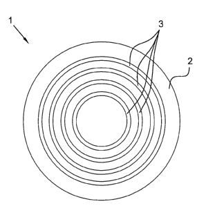
- figure 1, schematic representation of a view
from above of a superconductive element according to
the present invention;
- figure 2, schematic representation of a
vertical section of a superconductive element according
to the present invention enclosed in a reaction
container having a sealable lid;
- figure 3, schematic representation of a view
from above of a further embodiment of a superconductive
element according to the present invention;
- figure 4A, schematic representation of a
possible connection mode between two superconductive
tracks of the same superconductive element by means of
a superconductive filament;
figure 4B, schematic representation of a
superconductive device comprising two superconductive
-11-
CA 02707225 2010-06-10
elements connected to each other by means of a
superconductive filament which connects two
superconductive tracks belonging to two different
superconductive elements;
- figure 5, schematic representation of a
superconductive element having inlays of the helicoidal
type;
figure 6, graph of the critical current Ic
trend (expressed in amperes) in relation to the
magnetic flux density B (expressed in tesla), measured
at 4.2K on the superconductive element of example 1;
- figure 7A, plan view from above of a schematic
representation of a superconductive element in the form
of a strip consisting of parallel interwoven inlays;
- figure 7B, section according to the plane A-A'
of figure 7A;
- figure 7C, section according to the plane B-B'
of figure 7A.
The superconductive element, object of the present
invention, comprises a rigid support made of a non-
superconductive material on whose surface at least one
conductive track is etched of a superconductive
material having a section of a few mm2.
With reference to the embodiment illustrated in
figure 1, a superconductive element 1 object of the
-12-
CA 02707225 2010-06-10
present invention consists of a support 2, in this case
a circular disk, containing on its surface circular
superconductive tracks 3, arranged in the form of
concentric rings.
The superconductive track 3 of the superconductive
element 1 can be produced with any superconductive
material, provided it has a density higher than or
equal to 850 of the value of its theoretical density.
The density is preferably higher than 880. Preferred
superconductive materials are the following: MgB2,
FeNdAsO0.85 , FeTeo, 5Seo . 5 , Sr2CuO3.4 .
A particularly preferred embodiment of the present
invention is a superconductive element in which the
conductive tracks comprise MgB2 as superconductive
material, as tracks consisting of MgB2 can be prepared
in a highly densified form in a much simpler way than
other known superconductive materials in the state of
the art and they do not have problems relating to a
limited current density due to the presence of grain
boundaries in the usual polycrystalline form.
For the purposes of the present invention, the term
"highly densified" refers to a material having a
density higher than or equal to 850 of the value of its
theoretical density.
A conductive track consisting of a thin inlay of a
-13-
CA 02707225 2010-06-10
superconductor in a highly densified form gives the
superconductive element higher electric current
transmission properties with respect to the same
superconductive elements having tracks produced with
other types of less densified superconductive
materials. In addition, the reduced thickness of the
useful track, deriving from its higher density, favours
a more rapid cooling of the superconductive material
and a less destructive dispersion of the
superconductive streams during transition to the normal
conduction state.
A further advantage of a superconductive element
with inlays is that it can also be produced with tracks
having a helicoidal development inlayed around the
surfaces of the support. The helicoidal inlays allow
the formation of windings which simulate the braiding
of wires. This morphology of the superconductive
windings is particularly useful in magnets with a high
magnetic field to reduce phenomena of instability, when
there are current transients as occurs in charging or
with uses in alternating current.
Another advantage of a superconductive element with
inlays is that it can be produced in the form of a
strip consisting of the intersecting of groups of
parallel superconductive tracks, overlapping each
-14-
CA 02707225 2010-06-10
other. The strips with superconductive tracks can be
produced with forming processes of the grooves of the
support, such as shear cutting or laser cutting, for
example. The whole preparation process of the
superconductive element can be effected in continuous,
and comprises operations for charging the precursor
materials inside the grooves, positioning the reactants
and thermal treatment, in succession. In this way, it
is possible to produce strips in any desired length.
The support of the superconductive element, object
of the present invention, is a rigid support made of a
non-superconductive material, having any geometrical
form.
The form of the support is selected in relation to
the use for which the superconductive element is
destined. The support is preferably in the form of a
plate, disk, ring, strip or hollow cylinder having a
thickness ranging from 2 mm to 30 mm, preferably from 3
to 20 mm. Regardless of its form, it is possible to
prepare grooves on the whole surface of the support,
pass-through or not: in the case of planar supports,
for example in the form of a plate or disk, grooves can
be engraved on both of the main sides of the support,
i . e . on the sides having a larger surface; in the case
of hollow cylindrical supports, the tracks can be
-15-
CA 02707225 2010-06-10
inlayed on both the internal and external surface of
the cavity. In the following description of the present
invention, the term "surface of the support" refers to
the overall surface of the support available for the
inlaying of the grooves.
The material of the support is a non-
superconductive material, preferably a material with a
low electric conductivity, high mechanical
characteristics and melting temperature more than 400 C
degrees higher that the reaction temperature to obtain
the superconductive element . Examples of materials
suitable for the production of the support are non-
magnetic stainless steel, iron/nickel alloys, nickel
and nickel/copper alloys with a high nickel content,
i.e. higher than 506, titanium, composites of these
materials with copper, and also intermetallic compounds
having a melting point higher than 1100 C, such as for
example a zinc-tellurium compound.
In most cases of superconductive elements destined
for electromagnetic applications, the material of the
support must be non-magnetic. In these cases, it is
preferable to use supports made of AISI 316 steel or
nickel-copper alloys of the Monel type.
The material which forms the support must be
resistant to the treatment applied to obtain the
-16-
CA 02707225 2010-06-10
transformation of the precursor powder, positioned
inside the groove, in a strip of superconductive
material, i.e. in the superconductive track. The
conversion of the precursor to superconductive material
takes place by means of a treatment comprising a high-
temperature chemical reaction between the precursor and
one or more additional reactants. The precursor in
powder form is inserted in the groove and the other
reactants, preferably in the form of massive bodies,
are placed outside the groove in such a position that,
once liquefied as a result of the heating, they can
enter into contact with the precursor.
For the purposes of the present invention, the term
"precursor" indicates a solid material in powder form
which, if subjected to suitable physico-chemical
treatment, modifies its crystalline nature, becomes
densified and acquires superconductive properties
useful for the passage of the current. The precursor
can also be a first component of a superconductive
material which, by chemical reaction with a second
component, is transformed into a superconductive
material.
Figure 2 schematically represents a vertical
section of an end-product which can be used for
obtaining a superconductive element according to the
-17-
CA 02707225 2010-06-10
present invention. A reactant 6, necessary for the
above conversion, in the form of a solid body
superimposed with respect to the support 2 and the
grooves containing the precursor (tracks 3) is inserted
inside a container 4 (reaction container) having a lid
5, sealed for effecting the conversion treatment of the
precursor to superconductive material.
Undesired reactions between the support and
precursor or between the support and other reactants
necessary for the conversion of the precursor to
superconductive material can be avoided by suitably
selecting the material of the support in relation to
the reactants used, and also by applying a thin coating
film of an inert refractory material (not shown in the
figures) onto the support 2. The thickness of the film
applied is preferably equal to about 0.5 - 20 microns.
The coating film is applied after tracing the
grooves on the support, so as to coat both the surface
of the support and the internal surface of the grooves.
The material of the coating film is selected in
relation to the superconductive material with which the
conductive tracks are to be produced. Coating films
made of an electric insulating material of the oxide
type, preferably films consisting of MgO, SiO2, A12O3,
NiO, Fe2O3, TiO2, ZnO, ZrO2, Y203 or their compounds or
-18-
CA 02707225 2010-06-10
coating films of the metallic type of Fe, Ni or Ti, are
preferably used.
The films can be applied to the surface of the
support and grooves with techniques known in the state
of the art. The application of the coating film by
means of oxidation techniques or the deposition of
materials in vapour phase, such as for example the
technique called Chemical Vapour Deposition (CVD), is
particularly preferred.
The grooves on the surface of the support can be
produced with the conventional processing techniques
known in the state of the art, such as milling,
turning, cutting or electric-erosion inlaying. The
grooves can be produced in various forms and
dimensions. The grooves traced on the support generally
have a depth/width (D/W) ratio equal to or higher than
0.5, preferably higher than 1, even more preferably
higher than 2. For thicknesses of the support ranging
from 2 to 20 mm, the width of the groove is preferably
less than or equal to 3 mm and its depth varies from
1.5 to 9 mm. It is useful at times to create grooves
with a variable section, along their linear
development, to better respond to the electromagnetic
requirements of the superconductive element. It is
possible however to reduce the depth of the
-19-
CA 02707225 2010-06-10
superconductive track to D/W values lower than 0.5, in
the finishing phase, in order to satisfy specific
applicative demands.
The support of the superconductive element can have
superconductive tracks of the open or closed type. A
"closed" track is a superconductive track obtained
starting from a groove which defines a closed line on
the support, such as, for example, the grooves of the
tracks 3 of figure 1 or the combination of grooves of
the tracks 3 and 7 of figure 3.
An "open" track is a conductive track obtained
starting from a groove which defines an open line on
the support, i.e. a line having two ends terminating in
distinct points of the support, such as for example,
the lines connecting points 8 and 9 or the points 8'
and 9' of the track 3 of figure 3. In a preferred
embodiment, the open tracks are helical, i.e. with a
helicoidal development.
When a superconductive element, object of the
present invention, comprises closed tracks and an
electric current passes through said tracks, the
superconductive element acts as a permanent magnet
having a magnetization which is fairly constant with
times of interest for the applications.
When a superconductive element comprises open
-20-
CA 02707225 2010-06-10
tracks and an electric current passes through said
tracks, the superconductive element produces a variable
magnetic field in relation to the current intensity
which passes through the tracks.
The closed tracks can have any form. A closed track
can also consist of open tracks situated in different
areas of the surface of a same support (for example,
two opposite sides of a flat support), said tracks
being connected to each other by superconductive
filaments or, in the case of two opposite sides of a
support, holes in the support filled with
superconductive material. The holes filled with
superconductive material are hereafter also indicated
as superconductive pass-throughs. The superconductive
pass-throughs join any two points belonging to two
distinct grooves.
A superconductive element according to the present
invention can contemporaneously comprise one or more
open and/or closed conductive tracks.
In a preferred embodiment, the superconductive
element having closed tracks, object of the present
invention, comprises one or more circular-shaped
concentric tracks (figure 1) . In a second preferred
embodiment, the superconductive element has spiral-
shaped open tracks inlayed on opposite sides of a flat
-21-
CA 02707225 2010-06-10
support or along the opposite walls of a cylindrical
support, said tracks being connected to each other by
two superconductive pass-throughs.
A further object of the present invention relates
to a superconductive device comprising a first and a
second superconductive element, each having at least
one open track, wherein a first open track of a first
superconductive element is connected by means of one or
more superconductive filaments to a second open track
of a second superconductive element. The supports of
the superconductive elements which form the
superconductive device can possibly be electrically
connected to each other.
The open tracks of a superconductive element can be
connected to each other by means of one or more
superconductive filaments. These superconductive
filaments are made integral with the superconductive
material of the tracks, by entrapping the ends of the
filaments between the precursor powder of the
superconductive material inserted in the groove and
effecting the precursor-superconductor conversion
reaction in the presence of these filaments. In
particular, the superconductive tracks to be connected
can belong to the same superconductive element (figure
4B) or to distinct superconductive elements, i.e.
-22-
CA 02707225 2010-06-10
forming a superconductive device (figure 4A). In this
latter case, the superconductive elements can be
connected to each other in series or parallelly.
To give greater mechanical strength to the
superconductive devices of the present invention, the
superconductive elements can be connected to each
other, for example, by means of connection stands
between the supports made of a non-superconductive
material. In the same way, to mechanically reinforce
the superconductive filaments connected to the
superconductive elements, the superconductive filaments
can be inserted in specific grooves situated on the
same support as that of the superconductive element or
on additional supports. The superconductive filaments
can be kept in position inside the grooves by
positioning the massive body of the reactant to be
liquefied inside the reaction container in a such a
point that it can infiltrate not only inside the
grooves containing the precursor, but also into the
grooves containing the superconductive filaments. At
the end of the precursor-superconductor conversion
reaction, the liquid reactant which has infiltrated
into the grooves of the superconductive filaments
solidifies fixing the latter firmly to the support.
A first connection example of two superconductive
-23-
CA 02707225 2010-06-10
elements inside a superconductive device, object of the
present invention, is shown in figure 4A. Two
superconductive elements ES and ES' are connected by
means of a superconductive filament 12 which connects
an end 9 of an open track 3 of the superconductive
element ES to an end 9' of an open track 3' situated on
the second superconductive element ES'.
A second connection example of two superconductive
elements is shown in figure 4B. Figure 4B shows a
connection obtained by means of a superconductive
filament 12 which connects two open tracks 3 and 3''
positioned on the same superconductive element ES.
Figures 4A and 4B do not show the connection stands for
mechanically reinforcing the superconductive filaments.
The connections described above only exemplify the
various possible ways of connecting two or more
superconductive elements, object of the present
invention, and consequently cannot be considered as
limiting the protection scope of the invention.
A further preferred embodiment of a superconductive
element according to the present invention is
illustrated in figure 3. In the superconductive element
of figure 3, two points 8 and 8' of a same conductive
track 3 are connected by means of a superconductive
filament 13 which acts as a thermal superconductive
-24-
CA 02707225 2010-06-10
switch, consisting of one or more superconductive
filaments much thinner than the track 3 (with an
overall superconductive section at least 206 smaller
than that of the track 3), preferably twisted and
arranged in an anti-inductive mode. The thermal
superconductive switch 13 can also be substituted by a
superconductive track having a suitable section smaller
than that of the track 3. The track 3 is also connected
in points 9 and 9' with two external current sources at
points 11 and 11' equipped with two switches 10 and
10'.
When the thermal superconductive switch 13 is hot,
i.e. its temperature is higher than the critical
temperature of the superconductive material of which it
is composed, it offers a high current resistance and
the track 3 practically behaves like an open track.
Under these conditions, the track 3 can be fed in the
current from the outside by closing the switches 10 and
10' of the current sources at points 11 and 11'.
When the thermal superconductive switch 13 is cold,
i.e. its temperature is below the critical temperature,
the track 3 and thermal superconductive switch 13
connected to it, behave like a closed track, allowing
the electric current to circulate on the whole track-
thermal superconductive switch circuit without
-25-
CA 02707225 2010-06-10
discontinuity. In this configuration, i.e. when current
is circulating, the feeding of the electric current
through the external current sources at points 11 and
11' can be suspended by opening the switches 10 and
10'.
The versatility of the connections that can be
obtained with the superconductive elements of the
present invention, offers considerable advantages. In
particular, through the connection, in series or
parallel, of two or more superconductive elements,
possibly also having two or more superconductive tracks
on a same support and connected to each other, it is
possible to produce superconductive devices having the
topologies and lengths most adequate for the specific
applications for which they are destined.
In a preferred embodiment of the present invention,
the superconductive elements consist of supports having
helicoidal inlayed tracks. An example of a
superconductive element with inlayed tracks of the
helicoidal type, which are closed after a certain
number of spirals, is illustrated in Figure 5. The
superconductive element of figure 5 comprises a support
having a rectangular section in the form of a ring.
Tracks in the form of straight lines (oblique tracks)
tilted with respect to the median axis of the pass-
-26-
CA 02707225 2010-06-10
through ring for the centre 0, are inlayed on the
larger surfaces of the rectangle. The inclination of
the oblique tracks belonging to one of the two larger
surfaces of the support, is equal to a deviation angle
(3; the tracks which belong to the opposite surface, have
a deviation angle equal to 180-(3. The tilted tracks
connect two series of points Pli and Pei, respectively
positioned along the internal circumference of the
support with a radius rl and along the outer
circumference with a radius r2. To obtain the necessary
helicoidal continuity of the tracks, the points Pli, in
addition to being connected with the corresponding
points Pei on the same surface of the support, are also
connected through superconductive pass-throughs with
the corresponding superconductive tracks inlayed on the
opposite surface of the support.
To ensure that the helicoidal development of the
tracks leads to a uniform coverage of the whole support
in the form of a ring and is closed, i . e . the starting
point and arrival point of the helicoidal development
coincide, the angle a of Figure 5, which subtends a
single spire composed of two tracks which leave from a
same point (Plo in Figure 5) on the two opposite sides
of the support and the corresponding connection pass-
throughs, and the angle (3 defined above, which defines
-27-
CA 02707225 2010-06-10
the orientation of the tracks with respect to the
median axis of the ring, must satisfy the following
relation:
arctg ( r' sen(a / 2)
(3 = ) .
r2 -r, cos(a/2)
The position of the points Pli and Pei on the
surface of the support can be indicated in the
following way. The number of spires of which a single
spiral which envelops the whole ring is defined with n
and m indicates the integer number of spirals, each
shifted by an angle a* from the previous spiral,
necessary for re-joining the starting point of the
first spiral. The angle a* is in the following relation
with n and m: a* = 360/[n * m)].
Therefore, the polar coordinates P(r,O) of each
point Pli and P2i connected by the tracks, are thus
defined:
P 1 i = (rl, a* (1/2+ i/m)) ,
Pei = ( r2, i (X/m) ,
with i = 0, 1, 2, ..., n*m.
The distance between the pairs of points connected
by a track in the form of a tilted straight line is
equal to
r2 -r, cosa/2
cos /3
-28-
CA 02707225 2010-06-10
In another embodiment of the present invention, the
superconductive element is produced in the form of a
strip having the desired length. With reference to
figures 7A-7C, the superconductive element in the form
of a strip 13 comprises at least three superimposed
layers. The most external layers 14 and 16 consist of
supports inlayed with parallel superconductive tracks 3
situated inside grooves 20 (in figure 7A only the empty
grooves 20 present on the support 14 are shown). The
supports 14 and 16 are positioned in contact with the
two opposite sides of a central metallic support 15,
and are oriented so that the superconductive tracks 3
of the first layer 14 develop along a distinct
direction with respect to those of the second layer 16.
The superimposition of the three layers 14, 15 and 16
produces a superconductive element having interwoven
superconductive tracks. The central metallic support 15
has cavities 17 for housing the reactant material,
connection holes 18 (pass-through holes) suitably
arranged for connecting the superconductive tracks of
the layer 14 with those of the layer 16 and riveting
points 19 of the three layers.
As already mentioned, a further object of the
present invention relates to a process for preparing a
superconductive element of the type described above,
-29-
CA 02707225 2010-06-10
said process comprising the following operative steps:
a) making at least one groove on the surface of a rigid
support made of non-superconductive material;
b) inserting a powdered precursor of a superconductive
material inside the groove and compacting it up to a
real density value equal to at least 50% of the
theoretical density value;
c) positioning at least one solid reactant in contact
with the precursor powder or else in a position adjacent
to the groove in which the powder is contained;
d) subjecting the reactant and the groove containing the
precursor to heating until the reactant is liquefied and
subsequently infiltrates inside the precursor powder
with the formation of a superconductive track inside the
groove.
Step a) comprises the formation of at least one
groove on the surface of the rigid support, said
groove, after the insertion of the precursor and
relative transformation to superconductive material,
forming the track of superconductive material.
Step b) of the process comprises filling the groove
with a precursor of the superconductive material and
its compacting.
The precursor typically consists of a material
solid at room temperature in powder form. It is placed
-30-
CA 02707225 2010-06-10
in the groove and, before being subjected to the
conversion reaction into a superconductive material, is
compacted until it has a real density value equal to at
least 50% of the value of its theoretical density. This
compacting of the powder enables a superconductive
material to be obtained from the conversion reaction of
step d), which completely fills the groove and has a
density higher than 85% of the theoretical value,
preferably higher than 88%.
For the purposes of the present invention real
density means the ratio between the powder mass and
total volume, including the empty spaces between the
powder grains, occupied by this in the groove in which
it is inserted.
The compacting can be effected according to the
conventional techniques and pressure instruments used
in the field for powder compacting (for example
uniaxial or isostatic cold pressing, rolling).
Examples of precursors of superconductive material
are:
- boron powder possibly with the addition of submicronic
carbon powder, with submicronic SiC powder or with Mg-Zn
or Mg-Co alloy powders;
- mixture of Cu-Sr alloy powder and strontium peroxide
powder;
-31-
CA 02707225 2010-06-10
- mixture of powders of iron and an element belonging to
the rare earth group (lanthanides), preferably
neodymium;
- mixture of powders of Fe and Te, possibly with the
addition of sulphur;
- mixture of powders of Fe and Se, possibly with the
addition of sulphur.
A particularly preferred precursor is
microcrystalline boron in powder form, mechanically
activated, which, in the presence of liquid metallic
magnesium, under suitable reaction conditions, can be
converted into the superconductive material MgB2.
Step c) of the process comprises positioning the at
least one solid reactant (hereafter also called solid
body), i.e. of a compound capable of reacting with the
powder precursor to form a superconductive material.
The solid body or bodies are positioned on the support
above the grooves, in contact with the precursor powder
or in a position adjacent to the grooves and such that,
once it has been brought to the liquid state by heating
under suitable temperature and pressure conditions, the
liquid reactant can infiltrate into the groove and
enter into contact with the precursor. The chemical
reaction between the precursor powder contained in the
groove and the liquid reactant forms a superconductive
-32-
CA 02707225 2010-06-10
material and therefore a superconductive track inlayed
in the support.
When a superconductive element having
superconductive tracks in Sr2CuO3.4 is prepared, in step
b) a precursor consisting of a powder mixture of Cu-Sr
alloy and strontium peroxide powder is used and in step
c) the solid body consists of strontium peroxide.
When a superconductive element in FeNdAsOo.85 is
prepared, in step b) of the process, a precursor
consisting of a mixture of Fe and Nd powders is used.
In step c) the solid reactant bodies used consist of
composites of As and As oxide.
When a superconductive element having
superconductive tracks in FeTeo.5Seo.5 is prepared, in
step b) of the process a precursor consisting of a
mixture of Fe and Te powders or a mixture of Fe and Se
powders, is used. In step c), the solid reactant bodies
used can consist of Se, Te or an Se-Te alloy.
The chemical reaction which takes place in step d)
by infiltration of the liquid reactant or reactants
into the compacted precursor powder, contained in the
grooves of the support, is effected in a closed
environment consisting of a sealed container. The
reaction is generally carried out by heating the whole
container comprising the support having the grooves
-33-
CA 02707225 2010-06-10
filled with the precursor and other reactants, in the
form of solid bodies, positioned outside the grooves,
at a temperature ranging from 400 C to 1100 C and for a
duration varying from 30 minutes to 30 hours.
In the case of Sr2CuO3.4 tracks, the heating is
preferably effected at a temperature ranging from 400
to 1000 C and for a duration of 1 hour to 20 hours.
This treatment is followed by a further thermal
treatment at temperatures ranging from room temperature
to 300 C and for a time of 1 to 10 hours, in a
controlled atmosphere (oxidizing or reducing) in order
to reach the desired stoichiometric oxygen content for
the superconductive material.
In the case of FeNdAsOo.85 tracks, the heating is
preferably effected at a temperature ranging from 900
to 1200 C and for a duration ranging from 30 minutes to
30 hours.
In the case of FeTeo.5Seo.5 tracks, the heating is
preferably effected at a temperature ranging from 500
to 900 C and for a duration ranging from 30 minutes to
10 hours.
The sealing of the container is generally effected
after substituting the air in its interior with inert
gas such as argon. In some cases, for example, when the
superconductive material Sr2CuO3.4 or FeNdAsOo.85 is to be
-34-
CA 02707225 2010-06-10
prepared, the inertization of the atmosphere of the
container before the sealing is not necessary.
To effect the conversion of the precursor into a
material having superconductive properties (step d),
reaction containers having an adequate form and
dimensions for housing one or more rigid supports and
possible superconductive filaments connecting different
supports, are used.
The material of which the container is composed is
selected in relation to the type of precursor used. The
material of the container must be such as to not react
with the precursor and with the other reactants under
the operative conditions of step d). In order to obtain
superconductive elements having tracks in MgB2, the
container can be produced with any material resistant
up to temperatures of about 1000 C, for example steel,
preferably stainless steel.
Again, in order to avoid undesired reactions during
step d), the reaction container can be internally
coated with a protective layer of a specific inert and
refractory material. To produce superconductive
elements having tracks in Sr2CuO344, the container must
consist of materials resistant up to temperatures of
about 1100 C, such as steel, titanium or alloys based
on nickel and the protection of these materials can be
-35-
CA 02707225 2010-06-10
obtained by surface oxidation in an oxidizing
atmosphere. To produce superconductive elements having
tracks in FeNdAsOo.85, the container must consist of
materials resistant up to temperatures of about 12000C,
for example titanium or stainless steel, and in this
case it must be internally coated with a coating film
consisting of SiO2 or A1203. The coating film can be
applied, for example, with the CVD technique.
Analogously, if a superconductive element having
superconductive tracks consisting of the material
FeTe0 5Se0 5 is to be obtained, steel coated with a thin
coating film of SiO2 or a thin intermetallic film of the
ZnTe type can be used as material of the container, for
example by vacuum deposition of the elements forming
the film.
As already mentioned, in a particularly preferred
embodiment of the present invention, the
superconductive elements comprise superconductive
tracks comprising highly densified MgB2.
In the case of superconductive elements with
superconductive tracks comprising highly densified MgB2,
the rigid support is produced with a material selected
from the group of materials comprising: non-magnetic
steel, in particular steels of the type AISI 304 and
AISI 316, iron/nickel alloy, titanium, alloys based on
-36-
CA 02707225 2010-06-10
nickel and copper, such as for example monel. The
support is preferably made of non-magnetic steel,
titanium or monel.
If an electric insulating protective coating film
is needed inside and between the grooves, it could be
vacuum deposited as oxides compounds such as MgO, Fe
oxide, Ni oxide, Ti oxide. For example, this could be
the case in which a copper support is used.
In order to produce a conductive track comprising
MgB2, step b) of the process comprises filling the
groove or grooves produced on the support in step a)
with a precursor consisting of crystalline or amorphous
boron in powder form, mechanically activated, and
possibly with the addition of submicronic SiC powder or
submicronic carbon powder or Mg-Zn alloy or Mg-Co alloy
powder. The mechanical activation of the amorphous
boron is obtained for example by grinding in a mill
with rotating cylinders. This activation operation
allows the dimension of the intergranular aggregates to
be reduced, with a better dispersion of the additive
powders and an increase in the real density, i.e. the
packing density, of the compacted powder at the moment
of the filling of the grooves.
The crystalline boron, mechanically activated, can
be obtained by repeated grinding of crystalline boron
-37-
CA 02707225 2010-06-10
flakes having dimensions of various millimetres,
preferably with a purity equal to or higher than 99.40.
The grinding can be effected by compression,
applying a high load, under "almost static" conditions,
for example in an oleodynamic press, or under "dynamic"
conditions by grinding between rotating cylinders. This
activation, in addition to obtaining a powder with a
finer particle-size (smaller than 100 micrometers,
preferably smaller than 40 microns) also allows the
exposed surfaces of the boron crystalline grains to be
less contaminated by impurities, such as oxygen and
humidity, thus making the powders more permeable to the
liquid magnesium, from whose reaction with boron, MgB2
is obtained.
In particular, the activated crystalline boron
powder is selected so as to comprise particles having
an average volumetric diameter ranging from 10 to 70
microns.
In step b) of the process, the mechanically
activated boron powder is compacted inside the groove
until a real density is obtained 50% higher than the
theoretical density of the crystalline boron
(theoretical density of the rhombohedral crystalline
boron: 2.35 g / cm3) .
The boron in powder form which fills the groove can
-38-
CA 02707225 2010-06-10
also contain, in a mixture, metal magnesium in a
quantity of up to 20% atomic of magnesium. Also in this
case the precursor situated inside the groove on the
support must meet the real density requirement defined
above.
As an alternative to the above-mentioned boron and
magnesium mixture, the precursor can consist of a
mixture obtained by the mechanical mixing of boron
powder, mechanically activated, and MgB2 powder having a
particle-size lower than 30 microns, preferably lower
than 10 microns. The quantity in moles of MgB2 powder is
lower than or equal to the moles of boron powder,
preferably lower than 50o molar of the boron powder,
more preferably lower than 30% molar of the boron
powder. The real density of the mixture of boron powder
and MgB2, compacted inside the grooves on the support,
must be higher than 1.2 g/cm3, preferably higher than
1.4 g/cm3.
In order to obtain a superconductive track
comprising MgB2, in step c) of the process one or more
bodies of crystalline metallic magnesium having a
purity over 99% are used. The position of the
magnesium body or bodies must be such that, following
the subsequent liquefaction of the magnesium under the
operative conditions of step d), the liquid magnesium
-39-
CA 02707225 2010-06-10
infiltrates through the activated boron powder or
through the other mixtures containing boron powder
described above, reacting with it and forming a
conductive track in the groove comprising MgB2 as
superconductive material.
The magnesium body or bodies situated close to the
grooves filled with boron have an overall mass which is
such as to have an atomic ratio Mg/Bpowder higher than
0.5.
In a preferred embodiment, the magnesium body is in
the form of a lamina having a thickness of 1-5 mm,
which is superimposed with respect to the support after
the grooves have been filled with the precursor (figure
2, lamina 6).
Alternatively, it is also possible to use with the
high-purity magnesium bodies, bodies of an alloy of
magnesium and one or more metals which have lower
melting points than magnesium, such as for example, Ga,
Sn, In and Zn, said low-melting metals being present in
any quantity lower than the weight percentage
corresponding to the composition of the eutectic point
of the alloy corresponding to the majority of
magnesium.
The tracks based on MgB2 obtained using the above
magnesium alloys have analogous superconductive
-40-
CA 02707225 2010-06-10
properties than those obtained using high-purity metal
magnesium.
The use of these alloys, having melting points
lower than that of pure magnesium, allows the
conversion reaction of the precursor made of
superconductive material (step d) to take place in more
rapid times and/or at lower temperatures, and has
therefore proved to be a useful technique for reducing
the cost of the preparation process of the
superconductive elements object of the present
invention, and for reducing the thermal
dilation/contraction effects of the rigid support.
The rigid support having the grooves filled with
precursor of the superconductive material together with
the magnesium body or bodies is then transferred to a
specific container of the type previously described.
The container is sealed so as to contain in its
interior an atmosphere of inert gas or an atmosphere
having an oxygen content lower than 20% atomic. The
pressure of the atmosphere inside the container is such
as to ensure the presence of magnesium in liquid phase
during the whole treatment of the subsequent step d).
The sealing of the container is effected with the
techniques and means known in the state of the art. For
example, in the case of metallic containers, the
-41-
CA 02707225 2010-06-10
sealing can be obtained by the welding of a closing lid
(figure 2, lid 5).
For the preparation of a superconductive element
having tracks comprising MgB2, step d) for the
conversion of the precursor to superconductive material
comprises thermal treatment of the sealed support
inside the container at a temperature of at least
700 C.
The thermal treatment is carried out for a time of
at least 30 minutes. Step d) is preferably effected at
a temperature ranging from 750 to 900 C for 1-5 hours.
Due to the temperature and pressure exerted by the
gaseous atmosphere present in the container, the solid
magnesium (in the form of a massive body or lamina) is
liquefied and infiltrates through the powder of the
precursor present in the groove. The reaction between
liquid magnesium and activated crystalline boron
(possibly mixed with magnesium powder or MgB2 powder),
leads to the formation of an inlay of superconductive
MgB2 inside the track formed on the support.
The thermal treatment of the support for obtaining
the superconductive element object of the present
invention is effected by subjecting the whole container
to heating, for example in an oven.
At the end of the treatment of phase d) the
-42-
CA 02707225 2010-06-10
container is cooled and opened to recover the
superconductive element having tracks in MgB2.
The superconductive element is then cleaned of the
residual materials of the reaction, especially the
residues of re-solidified liquid magnesium (or of the
other re-solidified liquid reactants, in the case of
tracks in superconductive materials different from MgB2)
on the support, and brought to size by turning,
milling, cutting and grinding operations.
The process, object of the present invention, can
also be used, with slight modifications, for the
preparation of superconductive elements having one or
more superconductive tracks connected to one or more
superconductive filaments so that, below the critical
temperature of the superconductor, the electric
resistance of the connection area is lower than l0-8
Ohm, preferably lower than 10-9 Ohm, and the connection
area is capable of transporting at least l03 A. The
superconductive filaments which can be used in the
connections are preferably MgB2 filaments in the form of
hollow fibres as resulting from the reactive
infiltration process. An example of fibres which can be
used for the purpose is that described in patent
application MI2002A001004.
To obtain the connection between a superconductive
-43-
CA 02707225 2010-06-10
track and a superconductive filament, it is possible to
operate in two distinct ways. In the first mode, an end
of said superconductive filament is cleaned of the non-
superconductive material which is coating it and is
inserted inside a groove and the groove is filled with
the precursor of the superconductive material. In the
second mode, an end of a precursor thread of the
superconductive filament, i.e. a thread consisting of
the same material as the powder precursor, is cleaned
of the outer metallic sheath until the precursor powder
is revealed and is inserted inside a groove and the
groove is filled with the precursor powder of the
superconductive material. The support with the
superconductive filament or with the precursor filament
inserted in the groove filled with the precursor is
subsequently sealed inside a reaction container in an
atmosphere of an inert gas or an atmosphere having an
oxygen content lower than 20% atomic. The reaction
container, in the first preparation method, can be
equipped with one or more additional sealable openings,
through which the part of superconductive filament
protruding outside the support can be passed. In this
way, only the part of filament inserted inside the
track is subjected to the treatment of step d) of the
process.
-44-
CA 02707225 2010-06-10
The process described allows superconductive
elements to be prepared, having tracks based on MgB2 and
other high-density supeconductors capable of
guaranteeing the conveyance of high superconductive
current densities.
The superconductive elements, object of the present
invention, have higher electromagnetic, mechanical and
thermal performances than analogous massive
superconductors of the same material, form and overall
volume of the end-product ready for use. As the
superconductive material is produced in a highly
densified form, but with a reduced thickness, the
superconductive elements of the present invention do
not have the dispersion problems of superconductive
currents on the surface, typical of superconductors in
the form of massive bodies. Furthermore, the reduced
thickness favours the cooling of the superconductive
material during its use. The preparation of
superconductive elements comprising tracks based on MgB2
also offers the additional advantage of being simpler
to effect with respect to other forms of
superconductive materials.
A further advantage of the superconductive elements
of the present invention is revealed in applications of
superconductive elements with closed tracks,
-45-
CA 02707225 2010-06-10
particularly suitable for obtaining a stationary
magnetic field, for example in substitution of
classical permanent magnets. In this case, unlike
superconductive massive bodies, they can be charged
without the necessity of subjecting the superconductive
element to a high excitation magnetic field. The
element is charged much more simply by means of a
current generator which feeds the necessary current by
means of a system of thermal superconductive switches
connected to the tracks of the element as previously
described.
The use of the superconductive elements, object of
the present invention, having superconductive tracks
with a practically zero electric resistance, also
offers the advantage of allowing the production of
electromagnetic devices with a reduced energy
consumption.
The superconductive elements, object of the present
invention, have numerous industrial applications in a
wide variety of technical fields.
The present invention also relates to the use of
the superconductive elements according to the present
invention as:
- current leads for superconductive systems or high-
density current transportation rods between electrical
-46-
CA 02707225 2010-06-10
networks,
- magnets for high-efficiency electrical motors or
generators,
- current limiters,
- magnets for accumulating electrical energy,
- transformer coils
- magnets in devices for purifying waste water or for
purifying coal dust from sulphurous substances,
- variable field magnets for diamagnetic cryogenic
cooling,
- high-efficiency magnetic induction heaters,
- extremely low-friction levitated magnetic bearings,
for revolving systems,
- high-field magnets for the magnetic separation of
materials or for the orientation of anisotropic
diamagnetic substances,
- superconductive linear motors for levitation vehicles,
- magnets for making static magnetic fields in magnetic
resonance apparatuses,
- magnets for particle accelerators,
- magnets of large dimensions for studies on nuclear
fusion,
antennae for transmitting and receiving
electromagnetic waves in the microwave field.
In particular, in the electro-technical field, the
-47-
CA 02707225 2010-06-10
superconductive elements, object of the present
invention, can be used for producing high-efficiency
electric motors or generators, by positioning
superconductive elements with open tracks in the stator
and superconductive elements with closed tracks in the
rotor. The high magnetic field that can be obtained
with the superconductive elements, object of the
present invention, allows more compact and lighter
motors to be produced, with the same power, with
respect to those currently known in the state of the
art, and also capable of accelerating with greater
rapidity.
With the superconductive elements, object of the
present invention, it is also possible to prepare
particularly effective current limiters, for example,
in the control of fault currents of electric networks.
In an environmental field, purification processes
of wastewater and the purification of coal dust of
sulphorous substances can advantageously use the
superconductive elements, object of the present
invention, to produce large-dimensioned persistent
magnets, with a magnetic induction of a few tesla.
The following embodiment examples are provided for
purely illustrative purposes of the present invention
and should not be considered as limiting the protection
-48-
CA 02707225 2010-06-10
scope defined by the enclosed claims.
EXAMPLE 1
A superconductive element according to the present
invention was prepared as follows. A groove having a
width of 0.5 to 1 mm and a depth of 4.5 mm, was formed,
by electro-erosion, on the surface of a steel support
in the form of a disk having a diameter of 60 mm. The
groove was formed so as to create an open track on the
support in the form of a spiral which unwinds into 7
spires starting from the internal diameter of 20 mm
until it reaches the external diameter of 54 mm. The
groove was filled with the precursor powder consisting
of crystalline boron. The boron powder was mechanically
activated by crushing in mill with rotating cylinders.
The powder thus ground was then sieved with a sieve
having meshes of 40 micrometers. The powder had an
average diameter of 25 microns. The powder was
compacted manually inside the groove by means of a roll
until a real density equal to 1,2 g/cm3 was reached. The
support having the groove filled with the compacted
powder was superimposed by a metallic magnesium lamina
having a purity of 99.9% and a thickness of 7 mm. The
support thus obtained was transferred to a steel
container, whose interior was coated with a layer of Nb
sheet having a thickness of 100 micrometers (total
-49-
CA 02707225 2010-06-10
thickness 200 microns) . Two Nb laminas each having a
thickness of 100 microns were positioned on the bottom
and under the lid of the steel container. The
transferral of the support into the container was
effected in air and a flow of argon was subsequently
passed into the container, which was then sealed with
the same atmosphere in its interior. The container was
heated in an oven to a temperature of 900 C for 3
hours. Once cooled, a superconductive element having an
open spiral track of MgB2 was extracted from the
container, whose superconductive behaviour was verified
at 4.2 K by measuring the critical current Ic in
relation to the magnetic flux density B applied, as
shown in Figure 6.
EXAMPLE 2
A superconductive permanent magnet was prepared
using, as superconductive element, a steel support in
the form of a disk having a diameter of 70 mm and a
thickness of 8 mm, on which two spiral grooves
(dimensions: 1.5 mm in width, from 2.5 to 3.0 mm in
depth) were inlayed, on both sides of its surface,
which develop from the centre of the disk to the
periphery in 16 spires according to an equi-directional
trend, i.e. the two spirals are wound around the normal
axis of the support in the same direction. The two
-50-
CA 02707225 2010-06-10
grooves were joined through two holes having a diameter
of 3 mm situated in the support so as to connect the
two centres with each other and the two ends of the
spiral grooves.
The same crystalline boron powder as Example 1 was
inserted in the grooves and holes of the support, and
compacted manually until a real density equal to 1,2
g/cm3 was reached. Two magnesium laminas of the same
type used in Example 1 were positioned on the support
facing each other on both sides of the disk. The
support thus prepared was then inserted in a steel
container and thermally treated following the same
procedure as described in Example 1, in an argon
atmosphere, at a temperature of 900 C for 3 hours. A
superconductive element of MgB2 with a closed spiral
track was then extracted from the container. In
particular, the two grooves joined in series by the
pass-through superconductors form a closed track which
is such as to create an equi-rotational trend of the
electric current therein and, consequently equi-
directional magnetic fields.
By positioning the superconductive element inside a
superconductive magnet, a current was induced in the
superconductive element which was maintained persistent
even after the excitation magnet had been switched off.
-51-
CA 02707225 2010-06-10
The current induced in the superconductive track was
such that at a temperature of 12K, it was possible to
measure, at 1 mm from the surface of the
superconductive element, in correspondence with the
centre of one of the two spirals, an entrapped
persistent magnetic flux density of 1.15 tesla. As a
comparison, a massive disk of MgB2 having dimensions
which were such as to contain a quantity of
superconductive material three times greater than the
present superconductive element, under analogous
conditions of temperature and type of charging,
maintained an entrapped magnetic flux density of 0.90
tesla.
EXAMPLE 3
A superconductive element consisting of a non-
magnetic AISI 316 steel support in the form of a disk
having a thickness of 8 mm and a diameter of 60 mm,
having 19 superconductive closed tracks of MgB2, inlayed
on both surfaces, in the form of a concentric circle
having a thickness of 0.5 mm, a diameter ranging from
52 mm to 10 mm and a depth of 3 to 4 mm, and a central
cylinder having a diameter of 5 mm. The superconductive
element was prepared as in Example 2 and its entrapped
magnetic field flux density was measured, at its centre
at a distance of 1 mm from the surface. A persistent
-52-
CA 02707225 2010-06-10
magnetic flux density of 1 tesla was revealed at a
temperature of 21K.
-53-