Note: Descriptions are shown in the official language in which they were submitted.
CA 02708250 2010-06-07
WO 2008/068485 PCT/GB2007/004660
SKIN TREATMENT APPARATUS AND METHOD
FIELD OF THE INVENTION
This invention relates to apparatus for and methods of
producing controlled thermal energy in the treatment of tissue
using microwave techniques. It particularly relates to the
controlled use of thermal ablation (e.g. causing tissue
necrosis) as a means for treating dermatological conditions.
BACKGROUND TO THE INVENTION
Skin is the largest organ in the human anatomy and it
covers the complete surface of the body. A wide variety of
skin diseases and disorders, including skin cancer are known
for which direct treatment of the skin tissue itself is
required to alleviate or cure symptoms. Moreover, methods of
treating skin for cosmetic purposes, e.g. tissue resurfacing
or skin rejuvenation are becoming increasingly common.
Conventional skin treatment techniques include: laser therapy,
photodynamic therapy, cryosurgery, mechanical dermabrasion,
and plasma resurfacing.
Skin cancer is the most common form of cancer, and
conventional treatment methods tend to be somewhat limited.
Many types of skin lesions resemble common moles, which get
larger and expand into the deeper layers of the skin; upon
reaching the dermis, cancerous cells can enter the blood
vessels and spread, or metastasize, to other parts of the
body. The stage of the cancer indicates the extent of the
disease and is determined by the depth that the lesion
penetrates into the skin, and by how much it has spread. One
example of how stages of growth may be defined is as follows:
Stage 0 _ the cancer is in the epidermis and has not
begun to spread.
CA 02708250 2010-06-07
WO 2008/068485 PCT/GB2007/004660
2
Stage 1 - localised tumour that is 0.75 mm or less in
thickness and has spread to the upper dermis.
Stage 2 - localised tumour that is thicker than 0.75 mm
but less than 1.5 mm and/or begins to invade the lower dermis.
Stage 3 - localised tumour that is more than 1.5 mm but
not more than 3 mm in thickness.
Stage 4 - localised tumour that is thicker than 1.5 mm
but less than 4 mm and/or invades the lower dermis.
Stage 5 - localised tumour that is greater than 4 mm in
thickness and/or invades the subcutaneous tissue (tissue
beneath the skin) and/or satellites within 2 cm of the primary
tumour.
Stage 6 - the tumour has spread to nearby lymph nodes or
less than five in-transit metastases are found. An in-transit
metastasis is a metastasis that is located between the primary
tumour and the closest lymph node region and results from
melanoma cells getting trapped in the lymphatic channels.
Stage 7 - the tumour has metastasised to other parts of
the body.
Known skin treatment systems are inflexible because they
are unable to operate on all of the different stages of skin
cancer. The term "skin cancer" is a very broad due to the
fact that there are several kinds of skin tumours from benign
to malignant. The diagnosis of melanoma should be carried out
carefully in accordance with the ABCD(E) criteria.
Other skin treatment techniques include controlled
`sealing', or instant cauterisation to controlled depths of
penetration to stop bleeding or fluid weeping from tissue
subsequent to skin graft surgery or injury. Conventional
30. methods of achieving these effects can cause patient
discomfort (pain and irritation) and require substantial
tissue healing time, as well as the need for bandaging, which
may need to be replaced periodically. The conventional
techniques are therefore not time or cost efficient.
CA 02708250 2010-06-07
WO 2008/068485 PCT/GB2007/004660
3
To address this, US6463336 discloses a conformable
bandage which incorporates a pliable planar microstrip or
slotline antenna structure for treating soft tissue under the
bandage with a pulsed electromagnetic field, e.g. to improve
the healing of wounds or to enhance transdermal drug delivery.
SUMMARY OF THE INVENTION
The present invention provides a clinical treatment
apparatus for the treatment of skin lesions and other skin
conditions.
At its most general, the present invention proposes a
treatment device and method which produces and uses a non-
ionising microwave electromagnetic field to penetrate skin
tissue to cause controllable thermal damage to that tissue in
terms of depth of penetration, and uniformity of effect over
the desired treatment area.
In this specification, the term `microwave' is used
generally to denote a frequency range from 1 GHz to 300 GHz or
more. It may include high frequencies that can be said to
reside in the mm wave region. In the examples given below,
however, the preferred frequency is above 10 GHz. For example,
spot frequencies of 14.5 GHz, 24GHz, 31 GHz, 45 GHz, 60GHz, 77
GHz and 94GHz are possible.
Preferably, the present invention provides means for
producing controllable uniform thermal ablation (or cell
destruction) with a depth of penetration less than 5 mm,
preferably less than 2 mm. For example, it may be desirable
to have a range of penetration depths from 0.1 mm to 2.0 mm.
For the purposes of explaining the invention, the skin
may. be considered. to comprise two main layers: an upper (top)
top layer called the epidermis and a lower (bottom) layer
called the dermis.
Using the present invention, it may be possible to
deliver microwave energy only inside the epidermis. This can
CA 02708250 2010-06-07
WO 2008/068485 PCT/GB2007/004660
4
be desirable since damage to the dermis may cause permanent
damage to the structure of the skin, or prolong healing time.
Furthermore, it may make the invention suitable for use in
skin rejuvenation or resurfacing procedures, where it is
highly undesirable to penetrate into the dermis.
The invention may also be used for depilation of large
clusters of hair on the surface of the body, for example, on
the back or legs of a human being. In this application the
depth of penetration of the microwave energy may be such that
the roots of the hair follicles are destroyed, which should
result in permanent removal of hair.
One advantage of the controllable microwave radiation of
the present invention is the ability of the system to
instantaneously deliver energy to produce controlled
coagulation with controllable depths of penetration of e.g.
less than 5 mm (preferably less than 2 mm) and field
uniformity over surface areas where treatment is required.
Typically, the size of surface areas to be treated can be from
less than 0.5 cm2 to more than 15 cmZ. The treatment technique
proposed may also help to reduce the possibility of bacteria
entering open tissue or wounds by raising the temperature to a
level where bacteria are killed.
The present invention may also help to reduce
significantly patient turn-around times, reduce the cost of
treatment, and shorten waiting lists. The conditions that are
treatable using this invention are typically those that
benefit from the ability to produce uniform, and finely
controlled, thermal damage over surface areas of less than 0.5
cm2 to greater than 15 cm2, with depths of penetration of less
than 0.4 mm to greater than 5 mm. Current conventional
treatment systems are not capable of producing such treatment
conditions. For example, conventional laser treatment has
only a small region of effect and accurate scanning is
required to treat a larger area. Furthermore, topical
treatments such as antibiotic gel or cream take time to have
CA 02708250 2010-06-07
WO 2008/068485 PCT/GB2007/004660
any effect, which can be inconvenient. It may also be
undesirable to introduce antibiotics into a biological system.
Antibiotic treatments often begin to be ineffective when used
for long periods of time and may cause the body's immune
5 system to become less efficient.
The present invention may provide an alternative to these
types of treatment.
The present invention may be put into effect using
semiconductor power devices which have been developed recently
for the communications industry. These devices enable energy
to be generated at frequencies contained within the
electromagnetic spectrum that have not previously been
explored or exploited for use in biomedical treatment
applications. The depth of penetration of energy from an
electromagnetic field into a biological tissue load depends
inter alia on the inverse of the frequency of that field.
Hence, for penetration into the upper layers of skin tissue
only, high microwave frequency energy sources (e.g. energy
sources with frequencies above 10 GHz) are desirable.
In a first aspect, the present invention relates to a
skin applicator device arranged to deliver a microwave
electromagnetic field into skin tissue. According to the
present invention, there may be provided a device for treating
skin tissue with microwave radiation, the device having: a
treating surface for locating over a region of skin to be
treated; a plurality of radiating elements on the treating
surface; and a feed structure arranged to deliver microwave
energy to the radiating elements; wherein the radiating
elements are configured. to emit outwardly the delivered
microwave energy as an electromagnetic field at the treating
surface, such that, during treatment the emitted
electromagnetic field penetrates the region of skin to be
treated to a substantially uniform predetermined depth.
Preferably, the feed structure includes a plurality of
power sources (e.g. power amplifiers), each power source being
CA 02708250 2010-06-07
WO 2008/068485 PCT/GB2007/004660
6
associated with a group of (one or more) radiating elements.
The power sources are preferably in close proximity to the
radiating elements. This gives the feed structure two
advantages that are particularly relevant for the high
operating frequencies preferred in the invention. Firstly, by
performing amplification close to the radiating structure, the
loss in power due to transferring high.frequency microwave
power along transmission lines can be reduced, i.e. the
insertion loss along a suitable 50 Q microstrip transmission
line transmitting at signal at a frequency of 45 GHz may be up
to 10 dB per 10 cm. Secondly, the proximity of the power
sources to the radiating elements allows the feed structure
between the power sources and radiating elements to be simple
structures, i.e. there is no need to use power splitters or
combiners that add additional complexity and insertion loss if
each radiating patch or element of the antenna array has its
own dedicated power device. A further advantage of using this
arrangement is that that it is not necessary to drive the
power device into saturation, which may reduce the level DC
power dissipation or may enable the device to be operated with
a higher microwave power to DC power efficiency. This enables
a balance to be struck between power losses (which are higher
from finer transmission structures) and control of the
radiating field configuration (which enables the better
uniformity of the total field to be achieved).
Preferably, each radiating element has an independently
controllable power source, whereby the emitted electromagnetic
field is adjustable across the treatment surface. Thus, the
present invention may provide an adaptive treatment apparatus
capable of adjusting for the differences in skin properties
across a treatment site, whereby uniform power delivery across
the skin surface of the treatment site may be achieved.
The radiating elements preferably define an antenna
structure, which, together with the feed structure, may be
optimised to propagate energy into representative tissue
CA 02708250 2010-06-07
WO 2008/068485 PCT/GB2007/004660
7
impedances. The distribution of the energy is preferably
uniform in terms of depth of penetration over the treatment
area.
Preferably, the microwave energy has a frequency in the
super high frequency (SHF) or extremely high microwave (EHF)
ranges of the electromagnetic spectrum, where the associated
wavelengths, when propagated into biological tissue (e.g.
various types of skin tissue), are such that controllable
thermal damage is produced in the tissue. Typically, these
frequency ranges are 3 to 30 GHz (SHF) and 30 to 300 GHz
(EHF). Such frequencies and/or frequency sources are not used
in conventional biomedical treatment applications because it
has been impossible or impractical to produce controllable
power at such frequencies. However, by making use of recent
developments in semiconductor power technology, the present
inventor has overcome some of those impracticalities.
Preferably, the microwave energy has a frequency of more
than 10 GHz to enable it to be useful for treating skin
structures.
The device of the present invention may improve upon
conventional systems by providing precision control of the
thermal damage produced in terms of depth of effect,
uniformity of effect over the treating surface area, and the
ability to instantly raise the temperature to a level that
will destroy unhealthy tissue in applications relating to the
treatment of skin lesions, or to produce surface ablation to
instantly stop wound bleeding, fluid weeping, or the
prevention of bacteria from entering open wounds in
applications related to skin graft or accident damage
treatment.
Preferably, the microwave electromagnetic field emitted
by the radiating elements is. arranged to heat substantially
instantaneously the region of skin to be treated to a
temperature of 45 C or more, preferably 60 C or more, e.g.
60 C up to 100 C. Such temperatures effect permanent damage
CA 02708250 2010-06-07
WO 2008/068485 PCT/GB2007/004660
8
of tissue structures in the region of skin to be treated. For
example, exposure of cancerous tissue to temperatures of 60 C
or greater guarantees cell death.
In certain embodiments, the plurality of radiating
elements may be on an outward facing surface of a dielectric
substrate layer, a grounded conductive layer can be formed on
a. surface of the dielectric substrate layer opposite the
outward facing surface, and the feed structure is arranged to
deliver an alternating current to the plurality of radiating
elements, the grounded conductive layer being arranged to
provide a return path for the alternating current.
In other embodiments, the grounded conductive layer may
be on the outwardly facing side of the dielectric substrate
layer. For example, slots may be formed in the grounded
conductive layer and dielectric substrate layer opposite a
microstrip feed line or a coplanar waveguide fed suspended
patch antenna arrangement may be employed. For the slot
antenna arrangement, the slots may then act as radiating
elements. The slots may have increasing width along the
length of the feed line such that the same amount of microwave
energy is delivered from each radiating slot to enable a
uniform field to be radiated into the tissue structure.
Preferably, each radiating element includes a conducting
patch mounted on the outward facing surface of the dielectric
substrate layer, e.g. as slots, radiating patches or the like.
For example, miniature microstrip antennas, or millimetre wave
antennas fabricated using micromachining technology may be
used.
Alternatively, the radiating elements.may comprise a
plurality of suspended patch antennas which are fed by micro-
machined coplanar waveguides. This structure may be
particularly useful at frequencies in excess of 20 GHz, i.e.
24 GHz, 31 GHz, 45 GHz, 60 GHz or more (i.e. at so-called
`millimetre' wave frequencies).
CA 02708250 2010-06-07
WO 2008/068485 PCT/GB2007/004660
9
Thus, the device may include a patch antenna array on the
treating surface which is configured to produce controlled
microwave radiation for treating skin tissue. The patch
antenna array is preferably configured to produce uniform
tissue ablation over the treating surface area with a
predetermined depth of penetration commensurate with e.g. the
thickness of skin tumours, other skin diseases, and wound
healing.
Additionally or alternatively, the device may be used to
instantly coagulate blood or blood flow, or weeping fluid
subsequent to skin removal. This application is feasible
because the present invention uses microwave power at very
high frequencies which make it possible to achieve depths of
penetration that are or interest for surface coagulation.
Previously, it was difficult to produce controllable energy at
high enough frequencies to ensure depths of penetration of
radiation low enough to be of interest to produce controlled
tissue damage with depths of penetration between less than 1
mm to around 5 mm. Higher frequency microwave energy may also
ensure that chain coagulation of blood does not occur; this
may be difficult when lower microwave frequencies are used due
to the associated depths of penetration of the microwave
energy at these lower frequencies.
A particular advantage of the invention may be the
ability to reduce the amount of bacteria entering open tissue
or wounds. This is achieved by the instantaneous nature of
energy delivery, small depths of penetration, uniform tissue
effect, the ability to treat relatively large surface areas,
and the capability to produce instant heatat temperatures
high enough to kill bacteria.
It is preferable to produce patches with dimensions
comparable to a half the wavelength at the frequency of
operation. Preferably, the area of the radiating elements is
1 mm2 or less. Since the frequency is inversely proportional to
the requisite half wavelength, patch dimensions of this order
CA 02708250 2010-06-07
WO 2008/068485 PCT/GB2007/004660
are achieved by using high microwave frequencies. This is
due to the fact that patches with these, or similar,
dimensions for width and length radiate efficiently along the
edges associated with the width of said patch. In theory, the
5 field can be zero along the length and maximal along the
width. Thus, each conducting patch is preferably rectangular
and configured to emit the electromagnetic field in its
fundamental (TM10) mode. Radiation from a single patch occurs
normally from fringing fields between the periphery of the
10 patch and the grounded conductive layer. To enable fundamental
mode (TM10) excitation, the length of a rectangular patch is
preferably made slightly smaller than half the loaded
wavelength. Other modes and suitable geometrical
configurations may be used.
Alternatively, a plurality of travelling wave antenna
structures placed adjacent to one another may be used.
For higher microwave frequencies, coplanar waveguide fed
suspended patch antenna arrays are preferred.
The invention may be viewed as the use of high microwave
(or millimetre wave) frequency energy to enable a beneficial
interrelationship of three factors:
- small patch size;
- field uniformity over a surface of an array of patches;
- depth of penetration of energy that is useful for
controllably treating various structures of the skin.
When the energy propagates into skin tissue and the
applicator is in contact with the skin surface, the loading
comes from the relative permittivity of the dielectric
substrate layer and the relative permittivity of the
biological tissue load. Tissue conductivity and the
dissipation factor (tan8) of the dielectric substrate layer are
also relevant factors. For example, if the composite relative
permittivity is 20 and the dissipation factor has a low value
of 0.001, then the loading factor will be approximately 20,
i.e. ~[202 + (0.001 x 20)2] = 20.00001. The dimensions of each
CA 02708250 2010-06-07
WO 2008/068485 PCT/GB2007/004660
11
conducting patch may therefore be calculated taking these
factors into account in order to generate a substantially
uniform electromagnetic field at the treating surface.
The plurality of independently controllable power sources
may permit the emitted electromagnetic field to be adaptable
across the treatment surface. In other words, the radiation
from the radiating elements may be adjustable. The field
emitted by the device is therefore controllable e.g. to
achieve beam steering and/or site specific focussing of the
radiation. This is particularly useful for devices that cover
a large area of tissue, since the impedance of tissue may vary
over the treatment area due to the changes in biological
tissue structure over the area that the applicator is in
contact with.
Preferably, each power source includes a power amplifier
and a monitoring unit arranged to detect the power delivered
by the amplifier, such that the power supplied by the power
amplifier is controlled on the basis of the power delivered
into the biological tissue detected by the monitoring unit.
The monitoring unit may also be arranged to detect the power
reflected back to the power amplifier, so that the power
supplied to the power amplifier is further controlled on the
basis of the reflected power detected by the monitoring unit
(i.e. power delivered into tissue = [demanded power -
reflected power]). The monitoring unit preferably comprises
forward and reverse directional couplers. These may be
provided in a single device (a dual directional coupler) or as
two single directional couplers. These units may take the
form of microstrip couplers or waveguide couplers. This
arrangement provides the ability to compensate for varying
impedances over the area of tissue to be treated, e.g. due to
moisture, tissue structure, etc., to control finely the level
of energy radiated into the tissue and to focus the emitted
field as a further means of control.
CA 02708250 2010-06-07
WO 2008/068485 PCT/GB2007/004660
12
Preferably, the feed structure includes a primary stable
microwave frequency energy source and a network of
transmission lines for carrying energy from the primary energy
source to the plurality of power sources and on to the
radiating elements.
The network transmission lines may include a plurality of
power splitters arranged to divide an output from the primary
energy source into a plurality of inputs, each input being for
a respective power source. The plurality of power splitters
may include one or more buffer amplifiers arranged to
compensate for power loss during the division of the primary
energy source output.
To control the power supplied to its power amplifier on
the basis of information detected by the monitoring unit, each
power source preferably includes an dynamic impedance matching
unit (i.e. impedance tuner) arranged to match the impedance of
each radiating element to the skin tissue to be treated. In
the present invention, impedance matching is preferably
achieved electrically (as opposed to mechanically). Impedance
matching may be achieved by phase adjustment (e.g. a PIN diode
or varactor diode phase shifter. In the latter arrangement,
the capacitance of the device is varied by applying a voltage
to the device. Any matching filter (which can adjust the
phase and magnitude of the signal supplied to the power
amplifier) may be used to match the impedance of the system to
that of the tissue (skin). These devices can be used e.g. if
each radiating element is provided with its own power
amplifier, so the power delivered through the network of
transmission lines is limited to a maximum value e.g. of about
4 W. Small impedance matching devices, for example PIN
diodes, cannot normally operate at the substantially higher
power levels used with other types of treatment apparatus,
where, for example, a single power source may deliver up to
120 W.
CA 02708250 2010-06-07
WO 2008/068485 PCT/GB2007/004660
13
Since high frequencies are used in the present invention,
physically small PIN phase shifters and microstrip directional
couplers may be used as the dynamic impedance matching device
and monitoring unit respectively. Such components can have a
footprint (or surface area) of less than 5 mmZ, and in some
cases less than 1 mmZ. By using small components, the device
may comprise an integrated structure whereby the monitoring
unit and dynamic impedance matching unit are located
physically close to the power amplifier to minimise or at
least reduce feed line losses. For example, the device may
have a stacked layer structure. The layered structure
proposed herein may involve vertically stacking layers with
different functions on top of one another. The layered
structure may reduce insertion loss or feed line loss between
the power source(s) and the plurality of radiating elements,
and may also enable the overall size of the device to be
reduced. For example, the microwave sub-system may be
contained within a block that has the same surface area as the
applicator and the DC power supply and other associated low
frequency instrumentation may be contained inside a separate
unit that is located remotely, e.g. on a surface close to the
patient.
It is preferable for all of the microwave components used
for the power source to be integrated into a single layer.
The stacked layer structure may include a first layer
comprising the radiating elements disposed onto the dielectric
substrate, a second layer comprising the monitoring and
impedance adjusting devices for each radiating element (or.
groups of elements, for example, 2 or 4), a third layer
comprising the power amplifiers for each radiating element (or
groups of elements, for example, 2 or 4), and a fourth layer
comprising the plurality of power splitters (these may be
fabricated in the form of a network of transmission lines)..
Further layers comprising additional elements of e.g. a
detector or receiver and a controller (discussed below) may
CA 02708250 2010-06-07
WO 2008/068485 PCT/GB2007/004660
14
also be provided. The compact nature of this structure may
enable the device to be provided in a portable unit and the
system may lend itself well for use in outpatient or home
treatment.
The transmission lines may be shielded from the treating
surface e.g. by being sandwiched in the dielectric layer
located between the conducting ground plane and the conducting
patches (stripline structure), or by being located on the
opposite side of the conducting ground plane to the conducting
patches (coplanar structure). The stacked layer structure is
one way of achieving this shielding. Preferably, a coaxial
connection connects each radiating element and the grounded
conductive layer to a transmission line. For example, a wire
or pin can be inserted through the dielectric substrate layer
so that an electrical connection is made to the underside of a
conducting patch. Static matching may be performed to cancel
out a fixed reactance presented by the pin (the pin may
exhibit inductive reactance). Thus, a stub that provides an
equal value of capacitive reactance may be provided to give a
conjugate impedance match.
The feed structure may be arranged so that at least one
transmission line is arranged to deliver microwave energy from
one or more of the power sources to a plurality of conducting
patches connected in series. The plurality of radiating
elements may be formed from a plurality of series-fed
conducting patches. Each series may be formed by
interconnecting all of its conducting patches, or radiating
elements, with high-impedance transmission lines and feeding
in power at one end.
Alternatively or additionally, the feed structure may be
arranged so that at least one transmission line is arranged to
deliver microwave energy from one or more of the power sources
to a plurality of conducting patches connected in parallel.
Series arrays are preferred because the feed arrangement
is more compact than the parallel (corporate feed) arrays,
CA 02708250 2010-06-07
WO 2008/068485 PCT/GB2007/004660
which means that the line losses (or insertion losses) are
typically lower. The series (e.g. linear) arrays may operate
in either a resonant or non-resonant mode.
Preferably, the feed structure is arranged to cause
5 electromagnetic fields emitted by adjacent conducting patches
to be orthogonal to one another. Thus, adjacent patches
preferably radiate along edges that are orthogonal to each
other. This facilitates uniform tissue effect over the whole
treating surface area.
10 Preferably, the treating surface, radiating elements and
feed structure are formed on a flexible sheet of dielectric
material that is metallised on one or both sides and is
conformable to the region of skin to be treated. This
arrangement is particularly suitable for treating wounds where
15 the treatment surface may be uneven or where it may be
necessary to wrap the antenna around a region of the body, for
example, a leg or an arm.
Preferably, the device includes a cover portion e.g. of
dielectric material for locating between the treating surface
and the region of skin to be treated. The cover portion may
be a thin layer, i.e. a superstrate, mountable on a tissue
facing surface of the patch antenna array. The cover portion
may be arranged to enhance the uniformity of the field
produced by the antennas by dispersing the fields produced by
each of the radiating elements. The cover may also act as an
insulation barrier between the radiating antennas and the
surface of the skin, i.e. this may prevent any risk associated
with the radiating elements (patches) causing burning to the
surface of the skin by conductive heating caused by lossy
structures (dielectric material, feed lines, and radiating
patches contained within the antenna structure). Where a
dynamic impedance matching unit is used, the radiation from
each radiating element may be steered or shifted in phase
further to improve field uniformity.
CA 02708250 2010-06-07
WO 2008/068485 PCT/GB2007/004660
16
The cover portion may be formed from a block of one or
more dielectric materials having different relative
permittivities that are selected to slow down the
electromagnetic waves. Alternatively, the cover portion may
include upstanding dielectric posts arranged to ensure the
presence of an air gap between the treating surface and the
tissue to be treated. The air gap may be used to focus the
electromagnetic field. The block or air gap preferably has a
thickness of less than 0.1 to greater than 2 cm. Preferably,
the block is made from a material that is low loss (i.e. low
tan8 value, for example, 0.0001) at the frequency of interest.
This is important for two reasons. Firstly it prevents a high
portion of the microwave energy from being absorbed into the
dielectric block. Secondly it prevents the block from heating
up and causing burns on the surface of the skin due to the
microwave energy being dispersed in the material causing it to
get physically hot. The block may comprise or include a
superstrate layer adapted to contact the tissue to be treated
(again, it is preferable for the superstrate material to
exhibit a low value of tan8). Preferably, the superstrate is
made from biocompatible material. The superstrate may be a
conformal coating of biocompatible material e.g. Parylene C
formed on the block. The coating is preferably of a thickness
that makes it transparent to microwaves, e.g. 10 pm. Parylene
C is particularly useful because it is relatively easy to
apply as a coating. Preferably the dielectric block is made
from a material with a high thermal conductivity, i.e. a
ceramic material.
Using a cover portion that provides an air spacing or a
low loss dielectric block between the radiating elements and
the skin tissue may increase the Q value of the device because
there is no damping caused by the tissue itself. In other
.words, separating the radiating patches from the skin tissue
may mean that the reduction of the radiation's wavelength
caused by the high relative permittivity of the skin tissue
CA 02708250 2010-06-07
WO 2008/068485 PCT/GB2007/004660
17
does not need to be taken account when determining the optimal
for the size of the radiating elements, i.e. in the
calculation of the half wavelength patch. This may also be
advantageous in terms of matching the antenna to the varying
properties of the skin due to a range of people and a range of
locations over the body that are to be treated. Moreover,
separating the radiating patches from the skin tissue can
minimise unwanted heating of the tissue and reduce the risk of
burning. This heating can be caused by the microwave
transistors having a low microwave to DC power efficiency
(i.e. 10 to 200). Another way to reduce heating is to
increase this efficiency by biasing the transistors to operate
in a class other than the standard class A used, for example,
in telecommunications where linearity is an important factor.
For medical applications, pertinent factors may include the
generation of appropriate power levels, the ability to
generate power at a high enough microwave frequency to be
useful, and optimisation of the efficiency of the device(s)
that produce the power at the desired frequency. For example,
the ratio of the output microwave power divided by the input
DC power is preferably greater than 20% and more preferably
output power
greater than 50%, i.e. ((microwave
DC input power ) x 100) > 50%.
For example, to achieve this, class A-B, class B, class D,
class F or class S may be used. However, even if the
transistors are operated in the non-optimal class A, so long
as the radiating elements are not in contact with the skin,
the heat generated by the transistors can be removed using
known methods (e.g. Peltier coolers, fans, cooling pipes or
water cooling). The device may operate in a pulsed mode where
the duty cycle is low, for example, less than 10%, in order to
reduce the average power dissipation, for example, operation
using 10 W power levels with a 10% duty cycle implies that the
average power over one cycle is 1 W.
CA 02708250 2010-06-07
WO 2008/068485 PCT/GB2007/004660
18
Preferably, the cover portion is separable from the
treating surface, whereby it may be used as a disposable
element, which is usually necessary for clinical usage.
The combination of a suitably configured patch antenna
arrays and impedance matched feed lines, together with new SHF
or EHF semiconductor energy sources described above may
therefore produce instantaneous and uniform tissue effects
with depths of penetration and surface areas suitable for use
in the treatment of a range of dermatological conditions. As
demonstrated below, the device of the present invention
permits treatment at a variety of penetration depths, which
enables effective treatment of skin lesions at various stages
of growth. Moreover, a variety of penetration depths made
possible with SHF and EHF radiation also enables controlled
coagulation of surface tissue for applications relating to
skin removal (skin grafts or wound/tissue damage). Potential
advantages of the new device include the reduction of pain
(due to application of energy in short bursts, for example, 10
ms to 100 ms), alleviation of the need for bandaging,
improvements in healing time, and prevention of bacteria from
entering large areas of tissue where skin has been removed. It
may be possible to use pulses that are of such duration that
the brain does not receive any stimuli from the nerve endings,
but, on the other hand, the tissue is able to respond in terms
of causing a change in its biological state, i.e. does cause
cell necrosis of the desired tissue structure being treated.
Furthermore, this invention may enable treatment time to be
reduced e.g. compared with conventional photocoagulation
devices. Indeed, treatment may be given or delivered in a
single dose.
Another advantage of the present invention occurs because
of the linear relationship that exists between the number of
radiating elements (conducting patches or other antenna
structures) and the power delivered from the power sources
when the radiating elements are fed correctly. This enables
CA 02708250 2010-06-07
WO 2008/068485 PCT/GB2007/004660
19
the treating surface to cover and treat uniformly relatively
large areas of skin. For example, uniform tissue effect over
a range of surface areas from less than 0.5 cm2 to over 10 cm2
may be possible, e.g. to enable various sizes of open wounds
and exposed tissue following skin grafts to be sealed by
controlled ablation, or to treat large areas of melanoma.
Preferably, the power amplifiers in the power sources are
solid state semiconductor MMICs. The power amplifiers are
preferably arranged to produce controlled energy in the super
and extreme high frequency region of the electromagnetic
spectrum. For example, the power amplifiers may operate at
14.5 GHz, 24 GHz, 31 GHz,45 GHz, 60 GHz, 77 GHz or 94 GHz.
Treatment systems operating at 31 GHz, 45 GHz, 60 GHz, 77 GHz
and 94 GHz devices are made possible through recent advances
in communication technology. Power generation at these
frequencies may be realised using high electron mobility
transistors (HEMTs), in particular indium phosphide based
InAlAs/InGaAs HEMT structures. It may be possible to generate
up to 4 W using a single PHEMT device that will operate up to
45 GHz. This power may be split to feed several patches or
radiating elements, for example eight radiating elements may
be excited e.g. using one 4 W device. Metamorphic HEMT
(MHEMT) technology is another suitable candidate. These
devices can generate power at frequencies at and in excess of
77 GHz.
As mentioned above, the device may include dielectric
posts, or lengths of material attached around the edges of the
treating surface to create an air gap between the treating
surface and the region of skin tissue to be treated. The
provision of an air gap during treatment may enable
superficial tissue effects to be achieved, for example, skin
resurfacing and/or skin rejuvenation. The present invention
may also be usable for collagen shrinkage, hair removal or the
treatment of alopecia areata due to the range of possible
CA 02708250 2010-06-07
WO 2008/068485 PCT/GB2007/004660
penetration depths. The air gap may also be used to focus or
steer the emitted electromagnetic field, as described above.
In a second aspect, the present invention may provide
apparatus for treating skin tissue with microwave radiation,
5 the apparatus including: a source of microwave radiation
having a stable output frequency or a range of selectable
stable output frequencies; a treatment device as described
above connected to the source of microwave radiation; and a
controller arranged to control the amount of energy delivered
10 via the microwave radiation to the tissue to be treated.
Other devices used in the apparatus may include a
microprocessor unit (e.g. including digital signal processor
(DSP)) for control and monitoring, a user interface comprising
a display and an input device (e.g. keyboard and/or mouse or
15 touch screen display), a DC power supply unit, and a suitable
housing. The microprocessor unit is preferably arranged to
receive the detected information from the monitoring units
associated with each radiating element(s) and to control the
respective dynamic impedance matching units accordingly.
20 In a third aspect, there may be provided a method of
treating skin tissue with microwave radiation, the method
including: covering a region of skin to be treated with a
treating surface that has a plurality of radiating elements
thereon; connecting a source of microwave radiation having a
stable output frequency or a range of selectable stable output
frequencies in the EHF or SHF range to the radiating elements
via a plurality of independently controllable power sources,
whereby the radiating elements emit a microwave .
electromagnetic field which penetrates the region of skin to
be treated to a predetermined depth; and controlling the power
delivered by the power sources to the radiating elements to
permit uniform energy delivery over the region of. skin to be
treated.
When used at frequencies towards the higher end of the
spectrum disclosed herein, the invention may be used to treat
CA 02708250 2010-06-07
WO 2008/068485 PCT/GB2007/004660
21
skin viruses or other types of virus found in skin tissue.
The invention may enable the DNA structure of the virus to be
changed e.g. to deactivate the virus. This method of treatment
may have advantage over antibiotics where the body becomes
resistant and the particular antibiotic has no effect. The
body will not become immune to the treatment system described
herein.
The invention may be also used for the treatment of
benign skin tumours e.g. actinic keratosis, skin tag,
cutaneous horn, seborrhoeic keratosis, or general warts. A
particularly relevant clinical application that is of interest
in relation to the invention may be the treatment of atopic
and seborrhoeic dermatitis or acne, where over-activity of the
sebaceous or sweat glands cause excessive sweating, which can
lead to bacteria or fungus forming on the surface of the skin.
The fungus produced is known as pityrosporum, which is a
common bacterium that forms on the skin and manifests in
regions where people sweat, for example, the head, under the
breast, the forehead, and the armpits. Since people with
seborrhoeic dermatitis produce more sweat than normal this
leads to more pityrosporum fungus being produced. A microwave
or millimetre wave power source activated to deliver power via
radiating elements (for example a 10 mm2 patch, or an array of
patch antennas) at the skin surface to deliver a controlled
dose of energy into the sebaceous gland may inhibit the
excessive activity.
The new skin system proposed here may be effective for
treating all structures of the skin, and, if this is the case,
it could be useful not only for the skin cells but also for
the blood vessels, the nervous system and even for the immune
system of the skin. The system may, therefore, be effective
for treating the-following conditions that relate to the skin:
pyoderma gangrenosum, vitiligo, prurigo, localized morphea,
hypertrophic scar and keloid etc.
CA 02708250 2010-06-07
WO 2008/068485 PCT/GB2007/004660
22
The treatment system described here may also be used for
relief of chronic pain, i.e. postherpetic neuralgia (PHN).
Another potentially relevant clinical application is the
treatment of alopecia areata. Alopecia areata is an
autoimmune disease where the body's immune system mistakenly
attacks hair follicles, which are the part of skin tissue from
which hairs grow. If this condition arises, the hair normally
falls out in small round patches. This condition may be
treatable through the stimulation of hair follicles using high
frequency microwave or mm-wave energy. According to the
invention, this energy may be supplied via an array of patch
antennas that can be stuck onto the scalp. The range of sizes
of the patches or arrays may be developed to accommodate the
amount of hair loss caused by alopecia in a particular
patient, for example, the size may range from 1 cm2 to 100 cm2.
This treatment of alopecia areata may require a small depth of
penetration e.g. around 0.1 mm, thus this invention may lend
itself particularly well to this clinical application when
frequencies in excess of 100GHz, for example, 300GHz or more
are used. The material used to carry or house the antennas
may be a flexible or conformable material that makes good
contact with the scalp. Each antenna in the array may be fed
energy from a separate amplifier or power splitters may be
used to deliver the power into each antenna to cause it to
radiate the appropriate amount of energy into the scalp.
BRIEF DESCRIPTION OF THE DRAWINGS
Other features of the invention are explained in the
detailed description of examples of the invention made below
with reference to the accompanying drawings, in which:
Figs. 1(a), 1(b) and 1(c) show a treatment system that is
an embodiment -of the invention adapted for treating skin
lesions;
CA 02708250 2010-06-07
WO 2008/068485 PCT/GB2007/004660
23
Figs. 2(a), 2(b) and 2(c) show a treatment system that is
another embodiment of the invention adapted for treating open
wounds;
Fig. 3 is a cross-sectional view through a skin treatment
device which is a further embodiment of the invention;
Fig. 4 is a block diagram illustrating an entire skin
treatment apparatus which is a further embodiment of the
invention;
Fig. 5 is a schematic representation of the stacked layer
structure that can be implemented in an embodiment of the
invention;
Fig. 6 illustrates the feed structure of apparatus shown
in Fig. 4;
Fig. 7 illustrates a single monitoring unit from the
apparatus shown in Fig. 4;
Fig. 8 shows a schematic view of a skin treatment device
that is another embodiment of the invention;
Figs. 9(a), 9(b) and 9(c) show a top view, bottom view
and side view of a skin treatment device that is yet another
embodiment of the invention;
Fig. 10 shows an example of a feed structure for
providing power to radiating patches in a device according to
the invention;
Fig. 11 shows an example of a feed structure which
provides power from amplifiers in one layer in a device to
radiating patches in another layer of that device;
Fig. 12 is a cross-sectional view of the arrangement
.shown in Fig. 11;
Fig. 13 is a schematic view of a first feed arrangement
that can be applied to the present invention;
Fig. 14 is a schematic view of a second feed arrangement
that can be.applied to the present invention;
Fig. 15 is a schematic view of a third feed arrangement
that can be applied to the present invention;
CA 02708250 2010-06-07
WO 2008/068485 PCT/GB2007/004660
24
Fig. 16 is a schematic view of a fourth feed arrangement
that can be applied to the present invention;
Fig. 17 is a plan view of a practical embodiment of the
feed structure shown in Fig. 16;
Fig. 18 is a plan view of an array of patch antennas for
use with 14.5 GHz radiation;
Fig. 19 is a plan view of an array of patch antennas for
use with 31 GHz radiation;
Fig. 20 shows a feed structure with buffer amplifiers
that can be used in an embodiment of the invention;
Fig 21(a) shows the cross-section of a conventional
coplanar waveguide structure feeding a single suspended patch
antenna;
Fig. 21(b) shows the cross-section of a grounded co-
planar waveguide structure feeding a single suspended patch
antenna;
Fig. 22(a) shows an alternative view of a single patch
antenna suspended in air using a feeding post connected
between the radiating antenna patch and the coplanar waveguide
structure;
Fig. 22(b) shows an array of suspended patch antennas fed
using coplanar waveguide lines where the ground plane of the
coplanar waveguide also provides the ground plane for the
radiating patch antenna; and
Fig. 23 shows a specific embodiment of the antenna array
and microwave sub-assembly that uses an array of sixteen
radiating suspended patch antennas fed using a co-planar
waveguide structure together with an arrangement of microstrip
lines.
DETAILED DESCRIPTION; FURTHER OPTIONS AND PREFERENCES
The general principle of the present invention is the
production of electromagnetic radiation with a substantially
uniform field from an array of radiating elements. In some of
CA 02708250 2010-06-07
WO 2008/068485 PCT/GB2007/004660
the embodiments described below, patch antennas are used as
the radiating elements. Arrays of slotted lines or coplanar
waveguide fed suspended patches may also be used.
Micromachining technology can be used to fabricate such
5 radiating elements and their feed line structures. A further
embodiment provides a radiating structure comprising a bottom
layer with a plurality of slots in a ground plane and an
arrangement of microstrip lines fabricated onto a dielectric
layer such that the radiating microstrip lines are over the
10 slots. The microstrip lines and slots are sized such that
energy is radiated from the slots. The operating environment
for the patch antenna arrays introduced here is very different
from the usual `free space' conditions where such antenna
structures are normally operated. For example, arrays of
15 patch antennas are normally employed in ship radar, ground
radar, and various other types of communications equipment,
hence biological tissue presents a somewhat unconventional
environment for the arrays of patch antennas to operate, since
the structures in the present invention will normally operate
20 in the near field, i.e. the operation may be considered to be
capacitive coupling between the antenna and the tissue, where
displacement currents are involved.
Operating in a biological environment presents particular
challenges. The high dielectric constants associated with the
25 skin tissue will cause resonant structures to be reduced in
size relative to free space. For example, for treatment of wet
skin, a patch, or half-wave dipole antenna element, will be
about 1.16 mm2 at 31 GHz, whereas in air it is 4.8 mm 2. Thus,
the geometry of the resonant patch antenna. structures may need
to be adjusted in-order to preserve resonant operation so
maximum energy is delivered (i.e. energy is delivered with
optimum efficiency).
To ensure uniform radiation over a large area, measured
in terms of wavelengths, a large number of patches are used.
Due to the high local conductivity of the skin tissue, the
CA 02708250 2010-06-07
WO 2008/068485 PCT/GB2007/004660
26
usual resonant behaviour of patch array antennas will be lost.
This limits the control over impedance and the ability to
match to the feed distribution networks. For example, the
input impedance of a quarter-wave monopole may fall from 35 92
to 5 0. Thus, additional matching may be required to match
the feed structure to the radiating patches. A dynamic
impedance matching unit may be required to achieve this. A
possible arrangement is described below.
Table 1 provides a list of the relevant electrical and
dielectric properties associated with dry and wet skin. These
properties are taken into account when designing the patch
antenna arrays to ensure that the patches efficiently radiate
energy into skin tissue, and produce a uniform effect on the
tissue over the whole surface area of the device.
Frequency Dry skin Wet skin
GHz
a (S/m) Cr d (mm) a (S/m) Cr d (mm)
5 3.06 35.77 10.49 3.57 39.61 9.49
10 8.01 31.29 3.80 8.95 33.53 3.53
14.5 13.27 26.88 2.16 14.08 28.62 2.10
19.22 21.96 1.38 19.71 23.77 1.39
27.10 15.51 0.85 27.52 17.74 0.88
31 27.69 15.030 0.82 28.151 17.294 0.85
31.80 11.69 0.65 32.87 14.09 0.67
33.94 10.40 0.59 34.94 12.81 0.605
34.62 9.40 0.54 36.69 11.77 0.56
36.40 7.98 0.48 39.52 10.22 0.49
37.58 7.04 0.43 41.71 9.12 0.43
38.40 6.40 0.40 43.46 8.32 0.40
38.99 5.94 0.38 44.90 7.72 0.37
100 39.43 5.60 0.36 46.12 7.25 0.35
Table 1: Tissue Parameters for Dry and Wet Skin over a range
of microwave frequencies from 5 GHz to 100 GHz
20 The symbols given in the table above: Cr, 6 and d
represent relative permittivity (dimensionless), conductivity
(Siemens-per metre) and depth of penetration .(millimetres)
CA 02708250 2010-06-07
WO 2008/068485 PCT/GB2007/004660
27
respectively. Electromagnetic field modelling packages, for
example, Computer Simulation Tools (CST) Microwave Studio ,
were used to model the antenna array structures considered in
this work.
The frequencies that are investigated in the embodiments
described below are: 14.5 GHz, 31 GHz and 45 GHz, where the
depths of penetration in dry and wet skin are 2.16 mm and 2.10
mm respectively at 14.5 GHz, 0.82 mm and 0.85 mm respectively
at 31GHz, and 0.59 mm and 0.61 mm respectively at 45 GHz.
Similar techniques may be applied to devices operating at
higher frequencies (e.g. 60GHz, 77 GHz or 94 GHz). These
frequencies are the preferred operating frequencies for the
treatment applicators considered in this invention due to the
fact that the depths of penetration produced are of interest
for treatment of a number of conditions related to the skin;
these frequencies lie within the regions of the microwave
spectrum known as the `super high frequency' region (SHF) and
the `extremely high frequency' region (EHF). Due to the fact
that the associated wavelengths are small compared to lower
microwave frequencies, it is possible to produce a large array
of single-wavelength or half-wavelength radiating patches in a
relatively small surface area to help ensure uniform tissue
effects are obtainable. Devices operating at higher
frequencies can be used where smaller penetration depths are
required.
The combination of small radiation penetration depth and
the ability to manufacture radiating patches with small
surface areas makes possible the practical use of energy
sources operating at these high microwave frequencies for
dermatological applications.
Figs. 1(a), (b) and (c) shows an illustration of the
complete treatment system that may be used for treating .a
cancerous lesion on the arm of a patient. Fig. 1(a) shows an
arm 300 with a lesion 302. Fig. 1(b) shows a radiating
antenna array 304 treating the lesion 302. The overall
CA 02708250 2010-06-07
WO 2008/068485 PCT/GB2007/004660
28
treatment system comprises two sub-systems 304, 306 that are
connected together using a cable assembly 308 which contains
transmission lines for the DC power supplies and the
transmission lines for control signals. The operating
frequency for the control signals is very low compared to the
microwave frequency spectrum, for example, between 1Hz and
100KHz, thus the insertion loss along the cables is negligible
and a range of standard cables, for example seven strands of
0.2mm (7/0.2mm) diameter tinned copper wire may be used. The
first sub-system 306 contains a DC power supply, a control
unit (e.g. a microprocessor and/or a digital signal processor)
and an appropriate user interface (e.g. a keyboard/mouse with
a monitor, a LED/LCD display with a keypad or a touch screen
display or similar). The second sub-system is the microwave
sub-assembly 304, shown in detail in Fig. 1(c), which contains
a microwave source oscillator(s) 310, microwave power
amplifiers 312, a power splitting and feed network 314, and a
radiating antenna array 316 (all described in more detail
below). This unit also includes directional couplers (not
shown), for example microstrip couplers, detectors, and a
means of dynamic tuning or beam steering. The directional
couplers are used to enable levels of forward going, or
reflected, power to be monitored, and the signals from the
coupled ports of said couplers may be used to control PIN
diode phase shifters or variable capacitance varactor diodes
(also not shown) to enable the antenna array to be impedance
matched to the surface impedance of the skin.
Figs. 2(a), (b) and (c) show an illustration of a system
used to treat.a large wound to the leg of a patient. Fig. 2(a)
shows a patient 320 with a large open wound 322 on his or her
leg. This wound may be caused, for example, by a skin
disease, a car accident, or through being involved in a battle
or a war. Fig. 2(b) shows the complete treatment system,
which includes two sub-systems 324, 326 that are connected
together using a cable assembly 328 containing the
CA 02708250 2010-06-07
WO 2008/068485 PCT/GB2007/004660
29
transmission lines carrying DC power supplies and transmission
lines carrying control signals. The first sub-system 326 has
a DC power supply, a control unit (e.g. a microprocessor
and/or a digital signal processor) and an appropriate user
interface (e.g. a keyboard/mouse with a monitor, a LED/LCD
display with a keypad or a touch screen display). The second
sub-system is the microwave sub-assembly 324, which is shown
in more detail in Fig. 2(c). The microwave sub-assembly 324
contains microwave source oscillator(s) 330, microwave power
amplifiers 332, a power splitting network 334, and radiating
antennas 336. In this embodiment, the radiating antennas 336
are fabricated onto a flexible substrate 338 to enable it to
be wrapped around the leg (or other region of the body with a
similar structure). The microwave power amplifiers 332, the
source oscillators 330, and the other microwave electronic
components associated with the microwave sub-assembly 324 are
desirably connected directly to the inputs of the flexible
antenna array structure to minimise insertion loss.
In this embodiment, a plurality of travelling wave
antenna structures are used to form the flexible antenna
array.
In practice, two antenna arrays of the type shown in Fig.
2(c) may be used together to enable the system to produce
uniform tissue effects necessary for fast wound healing around
the complete circumference of the leg. It may be desirable to
use more than two arrays where larger surface areas are to be
treated.
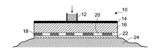
Fig. 3 shows a skin treatment device 10 which is an
embodiment of the present invention applied to a skin surface
24. The device 10 has a microwave feed connector 12 through
.which energy e.g. AC power having a predetermined stable
frequency is provided to the device from an energy source (not
shown). The feed connector may be any suitable type, e.g. a
coaxial connection such as SMA, SMB, SMC, MCX or SMP. A
grounded conductive layer 14 (e.g. of copper, silver or the
CA 02708250 2010-06-07
WO 2008/068485 PCT/GB2007/004660
like) is mounted on the dielectric substrate 16 to provided a
return current path for current supplied to a plurality of
conducting patches 18 via a feed structure (discussed below).
Each patch 18 has a rectangular shape selected so that it acts
5 as a radiating antenna for the provided microwave energy. The
shape of the radiating elements is not necessarily
rectangular, i.e. they may be square, triangular or
cylindrical. The shape may be optimised using an
electromagnetic field simulation. The plurality of patches 18
10 are arranged in a regular array, separated by air gaps 20 on
the surface of substrate 16 so that together they emit
outwardly a substantially uniform electromagnetic field. The
array of patches 18 are covered by a dielectric superstrate
22, preferably formed from a biocompatible material, e.g.
15 Parylene C, Teflon or the like.
Typically, the superstrate 22 contacts the skin 24 during
treatment. However, if more superficial treatment is required
(e.g. for tissue resurfacing), an air gap may be introduced
between the superstrate 22 and skin 24. If the distance
20 between said air gap and said tissue is such that signal
attenuation is less than 1 dB for example, then it is possible
to couple a significant portion of the source energy into the
surface of the tissue without having to place the surface of
the applicator directly in contact with the surface of the
25 tissue. The advantages of this method of treatment are: there
should be no possibility that the surface of the tissue can be
damaged in terms of burning or tissue carbonisation due to a
hot applicator, and the energy distribution may be altered by
adjustment of the stand-off distance, e.g.. by having an
30 adjustable threaded engagement between one or more dielectric
posts protruding from the device. This method can be used to
affect tissue beneath the surface of the skin, whilst leaving
the skin surface unaffected. Particular applications. may
include collagen shrinkage and the destruction of clusters of
hair follicles.
CA 02708250 2010-06-07
WO 2008/068485 PCT/GB2007/004660
31
Alternatively, a low loss dielectric block may be used
between the radiating patches and the surface of the skin. The
energy adjustment may also be made by adjusting a PIN diode
attenuator to control the power level, or by modulating a PIN
diode switch to change the pulse width or the duty cycle of
the energy delivered. Alternatively, PIN diode phase adjusters
may be used to control the phase of the radiating patches with
respect to one another. A combination of adjustment of power
level delivered to individual patches (or radiating elements)
and an adjustment in phase will enable uniform energy to be
delivered into the surface of the skin over large surface
areas when changes in the structure of the tissue - both on
the surface and below the surface - may require different
amounts of energy or different matching conditions. Thus, the
present invention may provide individually controllable
radiating elements which can adapt to variability in tissue
structure over a treatment area.
The superstrate 22 is removable, and forms the disposable
part of the apparatus.
The dielectric substrate 16 may be of any suitable
material, i.e. dielectric material preferably with a low tanb
and a relative permittivity that helps to impedance match the
device to the surface of the skin tissue being treated.
Examples of suitable materials are: PTFE, nylon, sapphire, and
alumina coated with Parylene C (where the thickness of the
coating is preferably less than 10 pm). Advantages of using
alumina include having a relative permittivity of around 10,
which is comparable to that of the skin structure, and having
good thermal conductivity. In certain instances it may be
desirable to use a material with a poor thermal conductivity
in order to prevent any heat generated by conduction from
being transferred to the surface of the tissue, which could
result in burning of the surface of the tissue, i.e. the heat
will be stored in the material rather than being conducted
into the skin.
CA 02708250 2010-06-07
WO 2008/068485 PCT/GB2007/004660
32
The relative permittivity of PTFE or nylon tends to be
relatively low, for example, between 2 and 4, thus a matching
transformer may be required between the dielectric substrate
layer and the patch antenna layer. In the instance where a low
permittivity dielectric is used, it is preferable to.sandwich
an additional dielectric layer between the dielectric
substrate layer and the patch antenna layer to perform the
necessary impedance matching and to prevent a portion of the
power being reflected at the tissue/dielectric interface.
If it is required to keep the surface of the skin cool
whilst treating diseased skin tissue, the patch antenna array
could be mounted on a Peltier cooler device. This may be of
particular interest for collagen shrinkage applications. A
ceramic substrate with good thermal conductivity may also help
to remove heat from the surface of the skin.
It may also be possible to spray the surface of the skin
with a coolant or freezer spray to cool the surface of the
tissue when the microwave energy is applied. In this
arrangement, the microwave energy is absorbed inside a layer
or layers of the skin to a depth that is related to the
frequency of the microwave energy, and the surface of the skin
is unchanged. It may be preferable to synchronise the delivery
of the coolant with the application of the microwave pulses.
For example, if the microwave pulse is of duration 100 ms, it
may be desirable to activate the spray 50 ms prior to the
pulse.
The structure illustrated in Fig. 1 is rigid and flat,
but can be modified to produce a flexible array which conforms
to irregular tissue structures. For example, Rogers
Corporation and Sheldahl (now Multek Flexible Circuits)
manufacture flexible laminate polymer circuit materials (e.g.
Rogers Corporation produce a specific material known as R/flex
3600) which may be used in implementing the present invention.
Where conducting patches 18 are used, the device design
is based on the theory of patch antenna arrays, where the size
CA 02708250 2010-06-07
WO 2008/068485 PCT/GB2007/004660
33
(length `L' and width `W') of each radiating patch is
calculated as a function of the effective dielectric constant,
which depends on the frequency of operation (e.g. 14.5 GHz)
and the dielectric constant Er of the material used to
fabricate the patch array, the dielectric constant of the skin
tissue which the patch antenna is used to treat and the
dielectric constant of the dielectric block or air gap (if
used). The superstrate 22 will also affect the performance of
the overall antenna structure and this has to be taken into
account when designing and optimising the patch antenna array.
If the thickness of the superstrate material is small, e.g. 5-
10 }im, then the effect may be negligible and can be ignored.
It is also possible to use a material that is relatively
lossy, i.e. has a tans of greater than 0.001, if only a very
thin layer is used.
The change in the effective dielectric constant due to a
thick superstrate 22 may present a substantial change, and the
amount of change is governed by the thickness and the relative
permittivity of the superstrate 22.
Table 2 provides information based on ideal calculations
performed to ascertain the number of patches per cm2 for the
dielectric loading associated with dry and wet skin with the
applicators in contact with the surface of the skin. These
figures assume that the radiating patches are in direct
contact with the skin and that the substrate material on which
the radiating patches are fabricated has no effect on the size
of the patches. It also assumes that the component of
permittivity due to the material loss is low compared to the
relative permittivity. To obtain more accurate figures and/or
take account of the factors ignored above, an electromagnetic
field simulation can be carried out to enable optimisation of
the size of the patch array or other antenna structures that
are appropriate for use with the current invention to be
performed.
CA 02708250 2010-06-07
WO 2008/068485 PCT/GB2007/004660
34
Frequency Tissue Type
GHz Wet Skin Dry Skin
Patch Patches Penetration Patch Patches Penetration
size per 10 depth (mm) size per 10 depth (mm)
L (W) mm2 L (W) mm 2
(mm) (mm)
14.5 1.93 9 2.1 2.0 9 2.16
31.0 1.16 36 0.85 1.21 25 0.82
45 0.93 49 0.61 1.0 49 0.59
Table 2: Idealised parameters associated with patch arrays
focussed into wet and dry skin tissue at
frequencies of 14.5 GHz, 31 GHz and 45 GHz.
Solid state transistor devices that operate at the above
frequencies are commercially obtainable from TriQuint
Semiconductor, Toshiba Semiconductor, Hittite Microwave
Components and Mitsubishi Semiconductor. Devices operating at
14.5GHz are becoming well established, whereas devices
operating at 31 GHz, 45 GHz, 60 GHz, 77 GHz and 94 GHz are now
beginning to become available. TriQuint Semiconductor now
manufacture 4 W devices that operate at 45 GHz and 31 GHz.
With this power output, a single device may be used to feed a
number of radiating elements. Recent developments in
semiconductor technology, particularly in PHEMT devices
provide power levels from 100 mW to 2 W to be generated at
frequencies up to 100 GHz.
The figures given in table 2 have been rounded up or
rounded down to enable complete half wavelength loaded patches
to be accommodated in a square of surface area 10 mm2. In
practical implementations, the sizes may be. slightly extended
or reduced in order to optimise the number of patches that can
be fabricated on the area of substrate material available, and
the sizes can change in accordance with results obtained from
electromagnetic field modelling. For example, if the
dimension were to be increased to 10.62 mm (W) by 10.62 mm (L)
then 16 complete half wavelength patches could be used in the
array with an operating frequency of 14.5GHz. These dimensions
CA 02708250 2010-06-07
WO 2008/068485 PCT/GB2007/004660
will change when simulations are performed since the
interaction between the lossy biological tissue structures and
the antenna structures will be taken into account. At the
simplest level, there are three values of permittivity
5 associated with the overall structure. These are:
- the complex permittivity of the biological tissue
(skin),
- the complex permittivity of the superstrate layer, and
- the complex permittivity of the substrate layer.
10 It is possible to increase the number of patches in a uniform
manner in order to increase the treatment area, for example,
at 31 GHz, 144 patches could be used to fabricate a square
treatment applicator with a surface area of 4 cm2, therefore
576 patches would be required to fabricate a square treatment
15 applicator with a surface area of 16 cm2
Fig. 4 shows a diagram of the components contained in a
complete treatment apparatus 100 according to an embodiment of
the invention. Fig. 5 shows a schematic representation of
that apparatus wherein all of the apparatus components used
20 for the microwave energy source, power feed structure and
radiating antenna array are integrated onto a single
substrate, thereby creating a compact overall design. Using
vertical stacking techniques, the apparatus 100 is made up of
a plurality of layers. A battery or AC/DC converter (i.e. a
25 power supply) 102 is mounted on a first layer 104 which
includes a user operable control and display device. The
first layer 104 is mounted on a second layer 106, which
includes a processor for the controlling the apparatus. This
layer may also contain a second processor, known as a
30 `watchdog', which is used to monitor fault conditions and act
as a means of protection in the instance that the first
processor malfunctions. The second layer 106 is mounted on a
third layer 108, which includes a microwave signal generating
line-up. The third layer 108 is mounted on a fourth layer
35 110, which includes a microwave amplifier line-up (e.g. a
CA 02708250 2010-06-07
WO 2008/068485 PCT/GB2007/004660
36
plurality of MMIC or MHEMT devices) for boosting the generated
microwave signal. The fourth layer 110 is mounted on a fifth
layer 112 which includes a feed structure (e.g. of microstrip
tracks) incorporating a network of power splitters arranged to
divide the generated microwave signal and transmit energy to
the radiating elements. The fifth layer 112 is mounted on a
sixth layer 113, which includes an array of power amplifiers
(e.g. MMIC devices) for boosting the divided signals before
they are provided to the radiating elements of the antenna
structure. The sixth layer 113 is mounted on a seventh layer
114, which includes an array of signal control devices
arranged to monitor the power delivered to and reflected from
each radiating elements and to adjust each signal e.g. to
ensure impedance matching with the tissue to be treated. The
seventh layer 114 is mounted on an eighth layer 116, which
includes an array (e.g. regular pattern) of radiating elements
(e.g. conducting patches, slot lines, or coplanar waveguide
suspended patch antennas) that each receive a divided signal
from the array of signal control devices. The eighth layer
may have a grounded conductive coating on a surface opposite
the radiating elements to provide a radiating arrangement
similar to that shown in Fig. 4. A biocompatible removable
(disposable) ninth layer 117 is provided on the eighth layer
116. The ninth layer 117 contacts the tissue to be treated
during use (i.e. it is the superstrate layer described above).
Thus, the complete apparatus can be contained within a
sandwich of layers. The main advantage of mounting the power
devices directly onto the radiating patch is that transmission
loss (or feed line loss or insertion loss) is minimised. This
is of particular interest for high frequency (e.g. 24GHz, 31
GHz, 45 GHz, 60GHz, 77 GHz, 94GHz and above) operation. It may
be desirable to split the overall. treatment system in two
separate blocks as shown in Figs 1 and 2. The first. block may
contain the microwave sub-assembly, consisting'of the
superstrate layer, the antenna array, the feed structure, the
CA 02708250 2010-06-07
WO 2008/068485 PCT/GB2007/004660
37
power generating devices and the source oscillator(s). The
second block may contain the DC power supply, the control
electronics (microprocessor and/or DSP and/or watchdog) and
the user interface.
The components in each layer are illustrated in Fig. 4.
The microwave signal is generated by a stable frequency source
126, which provides a signal at a single frequency contained
within the super high frequency (SHF) or extremely (EHF)
region of the electromagnetic spectrum and, more specifically,
at 14.5, 24, 31, 45, 66, 77, or 94 GHz (with a frequency
variation limited to a few hundred kHz). The stable frequency
source 126 shown here takes the form of a phase locked
dielectric resonator oscillator (DRO), which contains a
reference signal to which the frequency stability of microwave
source 126 is derived; the source of said reference signal
(not shown) may comprise a temperature stable crystal
oscillator, operating at a frequency in the range of between
1MHz and 100MHz, but more preferably between 10MHz and 50MHz.
Other frequency sources, such as a voltage controlled
oscillator (VCO) or a Gunn diode oscillator may be used, but
it is preferable to use a DRO in the present invention. Two
reference oscillators can be used within microwave source 126
to enhance frequency stability of the system. It may be
preferable to use a plurality of stable frequency sources to
enable a plurality of microwave frequency sources to be used
to excite a single patch antenna array. In this arrangement, a
the stable frequency source may take the form of a frequency
synthesiser.
The stable frequency source 126 is connected to the input
port of a 3dB, 0 power splitter 128. The purpose of splitter
128 is to divide the power produced by source 126 into two
equal ratios without introducing a phase change.
The first output from splitter 128 is connected to the
input of a first signal isolator 132, and the second output'
from splitter 128 is connected to the input of attenuation pad
CA 02708250 2010-06-07
WO 2008/068485 PCT/GB2007/004660
38
130. The output of attenuator pad 130 is input into a
microprocessor 124 where the signal is used to monitor the
status of the frequency source 126. The purpose of attenuator
pad 130 is to limit the signal level incident at the input to
the microprocessor 124. Should the signal indicate that
signal source 126 is functioning improperly, then
microprocessor 124 will flag up that an error has occurred and
the system will take appropriate action, i.e. an error message
will be generated, and/or the system will be shut down.
The purpose of first signal isolator 132 is to prevent
any mismatched signal present at the input of first modulation
breakthrough blocking filter 134 causing frequency changes at
source 126, due to, for example, load pulling, or another
condition that may affect the signal generated by signal
source 126. In practice, isolator 132 may not be required if
the input port of filter 134 is well matched, but isolator 132
is included as a precautionary measure. The output of first
modulation breakthrough filter 134 is connected to the input
of a modulation switch 136, whose function is to modulate the
signal produced by stable frequency source 126 to enable the
system to operate in pulsed mode, whereby the duty cycle,
pulse width, and (if wanted) pulse shape can be modified using
the user control and display unit 118 and the microprocessor
124. The purpose of the first modulation breakthrough filter
134 is to prevent frequency components contained within the
fast switching signals produced by the modulation switch 136
from getting back to the stable frequency source 126 and
affecting its output signal.
An input control signal 135 to the modulation switch 136
comes from the microprocessor 124. This control signal 135
may be a transistor-transistor logic (TTL) level signal; other
signal formats (e.g. emitter coupled logic (ECL)) are
possible.
The output from the modulation switch 136 is connected to
the input of a second modulation breakthrough blocking filter
CA 02708250 2010-06-07
WO 2008/068485 PCT/GB2007/004660
39
138, whose function is to prevent frequency components
contained within fast switching signals that may be produced
by modulation switch 136 for certain treatment modalities from
getting into the subsequent pre-amplifier 144 and power
amplifier 146 and causing, for example, signal distortion,
erroneous output power levels, or damage to these units
through, for example, the manifestation of output power stage
oscillation, or signal overdrive caused by one of the
harmonics contained within the switching signal occurring at
the same frequency as that of the signal generated by the
frequency source 126 or a signal that is within the bandwidth
of the amplifiers 144, 146, i.e. where said amplifiers provide
gain.
A practical implementation of the breakthrough blocking
filter may simply be a rectangular waveguide section, where
frequencies lower than the cut-off frequency of the waveguide
section will be blocked, hence the waveguide section acts as a
high pass filter.
The output from second modulation breakthrough blocking
filter 138 is connected to the input of a second signal
isolator 140. The output from said second isolator 140 is
connected to a variable signal attenuator 142, whose function
is to enable the system power level to be controlled by
changing the level of signal attenuation using input control
signals 143 produced by microprocessor 124. Variable signal
attenuator 142 may be an analogue or digital attenuator and
may be reflective or absorptive type. This attenuator may be
controlled by microprocessor 124 to produce a number pulse
shapes or sequences. The function of the second signal
isolator 140 is to provide isolation between the input port of
the variable attenuator 142 and the output port of the second
modulation breakthrough blocking filter 138. The second
signal isolator 140 is inserted for good design practice and
may be omitted from the apparatus without causing degradation
or damage to the microwave sub-assembly.
CA 02708250 2010-06-07
WO 2008/068485 PCT/GB2007/004660
The output from variable attenuator 142 is connected to
the input of signal pre-amplifier 144, whose function is to
amplify the signal to a level that is acceptable for driving
the input to the subsequent power amplifier stage 146. The
5 preamplifier 144 may provide a gain of between 10dB and 40dB
necessary to drive the power amplifier stage 146. The
preamplifier 144 may come in the form of a single miniature
microwave integrated circuit (MMIC), a plurality of MMICs, a
combination of MMIC(s) and discrete parts, or a plurality of
10 discrete parts. MMIC devices are preferable to discrete parts
since these devices normally produce more gain, hence a single
MMIC may be used instead of a cascade of discrete parts; this
is advantageous in terms of space (size) minimisation and heat
dissipation. For example, TriQuint's semiconductor device
15 TGA8658-EPU-SG can be used. The preferred device technology
for use in the pre-amplifier is gallium-arsenide (GaAs)
technology, although there are other emerging technologies
that may provide viable alternatives, for example, gallium
nitride (GaN) or high electron mobility transistors (HEMTs).
20 The output from pre-amplifier 144 feeds the input to
power amplifier 146, whose function is to boost the signal to
a level needed to supply the radiating antenna structure of
the treatment device.
The output from power amplifier 146 is fed to a network
25 of 3 dB power splitters 148. The power splitters 148 can be
fabricated as a microstrip structure on their respective layer
112 of the apparatus. As shown in Fig. 6, the power splitting
network comprises fifteen power splitters SPl-SP15 which divide
the signal from the power amplifier into sixteen feeds Al-A16,
30 each of which is connected.to a respective amplifier 150 in
the next layer 113. Thus, in this-embodiment the amplifier
network is fed from a single source.
Each of the sixteen amplifiers 150 is arranged so that
its output drives a conductive radiating patch or antenna 154.
35 The sixteen amplifiers 150 produce drive signals S1-S16 for this
CA 02708250 2010-06-07
WO 2008/068485 PCT/GB2007/004660
41
purpose. The amplifiers 150 each produce power at the 1 dB
compression point of 33 dBm (2W), have a gain of 16 dB and are
capable of operating in the frequency range of between 41 GHz
and 46 GHz. Suitable devices include TriQuint's semiconductor
device TGA4046-EPU.
The signals S1-S16 are fed to the conducting radiating
patches 154 on eighth layer 116 in a way that causes adjacent
patches to emit radiation orthogonally to each other.
It may be desirable to have independent control of the
microwave power supplied to each of the radiating patches so
that the overall field can be focussed (steered) in a way to
adjust for variations in the impedance of the region of tissue
being treated. This independent control is effected by the
signal control devices 152 mounted in the fifth layer 114. As
shown in Fig. 7, each signal control device comprises a front
forward directional coupler 156, a phase shifter (e.g. a PIN
diode or a varactor diode) 158, a forward power directional
coupler 160 and a reflected power directional coupler 162.
The couplers 156, 160, 162 are arranged to detect the power
travelling either in the forward direction through the device
or in the opposite direction where a signal has been reflected
from the tissue back towards the source. The signals are fed
to the microprocessor 124 via a phase and/or magnitude
detector circuit 155. The detector may take the form of a
heterodyne receiver where it is desirable to measure both
phase and magnitude information, or it may take the form of a
homodyne receiver where only magnitude information is
required. A simple diode detector may also be used where it is
only necessary to detect and.process magnitude information.
On the basis of these signals, the microprocessor (and/or DSP)
can calculate any impedance mismatch that may occur and adjust
for it by sending the necessary control signals to the phase
shifter 158.
In other words, the directional couplers 156,160,162, and
the microwave detectors or receivers(e.g. of the heterodyne,
CA 02708250 2010-06-07
WO 2008/068485 PCT/GB2007/004660
42
homodyne or diode type) measure the phase and/or magnitude of
the forward and reflected power signals. These signals are
then used to control the energy delivery profile via the phase
shifter 158. Whilst a phase shifter (e.g. PIN or varactor
diode) changes only the phase of the signals, a matching
filter, which may change both magnitude and phase can be used.
Fig. 6 shows a representation of the fifth, sixth,
seventh and eighth stacked layers 112,113,114,116 respectively
of Fig. 5, showing the feed connections between the components
on those layers. In practice, the components of adjacent
layers will be on top of one another; for clarity, Fig. 6
shows the layers in a concentric arrangement.
The arrangement shown in Fig. 6 is for a microwave energy
source to be split between sixteen conducting patches. The
fifth layer 112 has fifteen one-to-two power splitters 148
(SP1-SP15) mounted thereon in a cascading array to split the
original microwave energy source into sixteen separate sources
or signals. Thus, the original source is split into two by
one first generation splitter SP1; each of the two resulting
sources being further split into two by second generation
splitters SP2, SP3; each of those four resulting sources being
further split into two by third generation splitters SP4-SP7;
finally, each of those eight resulting sources being further
split into two by fourth generation splitters SPB-SP15. Each
output from the fourth generation splitters SPB-SP15 is fed to a
respective one of sixteen amplifiers 150 (Amp1-Amp16) in the
sixth layer 113. The amplifier outputs are then fed via
respective signal control devices 152 (C1-C16) in the seventh
layer 114 to. a respective radiating patch 154 (P1-P16) in the.
eighth layer 116. The patches 154 are square, which means
that the emitted field comes mostly from the two opposite
edges. In Fig. 6, the radiating edges 155 are indicated by
thick lines, whereas the non-radiating edges 153 are indicated
by thin lines. The feed lines are connected to the patches
154 to ensure that the radiating edges 155 of adjacent patches
CA 02708250 2010-06-07
WO 2008/068485 PCT/GB2007/004660
43
are orthogonal to one another. This may maximise the field
uniformity produced over the area of the radiating antenna
array, which, in turn, maximises the chances of being able to
produce uniform tissue effect over the area of the antenna
array.
In practice, feed line losses may need to be taken into
account in the structure shown in Fig. 6. In particular,
buffer or booster amplifiers may need to be included to
maintain a suitable signal level through the device. Each
power splitter 148 typically has a loss of 3 dB associated
with it. At 45 GHz, a feed line loss between components of up
to 7 dB is possible, which would lead to an overall loss of up
to 10 dB along each path (microstrip line) of the power
splitter cascade. This loss can be compensated for by placing
a buffer amplifier before every or every other power splitter.
The actual configuration depends on the power budget
calculated for a device. An example of a power budget is
described with respect to Fig. 20 below.
One important feature of the present invention is the
means by which power is transferred from the energy source to
the radiating elements. Each patch antenna contained within
the patch array has to be fed with microwave energy.
Generally speaking, there are two main feed structures:
parallel feed and series feed.
The parallel feed has a single input port and multiple
feed lines are connected in parallel to constitute the output
ports. Each of the feed lines is terminated at an individual
radiating element (or patch).
The series feed consists of a continuous transmission
line from which small portions of energy are progressively
coupled into individual elements disposed along the line by
various means, including proximity coupling, direct coupling,
probe coupling, or aperture coupling. The series feed
constitutes a travelling wave array if the feed line is
CA 02708250 2010-06-07
WO 2008/068485 PCT/GB2007/004660
44
terminated in a matched load, or a resonant array if it is
terminated in an open circuit or a short circuit.
One example of a series feed is a radiating transmission
line or a `leaky feeder', which may consist of a transmission
line that carries a travelling wave with a set of radiating
elements. Each element would radiate only a small fraction of
the total power, and by adjusting the size of each element
progressively along the line, a near uniform power intensity
versus length would be achievable. In this instance, the
elements are not in phase as required for a conventional far
field antenna, but this should not be of importance in this
application. In this arrangement, the impedance of each
radiating element must be lower than the characteristic
impedance of the transmission line, for example, the impedance
of the radiating elements may be 12.5 0 when the transmission
line feed impedance is 50 0, otherwise too much power will be
radiated by the first couple of radiating patches and the
return loss at the input will be poor (mismatch condition). It
may be preferable to vary the size of the radiating patches in
order to maintain uniform power along the radiating structure.
Possible materials that could be used for constructing the
patch antenna array are NovaClad from Sheldahl, thin copper
clad PTFE/glass from Taconic, or R/Flex liquid crystalline
polymer circuit material from Rogers Corporation.
Both parallel and series feeds can be realised as either
coplanar waveguide with the radiating elements or in a
separate transmission line layer. Feed lines laid in the same
plane as the patches will. radiate and could interfere with the
radiation emitted by the radiating patches - this may not be a
problem if the feed lines are controlled transmission lines
and radiation is forced out of the radiating patches. This.
problem may also be overcome by suspending the radiating.
patches above the feed lines, for example, a coplanar
waveguide fed suspended patch antenna array may be fabricated.
CA 02708250 2010-06-07
WO 2008/068485 PCT/GB2007/004660
When designing the feed structure for the patch array,
consideration should also be given to conductor and dielectric
losses (which are typically a function of frequency of
operation) and spurious radiation due to discontinuities such
5 as bends, junctions and transitions. These losses constitute
the overall insertion loss of the feed and are an important
determining factor when considering the maximum possible power
that can be delivered to each radiating patch. In the design
of these feed structures, realisable high characteristic
10 impedance feed lines, for example 200 Q, may be used to
minimise feed-line degradation. The number of divider stages
should be kept to a minimum to reduce insertion loss or feed
line loss and optimisation complexity.
Figs. 8 and 9(a), 9(b) and 9(c) show skin treatment
15 devices that are based on a slotted antenna arrangement. In
Fig. 8 the slots increase in width along the,feed line. This
is a proven method of ensuring that the same amount of
microwave energy is emitted from each slot, and provides a
viable application for sub-dermal treatment or skin
20 rejuvenation or resurfacing. The structure comprises an array
of slots formed in (e.g. cut into) the ground plane.
Microstrip lines are fabricated onto a substrate layer whereby
the lines (not shown in Fig. 8) go across the slots. An
advantage of this structure is that it is relatively easy to
25 fabricate feed lines on top of the substrate. Electromagnetic
field simulation tools are used to optimise the structure in
terms of slot spacing and slot size since the relationship
between slot size.(length) and distance from the microwave
energy feed (source) to the slot is not usually linear. It
30 has been discovered that the length of the distal slots (those
furthest away from the source) found in theory need to be
increased in order to take account of the. power reduction near
the end of the transmission line. Empirical experiments may
also be used to optimise the arrangement in an iterative
35 manner.
CA 02708250 2010-06-07
WO 2008/068485 PCT/GB2007/004660
46
The device 200 in Fig. 8 includes a source oscillator
202, which can be any of a VCO, DRO, Gunn diode, SAW device or
frequency synthesiser operating at any of, or a number of, the
discrete frequencies discussed herein, e.g. 14.5, 24, 31, 45,
60, 77 or 94 GHz. The output from the source oscillator 202
is fed to an array of eight slotted antennas 215 via a feed
structure which includes an amplifier line-up. The output
from the source oscillator 202 is firstly amplified by a
primary amplifier 204 before being divided by primary and
secondary 3dB splitters 206, 208 into four signals. Each of
these signals is amplified by a secondary amplifier 210 before
being divided into two by a tertiary 3dB splitter 212. Each
of the eight resulting signals is amplified again by a
tertiary amplifier 214 before being fed to its respective
slotted antenna 215.
As shown in Fig. 8, each antenna 215 has a grounded
conductive layer 216 with slots 218 formed therein. The slots
218 increase in width along the length of the antenna 215 so
that the energy emitted from each slot is the same, and the
field from the ensemble of slots is uniform. The dimensions
of the slots may be determined by using electromagnetic field
simulations.
The structure of the slotted antennas can be further
understood with reference to the alternative arrangement shown
in Figs. 9(a), 9(b) and 9(c), where various views of an
alternative slotted antenna structure 220 are given. Fig.
9(a) shows a top view, where a plurality of microstrip feed
lines 222 are fabricated on a dielectric substrate 224. Each
line is fed with a microwave power signal from an amplifier
line-up as discussed above.
Fig. 9(b) shows the bottom (skin-facing) surface of the
device. Here a grounded conductive layer 226 is fabricated on
the dielectric substrate 224. Slots 228 (shown with equal
width for convenience) are formed in the grounded conductive
layer 226 and dielectric substrate layer 224 to expose parts
CA 02708250 2010-06-07
WO 2008/068485 PCT/GB2007/004660
47
of the microstrip feed lines 222. The structure is designed
so that the slots 228 act as radiating elements. The size of
the slots is chosen depending on the wavelength of the
radiation at the frequency of operation. Actual values may be
obtained from electromagnetic field simulations. The
thickness of the dielectric substrate 224 is chosen to be much
less that 1 wavelength. Fig. 9(c) shows a side view of the
antenna 220.
The microstrip lines 222 are preferably set up to enable
the maximum E field or the maximum H field to be radiated
through the slots and into the tissue. The lengths of the
slots is therefore around half a wavelength. When high
microwave frequencies (e.g. 31, 45, 60, 77 or 94 GHz) are
used, the slots can be positioned in close proximity to one
another, thus providing the required conditions for the
generation of uniform energy over the entire surface of the
applicator, with limited depth of penetration by microwave
radiation.
Fig. 10 shows a specific example of a feed structure that
can be used in the current invention; a corporate (parallel)
feed 35 may be used to feed a plurality of series connected
radiating patches 37. A detailed description of this
arrangement is given below. For very large arrays, the length
of the feed lines running to each of the radiating elements
may be prohibitively long, which will result in an
unacceptably high insertion loss. For example, it is possible
that at 45 GHz, the insertion loss may be several dB for a
length of only a few centimetres. In designing an effective
symmetrical corporate fed array, the following steps must be
taken:
1) Ensure that radiating patches are matched to feed
lines through appropriate dimensioning of coupling structures,
or by using quarter-wave transformers.
2) Ensure that each pair of feed lines from
neighbouring elements is connected to a T-junction, which is
CA 02708250 2010-06-07
WO 2008/068485 PCT/GB2007/004660
48
matched to the input line, if necessary through a quarter wave
transformer.
3) Repeat until the last stage is reached where the
feed line is connected to the feed point of the array.
In the corporate feed arrangement shown in Fig. 10, the
radiating patches 18 have an input impedance of 200 0 at the
edge and are connected to feed lines 45 with a characteristic
impedance of 200 Q. The feed lines 45 from neighbouring
elements are joined using a T-junction and transformed back to
a single supply line 43 (with a characteristic impedance of
200 1) using a 140 92 quarter wave transformer 44. A
transformer that has a length corresponding to an odd multiple
of a quarter of the wavelength at the frequency of interest
(i.e. its length is (2n-1)XL/4, where 2L is the loaded
wavelength and n is an integer) will also perform the same
transformation if it is assumed that the line is lossless. At
short wavelengths, it may be practically necessary to use a
line having a length greater than one quarter wavelength, i.e.
having a length equal to an odd multiple of quarter
wavelengths. The properties of the dielectric material must
be stable in order to ensure that the transmission line acts
as an impedance transformer. This feature is of particular
importance when transformers longer than X/4 are used, i.e.
3/4X or 5/4?, etc., since the desired quarter electrical
wavelength will otherwise be modified to an electrical length
that is undesirable, for example, in the worst instance, it
could end up as a multiple of a half the electrical wavelength
and provide no transformation whatsoever. In the next step,
neighbouring pairs of supply lines are then joined at another
T-junction where they are similarly transformed through a 140
S2 quarter wave transformer 42 back to a further single supply
line 41 (the characteristic impedance is 200 0). This process
is repeated so that the pair of further supply lines 41 are
joined at a last T-junction. A final transformation uses a 71
CA 02708250 2010-06-07
WO 2008/068485 PCT/GB2007/004660
49
S2 quarter wave transformer 40 to match the parallel
combination of the two 200 S2 lines (i.e. 100 Q) with an input
line 39 (characteristic impedance = 50 92) from energy source
38 used to feed the overall array. The impedance matching is
calculated using the formula, i.e. Ztrans = 'J (ZinZout) , which, in
this case, corresponds to q(50 x 100) = 71 92 for the last
junction.
Figs. 11 and 12 illustrate another specific example of a
feed structure that can be used in the present invention.
Here an array of patches (numbering 8, 16, 32, 64, 128, etc.
depending upon the size of treatment zone) is arranged so that
each patch is fed by a single MMIC amplifier. Fig. 11 shows a
perspective view of this arrangement, where a plurality of
power amplifiers 48 are mounted on an upper layer 52 of the
device. They are arranged to receive an input signal 50 from
the stable frequency energy source (not shown). Their output
signal is fed e.g. using a low loss transmission line to a
coaxial connector 54 (e.g. an SMA connector) whose outer
conductor is connected to the grounded conducting plane (not
shown) and whose inner conductor 46 is a conducting radiating
patch 18 (shown here on the superstrate 22). Fig. 12 shows a
cross-sectional view of this connection in more detail. Each
patch 18 has a coaxial connector 54 associated with it. The
outer conductor of each coaxial connector 54 terminates at the
conducting ground plane 14, whereas the inner conductor 46
penetrates the plane and passes through the substrate layer 16
to its respective patch 18. By locating the amplifiers on a
separate layer from the radiating elements, the corporate feed
network (transmission lines or the like) can likewise be
etched onto a layer other than the layer that contains the
radiating patches. This can minimise any interference between
the feed structure and the radiating patches. With good
design practice, it is possible to fabricate the feed lines on
the same side as the radiating patches even when the whole
structure is in contact with tissue, but it is preferable to
CA 02708250 2010-06-07
WO 2008/068485 PCT/GB2007/004660
keep the feed lines and the patches separate. The idea of
providing a space between the radiating patches and the tissue
is also desirable in embodiments where the feed lines are on
the same side as the radiating patch antennas. In order to
5 compensate for feed line losses that can occur when high
frequency, e.g. SHF or EHF, radiation is used, buffer or
booster amplifiers are included in the feed structure, e.g.
between one or more of the power splitters in the fifth layer
112 shown in Fig. 5.
10 TriQuint Semiconductor manufacture devices that are
suitable for use as the power amplifiers in the present
invention. In particular, TriQuint's TGA4505-EPU parts can be
used for operation over a bandwidth of between 27 GHz and 31
GHz, and produce power levels of up to 36 dBm (4 W) in
15 compression (1 dB compression point) and provide a gain of 23
dB. The dimensions of these MMIC chips are around 2.8 mm x
2.2 mm x 0.1 mm. If one device is used to feed four patches
and the length of feed lines is kept very short, power levels
of up to 1 W may be radiated from each patch. More recently,
20 amplifiers that work up to 45 GHz (e.g. TriQuint's TGA4046-
EPU) have become available; these parts can provide up to 2 W
of power. Due to recent developments and interest in mm wave
technologies and terahertz systems, energy at high microwave
and mm wave frequencies with associated small depths of
25 penetration is becoming more readily available, and so it will
be possible to produce high localised energy densities inside
the tissue using these devices.
Fig. 13 illustrates schematically an amplifier line-up
for a 4 W generator that may be used in an embodiment of the
30 present invention. The line-up comprises a suitable frequency
source 51, which may be a closed loop phased locked dielectric
resonator oscillator (DRO) using a single or a plurality of
temperature compensated crystal oscillator references, or a
temperature compensated open loop DRO. Other frequency
35 sources, such as a Gunn diode oscillator or a voltage
CA 02708250 2010-06-07
WO 2008/068485 PCT/GB2007/004660
51
controlled oscillator (VCO) can be used; the choice of
oscillator depends on the frequency being used. The output 52
of the frequency source represents a stable frequency signal
which is fed into a pre-amplifier 47 (here TriQuint's TGA4902-
EPU-SM device), which has a 1 dB compression point of 25 dBm.
In general, monolithic microwave integrated circuits (MMICs)
are suitable for use as pre-amplifiers. For frequencies up to
about 20 GHz, gallium arsenide (GaAs) based MMICs are
preferred. For frequencies beyond this and up to 100 GHz,
high electron mobility transistor (HEMT) based MMICs or
metamorphic HEMTs can be used. For example, suitable MMICs for
31 GHz and 45 GHz operation are TriQuint's TGA4902-EPU-SM and
TGA4042-EPU parts respectively. The output of the pre-
amplifier is fed into the power amplifier 48 (here TriQuint's
TGA4505-EPU MMIC device). For frequencies up to about 20 GHz,
gallium arsenide (GaAs) or gallium nitride (GaN) transistors
or MMIC devices are suitable for use as power amplifiers. For
frequencies beyond this and up to 100GHz, it may be preferable
to use high electron mobility transistor (HEMT) based devices.
Examples of suitable power MMICs for 31GHz and 45GHz operation
are TriQuint's TGA4505-EPU and TGA4046-EPU parts respectively.
Typically, the power level from the frequency source is
in the range of -10 dBm to +15 dBm, and depends on the type of
source oscillator used, which is itself governed by the
desired frequency of operation. For example, a typical DRO
oscillator may produce power in the range -5 dBm to +5 dBm.
If the power level output provided by the frequency source 51
is -5 dBm and the gain of the pre-amplifier 47 is about 18 dB,
the power level input to the power amplifier 48 is 13 dBm.
The gain of the power amplifier 48 is about 23 dB, so the
power level at the output 56 is 36 dBm (4 W). An impedance
matched corporate feed structure 57 (see description of Fig.
10 above) splits the output 56 into individual microwave power
sources for exciting the four radiating patches 18.
CA 02708250 2010-06-07
WO 2008/068485 PCT/GB2007/004660
52
Fig. 13 shows an arrangement where a single source
oscillator 51 is followed by single pre-amplifier 47 and a
single power amplifier 48 feeding a corporate distribution
network 57. Other distribution arrangements that use
corporate feed networks are also possible. Fig. 14 shows an
arrangement where a single source oscillator 51 and a single
pre-amplifier 47 are followed by a power splitter 62, which
provides an input to a plurality of power amplifiers 48, each
of which feed a single radiating patch 18. Fig. 15 shows an
arrangement where a separate source oscillator 51 and power
amplifier 48 are provided for each radiating patch.
In Fig. 15, the power input to each patch is arranged so
that the same (i.e. parallel) edges 64 on each patch radiate.
However, to improve further the uniformity of the radiated
field, it is desirable to arrange the input feeds so that the
radiating edges 64 on adjacent patches are orthogonal to one
another. Fig. 16 shows a separate source oscillator 51 and
power amplifier 48 for feeding each radiating patch 18 where
the feeds are provided on alternating edges of adjacent
patches to cause orthogonal edges 64 to radiate and thereby
ensure a more uniform field distribution, which can lead to a
uniform tissue effect. In other words, the patch array is
set-up in such a manner that the two edges of the patches that
are dominant in producing the fringing fields are alternated
between adjacent patches. Thus, in Fig. 16, adjacent patches
are fed orthogonally and each feed line is designed such that
the output fields are in phase to produce a uniform field over
the surface of the skin.
As explained above, the device is optimised e.g. using
electromagnetic field modelling to ensure the antenna
structure is impedance matched to the characteristics of the
biological tissue and that the fields inside the skin tissue
are uniform. The feed structure can also be modelled using
microwave simulation tools such as Ansoft HFSS, Flomerics
Microstripes or CST Microwave Studio .
CA 02708250 2010-06-07
WO 2008/068485 PCT/GB2007/004660
53
Electromagnetic field modelling helps in the
determination of the position of the feed lines with respect
to the patch. For example, the position of the feed line
determines the feed impedance or the impedance seen by the
radiating patch. In the instance of the co-axially fed patch,
where a wire or pin is connected to the back of the patch and
the wire or pin is inserted through the substrate or
dielectric layer, the position of the pin with respect to the
area of the patch determines the feed impedance. It is
important to ensure that the feed line is matched to the
antenna in order to minimise the level of reflected power. The
position of the feed onto the patch also determines the two
edges of the patch that radiates. Thus, in the instance
whereby it is desirable that adjacent patches radiate
orthogonal fields, the position of the feed line with respect
to the area of the patch determines this pattern.
Fig. 17 shows a practical embodiment of the arrangement
shown in Fig. 16. Sixteen conducting patches 18 are mounted
on a substrate layer 16 in a 4x4 array. Microwave energy is
delivered from an energy source feed connector 12, from where
it is delivered to each patch via a corporate feed structure
comprising a plurality of transmission lines 70,72,74,76,78.
Primary feed line 70 from feed connector 12 splits into two
secondary feed lines 72, each of which splits into two
tertiary feed lines 74, each of which split into two
quaternary feed lines 76, each of which split into two quinary
feed lines 78 (giving sixteen in total), each of which is
connected to a radiating patch 18. The transmission lines are
arranged so that adjacent patches are fed (i.e. have their
respective quinary feed line connected to) at edges 64 that
are orthogonal to one another. The feed structure is also
impedance matched as described above.
As mentioned above, a superstrate layer, e.g. a
dielectric cover, located between the radiating patches and
the surface of the skin can be used to augment uniformity of
CA 02708250 2010-06-07
WO 2008/068485 PCT/GB2007/004660
54
tissue effect by dispersing the fields and provide a
disposable element between the e.g. metallic radiating patch
array and the human tissue. This layer may also provide a
degree of thermal isolation between the radiating patch array
and the surface of the skin. It is desirable for said cover to
be a disposable item rather than having the complete patch
antenna array as a disposable item for cost reasons. The
superstrate is therefore removable from the rest of the
device, to enable it to be easily fitted by non-trained
medical personnel. For example, it may be snap-fitted into
place. It is desirable to have a close fit to prevent air
gaps from causing an impedance mismatch condition. A locking
mechanism, e.g. clips around the edge of the device may be
used to fix the superstrate in place during use.
An alternative to the above would be to provide a
conformal coating to the patch antenna array applicator using
a biocompatible material such as Parylene C or Teflon . In
this instance the complete device would form the disposable
item. It should be noted that the dielectric cover will
affect the performance of the patch antenna array applicator
to such an extent that it must be taken into account when
designing the patch antenna array. Generally speaking, a
dielectric cover will cause the resonant frequency to be
lowered. Therefore, the patches should be designed to resonate
at a slightly higher frequency than the operating frequency of
choice. When the patch array is covered with said dielectric
cover the properties that will change include: the effective
dielectric constant of the substrate material, the losses, the
Q-factor and the directive gain. Given the unusual environment
that the patch array will be operating in, the Q-factor and
the directive gain should not need to be considered in the
same manner as they would if the patch array was to be
operating in a conventional environment, i.e. as a part of a
RADAR system, or in a line of sight communications link. The
change in the effective dielectric constant due to the cover
CA 02708250 2010-06-07
WO 2008/068485 PCT/GB2007/004660
will present the greatest change, and the amount of change is
governed by the thickness and the relative permittivity of the
substrate material. The presence of the cover layer also
produces changes in the radiation pattern produced by the
5 antenna array.
It is also worthwhile noting that the superstrate layer
will help ensure an even field distribution, or uniform tissue
effect. The correct choice of dielectric constant and loss
factor (1/Q or tanb) may enable enhanced field uniformity. It
10 may be preferable to form the superstrate layer from a
plurality of materials, with different dielectric properties
to enable the wave produced by individual radiating antennas
to be slowed down by different amounts. The materials may be
varied over the surface area and the thickness (the depth) of
15 the various materials may be varied. This feature may enhance
the field uniformity produced over the surface of the
applicator (the antenna) array.
As mentioned above, the skin treatment device of the
present invention receives its power from an energy source.
20 The energy source includes a source oscillator, e.g. a voltage
controlled oscillator (VCO) or a dielectric resonator
oscillator (DRO). For frequencies above 15GHz, a DRO is
preferred; VCOs generally use LC tuned circuits, which are
typically limited to frequencies of up to 15 GHz. Other
25 devices that could be used include: Gunn diode oscillators and
Surface Acoustic Wave (SAW) oscillators. It may be preferable
to use a closed loop phased locked DRO, or a temperature
compensated open loop DRO, in order to maintain a stable
single operating frequency. It may also be preferable to drive
30 individual radiating patches or groups of radiating patches
with source oscillators operating at different frequencies,
i.e. a plurality of source oscillators may be used, where each
individual oscillator outputs a different frequency to feed a
group of radiating patches. It may be preferable to use a
35 frequency synthesiser to produce a plurality of fixed (stable)
CA 02708250 2010-06-07
WO 2008/068485 PCT/GB2007/004660
56
frequencies. One embodiment described above is based on an
operating frequency of 14.5 GHz, where semiconductor power
devices are readily available. The size (surface area that
may be treated by the device) can vary between less than 0.5
cm2 and greater than 10 cm2. Fig. 18 shows a scale view of a
patch antenna array with a treatment surface area of about 8
cm x 9 cm where the size and separation of each patch is
calculated to be suitable for radiating an electromagnetic
field at 14.5 GHz into wet skin. Other embodiments can be
designed to operate at higher frequencies (e.g. 24.GHz, 31
GHz, 45 GHz, 60GHz, 77 GHz, 94GHz or higher) which offer the
advantage of enabling more dense arrays to be formed and a
smaller depth of penetration of radiation to be achieved. At
higher frequencies (e.g. 45 GHz or above), the energy sources
(e.g. power amplifiers) may be connected directly to the
radiating elements (radiating patches) to further reduce or
minimise feed line loss. At higher frequencies, lower
penetration depths are achievable. Fig. 19 shows a scale view
of a patch antenna array with a treatment surface area of
about 6.5 cm x 6.5 cm where the size and separation of each
patch is calculated to be suitable for radiating an
electromagnetic field at 31 GHz into wet skin. Each patch is
generally separated from its adjacent neighbours by a distance
of around XL/2, where XL is the loaded wavelength. The
separation distance is therefore reduced as frequency
increases. In practice, the size of the gaps will be
calculated precisely using a computer simulation tool to
optimise the uniformity of the radiated fields and the tissue
effects.
Fig. 20 illustrates another view of the power splitter
network of the fifth layer 112. The network in Fig. 20 has
buffer amplifiers 164,166 located at selected positions
between the power splitters to ensure that the signal
amplitude remains at a suitable level (despite feed line
losses etc.) to drive the amplifiers 150 in the sixth layer
CA 02708250 2010-06-07
WO 2008/068485 PCT/GB2007/004660
57
113. The power budget for the feed structure in Fig. 20 is
explained below.
Before the input to the network of power splitters 148,
the power amplifier 146 (having a gain of 9 dB and a 1 dB
compressed power rating of 28 dBm) increases the power from
preamplifier 144 from 16 dBm to 25 dBm. This level is then
split into two equal parts using a 3 dB splitter SP1r and a
feed line with an estimated insertion loss of 7 dB, this gives
an input power of 15 dBm at the input to each of the first
buffer amplifiers 164, which have a gain of 16 dB. The first
buffer amplifiers 164 therefore produce an output power of 31
dBm. TGA4046-EPU components from TriQuint can be used as the
first buffer amplifiers. The outputs from the first buffer
amplifiers 164 are split using 3 dB splitters SP2 and SP3, and
with feed line losses taken into account, provide four
balanced outputs at a power level of 21 dBm. These output
powers are further split using 3 dB splitters SP4-SP71 to give
eight balanced outputs of 11 dBm. These output powers are then
amplified with second buffer amplifiers 166 which have a gain
of 16 dB (e.g. TGA4046-EPU devices from TriQuint
semiconductor). The output power from each buffer amplifier
166 is therefore 27 dBm, and each of these outputs is used to
feed a respective one of eight power splitters SP8-SP15.
With feed line losses taken into account, the output
power from each of the two split parts of each of the eight
splitters SP8-SP15 is 17dBm. These outputs are fed into the
input ports of the sixteen power amplifiers 150 (Amp1-Amp16) in
the seventh layer 113. Their outputs are connected directly to
the radiating patches (not shown). The devices used here are
TriQuint's TGA4046-EPU components with a gain of 16 dB and
compressed power of 33 dBm. Thus the arrangement is therefore
capable of driving 33 dBm (2W) into each of the sixteen
radiating patches to produce a range of desirable tissue
effects.
CA 02708250 2010-06-07
WO 2008/068485 PCT/GB2007/004660
58
If desired, additional buffer amplifiers could be
included between the group of two power splitters SP21 SP3 and
the four power splitters SP4-SP7. The buffer amplifiers may
then have a lower gain.
A further implementation of applicators or antenna arrays
that may be used when working at the higher end of the
frequency range, e.g. 45GHz, 60GHz or higher is discussed
below. At these frequencies, coplanar waveguide fed suspended
patch antenna array structures may be preferred. These
alternative structures may comprise of coplanar waveguide feed
lines, appropriate feeding posts and square or rectangular
radiating patches. Coplanar waveguide structures have the
ground plane and the signal line on the same surface, hence
when the radiating patch is supported with a feeding post, the
ground plane of the coplanar waveguide structure can be used
as the ground plane for the radiating patch, i.e. the air
between the underside of the radiating patch and the ground
plane forms the dielectric substrate. The coplanar waveguide
structure can be mounted on a dielectric material or substrate
with a high dielectric constant and the radiating patch
antenna sits on a layer of air. Because the radiating patch
is supported with metal posts (or metallised plastic supports)
in air, there are no dielectric losses, thus the performance
of the radiating patch antenna may be better than that of a
conventional microstrip based antenna structure where a
dielectric material is sandwiched between the radiating patch
antenna and the ground plane.
The structure described below is similar to the co-axial
feed arrangement discussed earlier, where a wire or pin is
connected to the radiating patch and said pin is fed through
the dielectric substrate material to enable an electrical
connection to be made using, for example, a direct connection
method where a microwave connector is connected directly to
the radiating patch.
CA 02708250 2010-06-07
WO 2008/068485 PCT/GB2007/004660
59
The feed post for the proposed coplanar waveguide antenna
structure acts simultaneously as a signal line and a
mechanical support for the radiating patch antenna. It is
possible to select the desired input impedance for the patch
antenna by carefully selecting the location of the feed post.
This impedance is preferably chosen such that the feed line
can be directly matched to the radiating patch antenna without
the need to use a quarter-wave impedance transformer.
Fig. 21(a) shows a coplanar waveguide structure 400 in
which a single radiating patch antenna 402 is fed via a feed
post 404. The coplanar waveguide is formed from a signal
conductor 406 separated from a pair of ground planes 408, all
on the same side and attached to the first surface of a
dielectric material 410. In this arrangement, much less field
enters the dielectric 410 when compared with a microstrip
structure in which the signal conductor is connected to the
first surface of the dielectric and the ground plane is
connected to the second surface of said dielectric.
The dielectric thickness may be great enough to ensure
that the electromagnetic fields are substantially reduced by
the time they get to the outside world, i.e. by the time they
reach the second surface of the dielectric material and
propagate into air.
Fig. 21(b) shows a variant 401 of the structure in Fig.
21(a). In this arrangement, the second surface of the
dielectric material is fully covered with a conductor 412 that
forms a further ground plane. This structure is known as a
ground-plane coplanar waveguide or a grounded coplanar
waveguide structure. The advantage of using these coplanar
waveguide feed structures over conventional microstrip feed
structures is that the coplanar structure can operate up to
and beyond 100 GHz frequencies due to the fact that connecting
the coplanar waveguide does not entail parasitic
discontinuities in the ground plane as is the case for
microstrip structures; the effect of the parasitic elements
CA 02708250 2010-06-07
WO 2008/068485 PCT/GB2007/004660
become more prevalent as the frequency of operation is
increased.
Figs. 21(a) and 21(b) show the radiating patch antenna
electrically and physically connected to the coplanar
5 waveguide feed structure using a single feeding post. A
plurality of posts may be used to support the radiating patch.
Where posts are connected between the radiating patch and the
ground plane, the material used for the posts is desirably a
low loss dielectric material. Alternatively, quarter wave
10 stubs may be used as posts between the ground plane and the
radiating patch antenna and the posts maybe positioned such
that they are electrically transparent to the microwave
signal. The length of the posts is typically less than lmm,
e.g. 0.3mm, so it is practical to use micromachining
15 technology to fabricate the structure.
Fig. 22(a) shows an arrangement 500 for a single
radiating patch antenna 502 suspended above a coplanar
waveguide feed structure using a feeding post 504. The
arrangement 500 uses a conventional coplanar waveguide
20 structure where the ground plane 506 exists only on the first
surface of the dielectric material 508.
Fig. 22(b) shows an array 510 of eight radiating patch
antennas 502, each fed using a separate feed post 504 with one
end connected to the radiating patch antenna and the other end
25 connected to the coplanar waveguide structure.
Fig. 23 shows another embodiment of this aspect of the
invention in which an array of sixteen radiating patch
antennas 602 are each connected to the signal line 604 of
coplanar waveguide structures using feeding posts 606. In Fig.
30 23, the radiating patch antennas 602 are separated into
adjacent pairs, each pair being joined together using a single
coplanar waveguide feed line respectively. In this
embodiment, the input impedance of each radiating patch
antenna 602 is 100 0. Thus, if signal lines 604 have a
35 characteristic impedance of 100 ) then the centre point 608 of
CA 02708250 2010-06-07
WO 2008/068485 PCT/GB2007/004660
61
the lines, where the energy is fed into the structure, is 50
0, i.e. the combination of two 100 0 impedances connected in
parallel. This arrangement may be advantageous in that it is
not necessary to use a quarter-wave transformer to transform
the input impedance of the radiating patch antennas to the
output impedance of the source or generator, which is normally
50 0.
The centre point 608 of each signal line 604 is connected
to one end of a planar microstrip line 610. The characteristic
impedance of the microstrip line 610 is 50 0. The other end
of the microstrip lines 610 are grouped into pairs, each pair
of microstrip lines being connected to the output port of a
power splitters 612. The power splitters 612 are 3 dB power
splitters with the input port and the two output ports
designed to accept 50 S2 microstrip lines. Drop-in microstrip
couplers can be used. The advantage of using 3 dB couplers is
that the input power incident at the input port is split
equally into two parts to enable each radiating patch antenna
602 to produce equal amounts of microwave energy. The input
port of each power splitters 612 is connected to one end of a
primary microstrip line 614. The characteristic impedance of
the primary microstrip lines 614 is 50 Q. The other end of
the primary microstrip lines 614 are grouped into pairs, each
pair being connected to the output ports of primary power
splitters 616. The primary power splitters 616 are 3 dB power
splitters, with the input port and the two output ports
designed to accept 50 0 microstrip lines. The input port of
each primary power splitters 616 is connected to the output of
a power amplifier 618 respectively. The power amplifiers 618
are preferably based on HEMT device technology, e.g.
metamorphic HEMT technology (MHEMT), and may be a single
device or an array of individual HEMT devices integrated into
one unit to provide the necessary level of power required to
produce the desired tissue effects. The input of each power
CA 02708250 2010-06-07
WO 2008/068485 PCT/GB2007/004660
62
amplifier 618 is connected to the output of a frequency source
oscillator 620. The frequency source oscillators 620 may be
Gunn diode oscillators or dielectric resonator oscillators,
although other devices that can produce a signal at the
frequency of choice may be used.
Since there are no impedance transformers in the
structure, the patch antenna array can be designed with a
minimal number of step changes in the lines that give rise to
discontinuities that may produce unwanted radiation at the
junctions or steps where the transformations take place.
The adjacent radiating patch antennas are separated by a
distance equal to 0.8X, where X is the frequency of choice.
Where additional supporting posts are used to support the
antennas, it may be preferable for the additional posts to be
placed at the E-field centre of the radiating patches and be
connected to the ground plane. Ideally, the'additional posts
do not affect the performance of the radiating antennas.
It is preferable for the lengths of the edges of the
radiating patches to be a half the wavelength at the frequency
of operation. The electric field under the radiating patches
is maximum at the first radiating edges, zero in the middle,
and maximum again at the second radiating edge. Since the
electric field is zero at the middle of the radiating patch,
supporting posts or electric shorting walls can be erected at
these locations without disturbing the field distribution
under the radiating patches. Since in the coplanar waveguide
structure the ground planes are located in the vicinity of the
signal lines, it is easier to guide the electric field. For
microstrip transmission lines, the line impedance depends
heavily on the substrate properties and it can be difficult to
implement stable lines on some microwave dielectric materials
at high microwave frequencies, especially those defined as
being within the millimetre wave range. However, for the
coplanar waveguide structure, the width of the signal line and
CA 02708250 2010-06-07
WO 2008/068485 PCT/GB2007/004660
63
the gap between the signal line and the ground plane can be
adjusted.
The above technique may also be used at lower microwave
frequencies, although the drawback is that the gap between
adjacent patches will be increased and the overall field
pattern produced may not be as uniform, hence the tissue
effects may also be less uniform.
The feeding posts (or supports) that are used to connect
the radiating patch antennas to the feed line are preferably
flexible to enable the antenna array to be conformal with the
surface of the.tissue being treated, i.e. the skin. To
implement this feature it may be desirable to make use of
flexible plastic materials that can be coated or impregnated
with a metallic material to form the conducting contact
between the radiating antennas and the feed line within the
coplanar waveguide structure. It is preferable for the
thickness of said conductive coating or layer to be equal to
at least five skin depths at the frequency of operation to
enable the majority of the microwave energy to be transported
from the feed lines to the radiating patch antennas. At the
frequencies of interest for the implementation of the current
invention the thickness will be around 1 pm when common
conductor types are used, for example, copper (Cu) or silver
(Ag); this implies that the flexibility of the non-conductive
material used to form the flexible feed posts will be
unimpaired. The ability to produce a structure that conforms
to the surface of the skin may provide an additional feature
for the current invention.
It should be noted that it may also be preferable to
suspend the radiating patches that are fed using a corporate
feed network, such as that described earlier in this
description, or another embodiment of a planar feed network,
and make use of the ability to produce an array of radiating
antenna elements that can conform or adapt to the surface of
the skin of the particular body part of the person being
CA 02708250 2010-06-07
WO 2008/068485 PCT/GB2007/004660
64
treated. In arrangements using planar structures it may not
be possible to use the idea of having the ground plane for the
radiating patch on the same surface of the dielectric material
as the signal lines, thus co-axially fed arrangements would
need to be considered, where a first pin is used to connect
the signal line and a second pin (or a plurality of additional
pins) are used to connect the ground plane of the radiating
microstrip patch to the microstrip based feed line structure.
The suspended antenna array idea may overcome problems
associated with feed line structure heating and the reduction
of the energy available at the radiating patches caused by
conventional planar feed line structures making direct contact
with the biological treatment tissue (in this case, the
surface of the skin).
Each of the suspended radiating patches may be coated
with a biocompatible material or may have a block of radiating
material attached thereto to ensure that the surface of the
skin is not exposed to conducted heat produced by the
radiating patch antennas and to assist in producing uniform
tissue effects.