Note: Descriptions are shown in the official language in which they were submitted.
CA 02708859 2010-06-10
WO 2009/077727 PCT/GB2008/004104
- 1 -
OPTICAL SENSOR
Field of the Invention
The present invention relates to an optical sensor and
more specifically to an optical sensor for measuring
pressure and/or temperature.
Background of the Invention
0
WO 99/60341 describes an optical sensor, fabricated
using conventional micromachining techniques, for measuring
changes in temperature and pressure inside a combustion
engine. The sensor comprises a slab of silicon having a
_5 recess defined in one surface by etching. A micro-
capillary, having a silica fibre fixed inside, is adhered to
the silicon slab so as to close the recess. The face of the
silica fibre and the inner surface of the recess directly
opposite the fibre serve to define a Fabry-Perot cavity.
?0 Light incident along the silica fibre is reflected within
the Fabry-Perot cavity and guided back along the silica
fibre. The reflected light creates interference fringes
whose characteristics are determined by the length of the
Fabry-Perot cavity. Changes in the external pressure cause
25 the wall of the silicon slab directly opposite the fibre to
deflect, causing a change in the length of the Fabry-Perot
cavity. This in turn creates a change in the
characteristics of the interference fringes thus registering
a change in pressure. The sensor may also be used to sense
30 changes in temperature by employing a suitably thick slab of
silicon. Changes in temperature cause the slab to expand or
CA 02708859 2010-06-10
WO 2009/077727 PCT/GB2008/004104
- 2 -
contract, which in turn results in a similar expansion or
contraction of the Fabry-Perot cavity.
Whilst the silicon sensor may be used for many
applications, the sensor is unsuitable for environments that
are at elevated temperatures. In particular, the maximum
temperature at which the silicon sensor can operate is
around 450 C. Above this temperature, the elastic
properties of silicon become unstable making any
measurements unreliable.
.0 WO 2005/098385 describes a sapphire optical sensor
sensitive to both pressure and temperature. A waveguide
formed from an optical fibre, hollow ceramic rod or metal
tube is used to interrogate the optical sensor. The
waveguide is bonded directly to the optical sensor using one
L5 of a number of bonding techniques. In one embodiment a
sapphire optical fibre is fusion bonded to the optical
sensor at temperatures between 600 C and 1500 C.
In an alternative embodiment described in WO
2005/098385, the waveguide is spaced from the optical sensor
20 by a short distance of around 3-100 pm. However, this
sensor is not suitable for use at elevated temperatures as
the fusion bond between the waveguide and the optical sensor
will weaken and may fail between 600 C and 1500 C.
US 2007/0013914 describes an optical fibre sensor
25 formed by bonding a sapphire membrane to the end of a
capillary tube and bonding an optical fibre within the
capillary tube so'that the end of the optical fibre and the
near (to the optical fibre) surface of the sapphire membrane
define a first optical cavity. The optical fibre may be
30 bonded with epoxy or laser welded to the capillary tube.
A second optical cavity is defined by the near and far
surfaces of the sapphire membrane and is used to obtain a
CA 02708859 2010-06-10
WO 2009/077727 PCT/GB2008/004104
3 -
compensating temperature measurement. However, due to
thermal mismatch between the optical fibre and capillary
tube this sensor is not suitable for use at high
temperatures.
These prior art devices are not suitable for use at
elevated temperatures or to be cycled repeatedly from low to
high temperatures without structural damage due to thermal
mismatch. Therefore, there is required an optical sensor
that overcomes these problems.
L0
Summary of the Invention
According to a first aspect of the present invention
there is provided an optical sensor comprising an optical
L5 cavity defined by a dielectric body. The optical cavity is
responsive to one or more physical environmental conditions
such as for instance, temperature and pressure. A waveguide
having a terminal end is separated from the optical cavity
and arranged so that light is coupled from the waveguide to
20 the optical cavity. In use the waveguide is maintained at a
lower temperature than that of the dielectric body so that
the optical cavity may be responsive to environments at
higher temperatures than would otherwise damage the
waveguide.
25 Preferably, the optical cavity may be a Fabry-Perot
cavity interrogated by a broadband source of radiation
emitted and collected by the waveguide.
According to a second aspect of the present invention
the optical sensor further comprises a temperature reduction
30 means for maintaining the waveguide proximal to the terminal
end at or below the first temperature. In other words, the
temperature reduction means allows the optical sensor to
CA 02708859 2010-06-10
WO 2009/077727 PCT/GB2008/004104
4 -
operate in environments at temperatures that would otherwise
damage the optical coupling between the waveguide and
optical cavity. This damage may for instance, soften or
melt the waveguide or other optical components or mechanical
joints. This allows the waveguide to be kept close enough
to the optical cavity such that misalignment of a beam
emitted from the waveguide on to the optical cavity is
reduced. This allows the optical sensor to measure
environments at higher temperatures or higher temperature
.0 cycling than would otherwise damage the waveguide or optical-
coupling.
Preferably, the temperature reduction means may be
arranged to draw heat away from the waveguide.
Preferably, the optical sensor may further comprise a
L5 housing having a proximal end and a distal end and arranged
to support the dielectric body at the proximal end and
support the waveguide at the distal end.
Optionally, the temperature reduction means may
comprise a tube surrounding the waveguide. When placed in a
20 temperature gradient through for instance, an engine casing,
the distal end may be cooler than the proximal end and any
excess heat is drawn away from the waveguide by the
temperature reduction means. The tube may have any suitable
cross section including circular and may fit loosely or
25 snugly around the waveguide.
Preferably, the temperature reduction means may be
formed of metal, such as for instance copper or another
suitable heat conductive metal.
In accordance with a third aspect of the present
30 invention the terminal end of the waveguide is far enough
from the optical cavity so that the waveguide is maintained
at a temperature that does not damage it in use with the
CA 02708859 2010-06-10
WO 2009/077727 PCT/GB2008/004104
-
sensor operating a temperature at the dielectric body end
that would damage the optical coupling. When placed across
a temperature gradient the optical cavity may be placed at
the hotter end and the terminal end of the waveguide may be
5 located towards the cooler end of the sensor in use.
Preferably, the distance is greater than lmm. More
preferably the distance is greater than 10mm. More
preferably the distance is equal to or greater than 25mm.
Advantageously, the optical sensor may further comprise
0 an optical alignment mechanism for providing alignment
between the waveguide and the optical cavity. This allows
the waveguide to be separated further from the optical
cavity (at the hotter end of the sensor) and still maintain
sufficient alignment of a beam emitted from the waveguide
_5 and incident on the optical cavity.
Advantageously, the alignment mechanism may comprise a
ball joint having a ball arranged to support the waveguide
and a socket arranged to adjustably support the ball.
Preferably, the ball joint may be arranged within a
20 housing. With a beam emitted and collected by the waveguide
the ball joint may be manipulated to maximise the received
signal. At a maximised position the ball may then be fixed,
in position.
Preferably, the ball may be fixed in position relative
25 to the socket by a fixture of for example, a weld.
Optionally, the waveguide and optical cavity may be
aligned by mounting the waveguide off axis within a mount.
The waveguide may be rotated until the signal is maximised
and fixed in position when a maximum signal is achieved.
30 Advantageously, the optical sensor may further comprise
a collimator for collimating the light emitted from the
waveguide. This increases the useable amount of light
CA 02708859 2010-06-10
WO 2009/077727 PCT/GB2008/004104
6 -
emitted from the waveguide and further allows an increase in
distance between the optical sensor and the waveguide. A
collimated beam allows the separation between waveguide and
optical cavity to be greater than 0.5mm. Without a
collimator at greater separations alignment becomes very
difficult.
Preferably, the collimator may comprise a lens attached
to the terminal end of the waveguide by an attachment.
Attaching a lens to the end of the waveguide allows the
L0 alignment mechanism to align the lens and waveguide
simultaneously.
Optionally, the attachment may be a fusion bond between
the waveguide and the lens. Fusing the waveguide to the
lens provides a stronger attachment and allows the fibre to
be physically supported at a single point within the optical
sensor, i.e. the fusion bond between the terminal end of the
waveguide and the lens. Fusion bonding also provides
greater thermal resilience and may reduce optical losses at
the interface between waveguide and lens.
Optionally, the lens may comprise a first surface
including a curved portion surrounded by a planar portion.
Advantageously, the lens may further comprise a planar
second surface parallel with the planar portion of the first
surface.
Optionally, the curved portion or portions may be
formed by micro-machining. The lens may also take the form
of a fresnel lens or diffractive lens. These or other lens
forms may be made by etching.
Optionally, the lens may be formed from sapphire or
silica. Bonding between a silica lens and a silica fibre
(where used) is therefore simplified and more
straightforward.
CA 02708859 2010-06-10
WO 2009/077727 PCT/GB2008/004104
7 _
Optionally, the optical sensor may further comprise a
spacer extending from the dielectric body towards the
terminal end of the waveguide and surround the light emitted
from the waveguide. The dielectric body may be bonded to
the spacer, which may be a hollow tube or a solid rod
transparent to the beam emitted from the waveguide. A
hollow tube may reduce heat conduction from the hotter end
of the optical sensor to the cooler end. A solid rod may
reduce complexity of the optical sensor and reduce residual
_0 stresses. The bonding technique used may preferably
withstand the high temperatures encountered. Suitable
bonding techniques included for instance, thermocompression
bonding, eutectic flux bonding using materials such as
Yttria (see US 6,012,303), laser welding or laser assisted
L5 bonding. A thermal compression seal may reduce stresses on
the spacer during temperature cycling of the optical sensor.
Preferably, any stresses in the spacer may be removed
before and after bonding.
Optionally, the spacer may be sapphire, silica,
20 magnesium oxide, MgAlO, alumina, zirconia or other similar
materials. Preferably, the spacer and dielectric body may
have very similar coefficients of thermal expansion (CTE) to
reduce additional stresses placed on each component when the
sensor is heated in use. Therefore, it is advantageous to
25 form the spacer and dielectric body out of the same
material, e.g. sapphire-sapphire or MgO-MgO, for instance.
The spacer may be made from a polycrystalline phase material
(e.g. alumina) but should have a similar CTE to that of the
material used for the dielectric body.
30 Preferably, the'spacer may be bonded to a mount. The
mount may be integral with a housing.
CA 02708859 2010-06-10
WO 2009/077727 PCT/GB2008/004104
8 -
Advantageously, the mount may be kovar or similar alloy
capable of use at high temperatures without significant
thermally induced changes.
Optionally, the spacer may be bonded to the mount by
oxide bonding. Oxide bonding may provide,a hermetic seal.
Preferably, a thermalcompression seal may be arranged
to separate the spacer from a mount at an end of the spacer
distal from the dielectric body.
Advantageously, the thermalcompression seal may be a
low-creep washer such for instance, copper or platinum.
Advantageously, the washer may be formed from an oxidation
resistant ductile material or metal such as platinum or
gold, for instance.
Preferably, the washer may be grain-stabilised to
further reduce creep. Such washers may apply sufficient
compression over a wide temperature range and be able to
absorb stresses due to thermal mismatch, which may otherwise
shatter the spacer. In this way the spacer may be held
using a low modulus material in compression over a large
temperature range and cycle.
Preferably, where a .sapphire spacer is used, the axis
along the` sapphire spacer may be collinear with the sapphire
C-axis, i.e. its axis of zero birefringence. An advantage
of the use of the C-axis is that the optic axis of sapphire
coincides with the C-axis so the effect of birefringence is
reduced. Consideration of crystal lattice orientation
improves thermal matching. Therefore, it is preferable that
the axis of the sapphire spacer matches that of the sensor
pill. Other orientations may be possible from a mechanical
point of view so long as birefringence is considered.
Advantageously,.the spacer may be thermally and/or
mechanically isolated from the housing. This may reduce
CA 02708859 2010-06-10
WO 2009/077727 PCT/GB2008/004104
9
vibration that could interfere with the varying pressure
signal (sound).
Optionally, the spacer may further comprise a spacing
protrusion arranged to separate the spacer from the housing.
This allows a structure to be formed that has a simplified
or single mode of vibration due to a single point of
contact. Preferably, this mode may be chosen or designed to
be away from any particular frequencies of interest for the
device (e.g. typical frequencies generated by an engine
_0 being monitored). The natural or resonant frequency of this
vibration mode may then be damped without affecting the
desired sensitivity of the device over a particular
frequency range.
Optionally, the spacing protrusion may be an annular
L5 protrusion.
Preferably, the spacing protrusion may be integral with
the spacer.
Advantageously, the spacing protrusion may be separated
from the proximal end of the housing. This may further
20 reduce heat conduction to the fibre or lens arrangement.
Advantageously, the waveguide is maintainable below
about 700 C and the dielectric body may be maintainable
above about 1000 C. Suitable applications for this optical
sensor include sampling pressure and/or temperature within a
25 gas turbine or jet engine.
Preferably, the optical cavity in the dielectric body
may define at one end a membrane deflectable in response to
changes in external pressure. Absolute and instantaneous
pressure may be monitored by the optical sensor.
30 Optionally, the membrane may be concave in the
direction facing the terminal end of the waveguide. In this
CA 02708859 2010-06-10
WO 2009/077727 PCT/GB2008/004104
- 10 -
configuration the optical sensor may be less sensitive to
misalignment of the beam emitted from the waveguide.
Optionally, the dielectric body may further comprise
one or more pressure equalising channels communicating
between the interior and exterior of the optical cavity.
This reduces the pressure difference across the membrane
allowing a thinner and more deflectable membrane. Such a
sensor may also be more sensitive to small changes in
pressure waves such as sound waves.
_0 Preferably, the waveguide may be a single mode
waveguide and the dielectric body may be sapphire or
magnesium oxide. As mentioned above, the material of the
dielectric body should match the CTE of the spacer.
Preferably, the waveguide is formed from sapphire or
L5 silica. Similar transparent high temperature ceramics may
also be used.
According to a third aspect of the present invention
there is provided a gas turbine engine comprising an engine
casing having an inner surface, the inner surface enclosing
20 a hot gas space having an elevated internal operating
temperature, and an optical sensor disposed through an
aperture in the inner surface. The optical sensor comprises
an optical cavity defined by a dielectric body and
responsive to one or more physical environmental conditions
25 such as for instance, temperature and pressure, and a
waveguide with a terminal end optically coupled to the
optical cavity, wherein the dielectric body is exposed to
the hot gas space. The dielectric body may communicate with
the hot gas space by for instance, extending through the
30 inner surface in the engine casing into the hot gas space.
Hot gases from within the engine may alternatively be
CA 02708859 2010-06-10
WO 2009/077727 PCT/GB2008/004104
- 11 -
directed to the dielectric body, which may be place flush
with the inner surface or placed within the engine casing.
The optical sensor may also be used within other types
of engines such as, for instance within the combustion
chamber of internal combustion engines.
Preferably, the optical sensor may be arranged such
that the waveguide is maintained, in use, at a lower
temperature than the elevated internal operating temperature
by temperature reduction means. The internal operating
temperature exposed to the dielectric body would damage the
waveguide or optical coupling between the waveguide and
optical cavity. However, the temperature reduction means
maintains the waveguide at a lower temperature to avoid this
damage, whilst at the same time the dielectric body (which
can withstand such elevated temperatures) is in contact with
the hot gas space.
Advantageously, the temperature reduction means may be
arranged to draw heat away from the waveguide.
The optical sensor of the gas turbine engine according
to the third aspect of the present invention may comprise
any or all of the features of the optical sensor described
above with regards to the other aspects of the present
invention.
Optionally, a central portion of the membrane may be
thickened to reduce optical distortion of reflected light
from this thickened central portion. This reduces fringe
fading as light may be reflected from a relatively flatter
surface.
Preferably, the waveguide may be an optical fibre.
Optionally, the optical fibre may attach to 'a planar
waveguide at its terminal end. The planar waveguide may
then shine light onto the optical cavity.
CA 02708859 2010-06-10
WO 2009/077727 PCT/GB2008/004104
- 12 -
Optionally, the collimator described above may be in
the form of a taper or similar structure on the waveguide,
the planar waveguide or the optical fibre described above.
Brief description of the Figures
The present invention may be put into practice in a
number of ways and an embodiment will now be described by
way of example only and with reference to the accompanying
LO drawings, in which:
FIG. 1 shows a cross-sectional view of an optical
sensor including the temperature and pressure sensing
optical cavities, according to a first embodiment of the
present invention, given by way of example only;
FIG. 2 shows a schematic cross-sectional view of an
optical sensor according to a second embodiment of the
present invention, given by way of example only;
FIG. 3 shows a cross-sectional view of an optical
sensor according to a third embodiment of the present
invention;
FIG. 4 shows a schematic diagram of the optical
cavities of FIG. 1;
FIG. 5 shows a schematic diagram of an interferometer
including a phase modulator and light source used to
illuminate and detect light from the optical sensors of
FIGS. 1 - 3;
FIG. 5a shows a schematic diagram of an alternative
interferometer to that shown in FIG. 5;
FIG. 5b shows a schematic diagram of further
alternative interferometer to that shown in FIG. 5,
including two light sources;
CA 02708859 2010-06-10
WO 2009/077727 PCT/GB2008/004104
- 13 -
FIG. 5c shows a schematic diagram of an example
multiple interferometer interrogator used to illuminate and
detect light from the optical sensors of FIGS. 1 - 3;
FIG. 6 shows a graph of received light intensity versus
the optical path difference induced in the phase modulator
of FIG. 5 for an example optical sensor according to one
embodiment of the present invention;
FIG. 7 shows a side view of a lens and optic fibre
mount used within a fourth embodiment of the present
LO invention;
FIG. 8 shows a perspective view of the lens mount of
FIG. 7;
FIG. 9A shows a cross-sectional view of a lens and
optic fibre arrangement used within a fifth embodiment of
the present invention with hidden features shown in dotted
lines;
FIG. 9B shows a cross-sectional view along line C-C of
FIG. 9A of the lens and optic fibre arrangement of FIG. 9A;
FIG. 9C shows a partial cross-sectional view of the
lens of FIGS. 9A and 9B;
FIG. 10 shows a perspective view of a lens having a
curved portion used within a sixth embodiment of the present
invention;
FIG. 11 shows a magnified view of the curved portion of
FIG. 10;
FIG. 12 shows a perspective view of a mount supporting
the lens of FIGS. 9A-11;
FIG. 13 shows a schematic diagram of an example optical
filter arrangement used to generate the two light sources
shown in FIG. 5b;
FIG. 14a shows an end view of an alternative embodiment
to the example optical sensor of FIG. 1;
CA 02708859 2010-06-10
WO 2009/077727 PCT/GB2008/004104
- 14 -
FIG. 14b shows a side view of the optical sensor of
FIG. 14a;
FIG. 14c shows a cross-sectional view the optical
sensor of FIG. 14a; and
FIG. 14d shows a perspective view the optical sensor of
FIG. 14a.
It should be noted that the figures are illustrated for
simplicity and are not necessarily drawn to scale.
LO Detailed description of the preferred embodiments
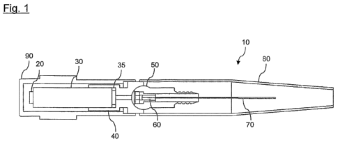
FIG. 1 shows a cross-sectional view of an optical
sensor according to a first embodiment of the present
invention. In use, a waveguide delivers a beam of light to
L5 a sensor element 20 formed from a dielectric material and
defining an optical cavity in the form of a Fabry-Perot
cavity. In the preferred embodiment the waveguide is an
optical fibre 70 but any suitable waveguide may be used.
The sensor element 20 may define one or more optical
20 cavities that may cause interference to occur in beams
reflecting off various surfaces within the sensor element
20. The reflected beams are collected by the same optical
fibre 70 used to illuminate the sensor element 20 and these
reflected beams are interrogated by an interferometer (not
25 shown in this Figure).
Pressure and/or temperature changes alter the physical
configuration of the sensor element 20 leading to changes in
the interference pattern generated and detected and these
changes in interference patterns are decoded to indicate the
30 pressure and temperature at the sensor element site. The
face of the sensor element 20 facing away from the fibre 70
,is formed from a membrane that is deflectable by changes in
CA 02708859 2010-06-10
WO 2009/077727 PCT/GB2008/004104
- 15 -
pressure. Once the membrane is deflected the dimensions , of
the optical cavity within sensor element 20 change leading
to a change in the resultant interference pattern. A
thicker layer of the material forming the sensor element 20
faces the optical fibre 70 and thermal expansion of this
thicker layer results in a change in a further optical
cavity dimension and again this leads to a change in the
interference pattern which is decoded by the detection
interferometer (not shown in this Figure).
The sensor element 20 is made from sapphire and bonded
to a sapphire spacer 30,'which'may be a solid rod or a
hollow tube. As the sensor element 20 sits at the hotter
end of the optical sensor 10 in use this bond is preferably
strong and may be formed by thermocompression, laser welding
or laser assisted bonding or any other suitable bonding
technique. Preferably this seal is hermetic to reduce the
risk of hot gasses at the sensing end of the optical sensor
from penetrating the device.
A cap 90 may be placed over the sensor element'20 to
protect it or to protect the interior of the tested
environment, such as a gas turbine engine or jet engine, for
instance. In an alternative embodiment gauze may be placed
over the cap to increase protection from foreign bodies.
A mount 40 supports the spacer and may be bonded to the
spacer by an oxide seal. To prevent damaging stresses from
occurring a compression washer 35 separates the end of the
spacer facing the optical fibre 70 from the mount 40.
Preferably the compression washer is formed from a material
to minimise creep, such as copper or platinum and grain
stabilised to further reduce creep when thermal cycling
occurs. The cap 90 may be welded to the mount 40.
CA 02708859 2010-06-10
WO 2009/077727 PCT/GB2008/004104
- 16 -
An outer sleeve 80 protects the optical sensor and
provides strain relief at the emerging end of the optical
fibre 70. The end of the optical fibre facing the sensor
element 20 incorporates a collimator. The collimator may be
a lens 60 fusion welded to the terminal end of the optical
fibre 70. The lens is secured by a collet and the collet is
secured within a ball 50 within a socket defined in a mount
40. In this way the optical fibre 70 may be secured at a
single point, i.e. the fusion weld to the lens 60, which may
be the only place that may stress the optical fibre 70. The
ball and socket arrangement allows alignment of the fibre 70
and lens 60 arrangement to be undertaken during an alignment
procedure. The lens 60 and optical fibre 70 arrangement may
be aligned to the sensor element 20 by illuminating the
sensor element 20 and monitoring the output until the signal
is maximised indicating that the optical fibre 70 and sensor
element 20 are aligned. Once alignment is achieved the ball
50 may be fixed relative to the mount 40 by a suitable
permanent technique such as e-beam or laser welding through
dedicated ports in the mount 40, for instance. Alignment of
the beam emitted from the fibre 70 to the sensor element 20
within 0.1 is desirable.
Alternatively, the optical fibre may be located off
axis and aligned by rotating the optical fibre 70 until the
signal is maximised.
A shield (not shown in this Figure) protects the free
end of, the optical fibre (70).
The sensor element 20 may be preferably manufactured
from a refractory material such as, sapphire or magnesium
oxide. These materials are transparent'in the visible and
infrared wavelength ranges, typically at least around 1300nm
and 1550nm but other wavelengths and wavelength ranges are
CA 02708859 2010-06-10
WO 2009/077727 PCT/GB2008/004104
17 -
suitable. The sensor element 20 may be produced by bonding
slices of material together. The cavity may be defined by
an etching technique such as dry etching or chemical
etching. A slice may be thinned to allow a significant
pressure response forming a pressure sensitive membrane.
The optical fibre 70 may be a single mode fibre.
As described above, a single or multiple optical
cavities may be formed in the sensor element 20. If a
single (pressure only sensing) optical cavity is required,
_0 then the surfaces of the optical sensor 20 not forming the
cavity may be wedged to frustrate any further cavities.
This provides a simplified device as only one optical cavity
needs to be interrogated. A suitable wedge angle for the
front surface of the sensor element 20 may be 5 , for
L5 instance. Such wedging also avoids coupling of unwanted
reflections where contaminants such as soot deposits, for
instance, change the reflectivity of exposed optical
surfaces.
FIG. 2 shows a schematic diagram of a second embodiment
20 of the present invention. This is a simplified diagram and
not all components are shown. In this embodiment the.
optical fibre 70 is held close to the optical sensor 20
towards the hotter end of the outer sleeve 80. In this
alternative configuration, the alignment tolerance between
25 the beam emitted from the optical fibre 70 and the optical
cavity 200 is reduced as they are spatially nearer to each
other. The minimum separation depends on thermal
considerations, i.e. how hot the optical sensor 20 is in use
and how efficiently the optical fibre 70 may be cooled.
30 Evacuating the interior of the device further reduces heat
transfer to the optical'fibre 70. For instance, this
configuration may allow the optical fibre 70 and optical
CA 02708859 2010-06-10
WO 2009/077727 PCT/GB2008/004104
- 18 -
sensor 20 to be less than or equal to about 0.5mm apart
therefore allowing satisfactory coupling without requiring a
collimator or lens. Furthermore, this embodiment does not
require such a sophisticated alignment mechanism. Instead,
the optical fibre 70 is held within a supporting tube 210,
which acts as a heat sink to draw heat away from the optical
fibre and to keep the optical fibre 70 within its optimal
temperature range. The heat sink tube 210 is attached to
the cooler end of the outer sleeve 80. In this embodiment
no collimating lens is required. Nevertheless,.a small
separation between the optical element 20 and the terminal
end of the optical fibre 70 reduces thermal contact between
those components.
Not shown in FIG. 2 is sleeving used to protect and
stress relieve the optical fibre 70 as it exits the back of
the outer sleeve 80. The method of sleeving may be
conventional but the material may preferably be capable of.
withstanding 700 C. It will be appreciated that in one
example embodiment of the present invention the sensor
design may be tailored to fit in a hole in the-side of a gas
turbine of internal combustion engine, so that the sensor
may be flush with the inner wall of the engine and is
therefore capable of measuring for example pressure. The
back end (with the optical fibre 70 exiting the optical
sensor) may be flush with the outer wall of the engine and
so the temperature gradient along the package may largely be
dictated by the heat flux in the engine wall, and the outer
engine temperature may dictate the back end temperature of
the optical sensor.
In an alternative configuration the optical sensor may,
be held at its rear end (optical fibre 70 end) so the
optical sensor may reach into a hot environment (say
CA 02708859 2010-06-10
WO 2009/077727 PCT/GB2008/004104
- 19 -
protruding into the combustion area of an engine). In this
configuration the package may have thinner walls/longer
length to allow for lower back end temperatures.
FIG. 3 shows a cross-sectional view of a third
embodiment of the present invention. Similar elements have
been given the same reference numeral as the previous
embodiments. The optical sensor 10' is similar to the
optical sensor 10 of Figure 1. Spacer tube 130 is partially
tapered at each end with the angles of taper at each end
.0 being different. Spacer 135 is a hollow tube arranged so
that the beam emitted from the optical fibre 70 passes
through the hollow section of the tube. The end of the
spacer tube 130 that the optical element 20 is attached to
is tapered with taper 135. The other end of the spacer tube
L5 130 that faces the terminal end of the optical fibre 70 is
tapered with taper 137. The angle of taper 135 to the axis
of spacer tube 130 is smaller than the corresponding angle
for taper 137.
A machined mount 40' receives the spacer tube 130 and a
20 dish shaped compression washer 35' separates the end of
spacer tube 130 from the mount 40' reducing the stresses due
to thermal expansion occurring within the spacer tube 130.
As in the first embodiment the spacer tube 130 may be made
from a refractory material such as sapphire or magnesium
25 oxide, for instance. Where sapphire is used,,the axis along
the length of the spacer tube 130 may correspond with the C-
axis of sapphire.
The spacer tube 130 is shaped so that taper 135 holds
it under compression and forms an oxide seal between the
30 aluminium oxide in the sapphire (or magnesium oxide) and the
inner surface of the mount 40'. Taper 137 and a
corresponding taper in the mount 40' have different cone
CA 02708859 2010-06-10
WO 2009/077727 PCT/GB2008/004104
- 20 -
angles to ensure alignment under compression. The angle of
taper 135 is chosen as a compromise; if it were a bigger
taper such as for instance, up to 45 there may be a high
stress concentration at the sensor element bonding area. A
smaller angle allows self locking and turns high axial
loading into smaller radial loading, which is more desirable
to provide continuous compression thereby reducing the
maximum stress seen by the spacer tube 130. The main
pressure seal is provided by the compression washer 35'.
The angle of taper 137 rear angle is about 45 as a gentle
taper here reduces the overall length.
The outer diameter of the spacer tube 130 provides a
linear alignment guide with the inner diameter of a bore
through the mount 40'. Thus the two tapers 135 and 137 may
work against each other to hold the spacer tube 130 in place
and more accurately aligned. The collimation length could
be increased further reducing the temperature of operation
of this main seal but increasing the alignment requirements.
One advantage of this design is that there is a free
space path between the optical fibre 70, which may not
survive the high temperatures that the sensor element 20 may
withstand. A suitable distance between the terminal end of
the optical fibre 70 (or its collimator) and the sensor
element 20 may be around 50-100mm. This may allow the
sensor to be used in harsh environments such as within gas
turbine engines where the temperature falls rapidly away
from the combustion zone to temperatures of the order of
600 C, which optical fibres 70 may withstand.
A cap 90' secures the spacer tube 130 and optical
element 20 assembly to'the mount 40'. A sleeve weld 125
secures the cap 90'.to the mount 40'.
CA 02708859 2010-06-10
WO 2009/077727 PCT/GB2008/004104
- 21 -
The cap 90' also prevents any internal components of
the optical sensor 10' from entering the environment to be
sensed such as, for instance, a gas turbine or jet engine or
for debris to enter or damage the sensor. A bore through
the cap 90' allows the optical element 20 to communicate
with the environment to be sensed. The inner surface of
this bore may be angled by around less than 1 to the normal
of the axis of the optical sensor 10' to reduce reflections
from the cap being fed back into the sensor.
0 In this embodiment the sleeve is welded by weld 145 to
the mount 40'. As with the first embodiment a ball joint
alignment mechanism allows the optical fibre 70 and lens 60
assembly to be aligned with the optical cavity 200. A
collet 165 secures the lens 60 within the ball 50.
.5 The collet 165 is a split collet and the lens 60 is
press fitted into the collet 165, which is itself a press
fit into the ball 50. The ball 50 is preferably made of
Kovar and the collet 165 of a soft metal such as copper so
thermal expansion doesn't allow the'lens 60 to become loose,
?0 as the initial loading allows for that. In practice this,
requires careful material selection and preparation to avoid
over compressing the lens'60 or it becoming loose due to
stressing the collet 165 beyond its yield point. In an
alternative embodiment, these problems are avoided by
25 pressing the lens 60 into a Kovar collet at a temperature of
several hundred degrees C higher than the temperature the
structure will see in use. Then when cool the collet and
lens may be press fitted into the ball. The inner bore of
the collet 165 may be oxidised to give a better surface for
30 the lens 60 to bear against, and to assist'retention by the
formation of a chemical bond between the silica of the lens
60 and the collet oxide.
CA 02708859 2010-06-10
WO 2009/077727 PCT/GB2008/004104
- 22 -
FIG. 4 shows a schematic cross-sectional view through
the optical element 20. The optical element 20 comprises
two parts, slab 400 and slab 420. Slab 400 is etched to
form a pit 200 leaving a thin membrane 410. Slab 420 is not
etched and is a uniform disc although other shapes are
suitable. A chlorine-based chemistry, preferably with
reactive ion etching, may be used to form the pit..
Pit 200 is defined by depth dl. The thickness of the
membrane 410 is d2 and the thickness of slab 420 is d3.
.0 Several optical cavities may be defined within sensor
element 20 by the various surfaces. Each of these optical
cavities may be a Fabry-Perot cavity. The pit 200 may be
lmm in diameter and the diameter of each slab may be 4mm.
However, other dimensions may be suitable. d3 may be
_5 >200pm, d2 may be of the order of 100}im and dl may be
between 3 and 50pm. When a pressure differential is applied
across membrane 410 this membrane deflects thereby changing
dimension dl. The faces of slab 420 provide an additional
optical cavity whose dimensions change as the temperature
?0 changes due to thermal expansion. Typically, the change in
dimension for a 100pm slab of sapphire is approximately 8 x
-10m per 'C.
In an alternate embodiment both slabs may be etched to
form pits, so that when the slabs are bonded together the
25 pits may face each other to form a single cavity.
After the two slabs have been bonded together slab 400
may be polished to reduce further the thickness d2 of the
membrane. Typically for pressure differences of a few bar
upwards membrane thicknesses of 50 - 100pm may give a
30 deflection of 0.3pm for a diameter of lmm. With these
example dimensions the membrane remains substantially flat,
which limits the stress in the diaphragm and therefore
CA 02708859 2010-06-10
WO 2009/077727 PCT/GB2008/004104
- 23 -
limits the possibility of long term creep. These dimensions
also provide membrane deflections that are less than a
wavelength of near infrared light typical for available
telecom grade components (1300nm or 1550 nm) in order to
further simplify interrogation.
In an alternative embodiment membrane 410 has a thicker
boss at the centre which does not deform as much as the
remaining part of the membrane and so will remain
substantially flat during the main movement. This minimises
_0 fringe fading during interrogation. A further alternative
embodiment uses a membrane that is concave in the direction
facing the optical fibre 70. This alternative embodiment
reduces the effect of angular drift and alignment errors in
the fibre-lens assembly. The radius of concave curvature
L5 may be approximately the same as the distance between lens
60 and membrane 410. Such profiling also assists with the
focussing and collimation of the incident beam back to the
fibre 70.
The sensor element 20 may be interrogated by
20 illuminating it with light. Various sources of light may be
used. Light sources include lasers and superluminescent
laser diodes (SLD), for example. A photodetector detects
the light reflected from the sensor element 20. In this way
the sensor element 20, light source and photodetector may be
25 arranged. to form an interferometer. The intensity at the
photodetector will vary depending on the wavelength of the
light source and the lengths of the optical cavities in the
sensor element 20. In other words, interference fringes
caused by the optical cavities, may be detected by the
30 photodetector. With a fixed wavelength light source,
changes in the length of the optical cavities may be
measured by correlating the intensity of the detected light
CA 02708859 2010-06-10
WO 2009/077727 PCT/GB2008/004104
- 24 -
with a particular portion (from maximum to minimum) of an
interference fringe (assuming that the change in length
resulted in a change due to less than one fringe). As the
length in a particular optical cavity changes a sinusoidal
variation in intensity will be measured at the
photodetector, assuming no optical losses occur. For
instance, a lookup table of intensities may be generated
against cavity length in order to generate the required
correlation so the measured intensity relates to one
LO particular cavity length.
However, if a laser were used as the light source
(having a coherence length greater than the largest optical
cavity length) it may be difficult to differentiate between
the fringes caused by each optical cavity, dl, d2 and d3.
L5 Furthermore, other parasitic cavities may exist (e.g.
between the terminal end of the optical fibre 70 and the
back face of the sensor element 20) that may also contribute
further unwanted fringe patterns. The use of an SLD may
remove various fringes from the output as the coherence
20 length of the light produced by the SLD may be chosen to be
low enough to discriminate against larger cavity lengths;
.light interfering within larger optical cavities will not be
coherent and so will not caused fringes. For instance, if
dl is chosen to have a smaller optical cavity-length than d2
25 and d3, and the coherence length of the SLD was less than-d2
and d3, (but greater than dl) dl will be the only optical
cavity to give rise to interference fringes.
Coherence length in SLDs is typically proportional to
output wavelength bandwidth. It may be difficult. to obtain
30 SLDs with sufficiently low coherence length to be able to
discriminate only the smallest optical cavity length, dl,
within the sensor element 20. The coherence length of the
CA 02708859 2010-06-10
WO 2009/077727 PCT/GB2008/004104
- 25 -
incident light may then be deliberately reduced by
introducing a second SLD light source having a nominally
similar wavelength (usually within about 50 nm) to the first
SLD providing the required coherence length.
In an alternative embodiment two lasers, each having
different wavelengths, may be used as the light source.
This gives rise to two separate interference fringes for
each optical cavity. Instead of using the absolute
intensity value at the photodetector to find the optical
.0 cavity lengths a ratio of the signals at the two distinct
wavelengths may be used. This reduces errors for instance,
those due to insertion loss changes during the life of the
sensor, whether due to degradation or connector variability,
as the light from each laser will be subject to similar
L5 losses but the ratio should remain unaffected by these
losses. The photodetector should be able to discriminate
between each laser wavelength in order to measure the ratio
of signals. The use of dual lasers may require the
frustration of unwanted cavities, by for instance,
20 deliberately 'wedging' optical components to avoid unwanted
interference fringes.from arising due to parasitic optical
cavities.
In a further alternative embodiment a single laser and
a SLD having a coherence length shorter than the shortest
25 optical cavity may be used. The SLD may therefore provide a
background reflection signal, which measures the return loss
of the sensor independent of the sensor cavity length. This
measured return loss may then be used to compensate for
losses encountered by the laser light.
30 A further alternative interrogator may, be similar to
the dual laser approach but instead use dual SLDs each
providing a different central wavelength. The coherence
CA 02708859 2010-06-10
WO 2009/077727 PCT/GB2008/004104
- 26 -
length of each SLD may be carefully chosen or tuned to
particular optical cavities and exclude others, as described
above. For instance, for either or both SLDs particular
coherence lengths may be chosen, such as for instance,
dl<coherence length<d3, so that the interferometer responds
only to pressure, i.e. the dl cavity length changes as the
membrane 410 is deflected. Again, a ratio of detected
signals may be used for error compensation, as described
above.
.0 Similarly, as an alternative to the one laser-and one
SLD light source the interrogator may have two SLDs with one
of the two SLDs having such a short coherence length that it
will not provide interference fringes for any optical cavity
present (with the other SLD suitable to generate fringes).
.5 However, this short coherence length SLD may . still be
sensitive to losses due to misalignment of the sensor and
therefore provide an internal calibration for the detected
signal intensity. In other words in this configuration the
second SLD may provide a normalisation signal.
?0 As a further alternative interrogator a single SLD with
a broader bandwidth may be used with the resultant light
resolved by a spectrometer and computer.
FIG. 5 shows a schematic diagram of an alternative
interrogation system suitable to interrogate the optical
25 -sensor 20. Various interrogation methods may be used
depending on the information required from the'optical
sensor. Each optical cavity, dl, d2, d3, in the optical
sensor may yield different information. Deflection of the
membrane 410 due to pressure variations may change the
30 length of dl, for instance. Thermal expansion may change d2
and d3 and so indicate temperature. Any or all of these
optical cavities may be interrogated. This alternative
CA 02708859 2010-06-10
WO 2009/077727 PCT/GB2008/004104
27 -
interrogator may comprise 'a Mach-Zehnder interferometer 300
illuminated by a SLD 320 (having a coherence length less
than each optical cavity, dl, d2 or d3, to be interrogated)
via a single mode fibre 370 pigtailed to the SLD. It should
be noted that such an SLD would not be able to discriminate
any of the optical cavities, dl, d2 or d3 used alone but
relies instead on the Mach-Zehnder interferometer. However,
the Mach-Zehnder interferometer effectively restores
coherence in order to generate inference fringes for one or
0 more particular optical cavities. Within the Mach-Zehnder
interferometer 300 there is at least one phase modulator 310
and preferably two. Fibre 70 is coupled to the side of the
Mach-Zehnder interferometer 300 opposite the SLD 320. An
interrogator chip comprising the Mach-Zehnder interferometer
L5 300 may be constructed on any suitable integrated optics
platform, such as silicon on insulator, for instance.
Light, spectrally modified by the Mach-Zehnder and
control electronics (not shown), adjusts the signal to
correspond with the cavity length of interest in the optical
20 sensor. The light is. then fed through a 3dB coupler 350 to
the sensor head, which is shown schematically here as sensor
element 20, and a collimation lens 60. Half of-the return
light from the 3dB coupler 350 is channelled back to a
photodiode 330 and thence to the detection electronics..
25 Such an interrogator may be suitable for interrogating any
or all of the optical cavities, dl, d2 and/or d3 to obtain
pressure and/or temperature information. For instance, the
expansion or elongation of more than one optical cavity may
be used to reduce inaccuracies in temperature determination.
30' FIG. 5a shows a schematic diagram of a further
embodiment similar to the example shown in FIG. 5. However,
in this further embodiment a second photodiode 335 is tapped
CA 02708859 2010-06-10
WO 2009/077727 PCT/GB2008/004104
- 28 -
into the single mode fibre 370 using a further coupler 375.
The tap may draw off around 5% of the light (or other small
proportion). Therefore, this second photodiode 335 provides
a signal proportional to the emission of the SLD 320. This
signal may be used to cancel out any variation in the signal
obtained from the first photodiode 330 due to variations or
noise in the SLD output. For instance, the signal from the
first photodiode 330 may be divided by the signal from the
second photodiode 370 to provide a corrected signal. This
J corrected signal may provide, an improvement in performance.
FIG. 5b shows a schematic diagram of a dual SLD example
implementation. A DC power supply 600 drives the system
from an AC mains supply. However, power may be obtained
from other sources especially when the device is used to
monitor engines in vehicles (e.g. portable power sources).
A first SLD 320 and a second SLD 325 are supplied with power
using filtered drive circuits 610, 620. In this embodiment
each SLD supplies a different centre wavelength. The light
outputs from each SLD 320, 325 are combined in a beam
0 combiner 630. A small proportion (-5%) of the combined
light is tapped off from a transmitter fibre. The two
wavelengths are separated using a course wavelength division
multiplex (CWDM) demultiplexer (transmit demultiplexer 640)"
and the wavelength separated light is provided to two
25 photodiodes 335, 335' in order to provide error correction
signals A and 'B to cancel out any noise and/or intensity
output variation generated by each SLD, respectively. The
wavelength bandwidth for each SLD (or other dual or multiple
light sources) may be non-overlapping.
30 The remaining'dual wavelength signal (-95%) is directed
to the sensor head 10 (via the 3dB coupler 350), which
contains the sensor element 20 and operates as described
CA 02708859 2010-06-10
WO 2009/077727 PCT/GB2008/004104
- 29 -
previously. Reflected light is collected by the 3dB coupler
350 and demultiplexed in a CWDM receiver demultiplexer 660.
The resultant light is therefore again separated by
wavelength and sampled by receiver photodiodes 330, 330'
providing receiver signals C and D corresponding to each
wavelength. The received signals C, D are analysed using
analysis electronics 650 or a suitably configured computer
system. The analysis electronics divides the signals
according to the following scheme: C/A and D/B. This
0 division step reduces variations due to connector losses or
losses in the sensor head 10, as such losses will be similar
or the same for both wavelengths. This signal processing
also reduces amplitude fluctuations due to each SLD. To
determine where on an interference fringe the output lies,
.5 (C/A) is then divided by (D/B) to provide a corrected
signal.
Alternatively, a single SLD may be filtered to provide
two outputs or wavelengths. Such optical. filtering is shown
schematically in FIG. 13. For example, the wavelength
?0 bandwidth of SLD 320 may be approximately 30nm (x). A notch
filter 710 may selectively reflect a narrow wavelength band
of light to form a first optical signal 720 having a
bandwidth of around l3nm (y). The remaining light may pass
through the notch filter 710 to provide a second optical
25 signal 730. The two optical signals may be used as if they
originated from two sources or SLDs, as described above.
Alternatively, other optical filters may be used so
provide two narrow bands. The band width for each narrow
band may be around 15nm, for instance. These narrow bands
30 may be centred on any convenient wavelength including 1510
and 1550nm, for instance.
CA 02708859 2010-06-10
WO 2009/077727 PCT/GB2008/004104
- 30 -
Other bandwidths and wavelengths may be used as
appropriate.
In an alternative embodiment the Mach-Zehnder
interferometer 300 can be placed between the sensor and the
3 detector with the same effect.
FIG. 5c shows a schematic diagram of a three-
interferometer arrangement. Each one of the three
interferometers 301, 302, 303 is a Mach-Zehnder
interferometer tuned or nominally matched to a different one
0 of the three cavities dl, d2 or d3 of interest. A three-way
splitter 350' divides the signal for each interferometer.
Three photo diodes 330, 335, 337 are shown coupled to each
of the three Mach-Zehnder interferometers 301, 302, 303.
Alternatively, multiplexing may be used so that all three
Mach-Zehnder interferometers 301, 302, 303 may be coupled to
a single photodiode. FIG. 5c shows each Mach-Zehnder
interferometer 301, 302, 303 between the sensor element 20
and the three photodiodes 330, 335, 337. Alternatively, the
Mach-Zehnder interferometers 301, 302, 303 may instead be
?0 between the light source 320 (e.g. SLD) and the sensor
element 20.
More than three interferometers may be used in a
similar arrangement to that shown in FIG. 5c, especially to
interrogate more than three cavities. Other arrangements of
25 interferometers may be used, for instance,, where one (or
more) of a plurality of interferometers interrogates
multiple cavities whilst the remaining interferometers are
directed to a single cavity.
The method of cavity interrogation is described'in
30 "Phase-nulling fibre-optic gyro", Cahill and Udd, Opt. Lett.
Vol. 4, pp93.
CA 02708859 2010-06-10
WO 2009/077727 PCT/GB2008/004104
- 31 -
A phase shift may be applied to the Mach-Zehnder
interferometer 300 such that its spectral transmittance
exactly matches the spectrum due to the sensor element's 20
reflected signal. A small dither signal (for instance, a
triangle wave) may be applied to the phase shifter 310, then
because of the symmetry of the transfer function locally,
the resulting signal may be symmetrical, i.e. the output
from the detector at the two dithering positions may be
equal so that an error signal, being the difference between
0 them,,may have a magnitude of zero. However, where the
Mach-Zehnder interferometer 300 is not initially at a null
point then the signal at the detector generated at the two
extremes of the dither signal may be equal to each other and
their difference may give rise to a non-zero error signal.
_5 This error signal may be suitably processed to be used to
instruct a change in the Mach-Zehnder off-set phase to
minimise the error signal. The dither signal may be up to
several MHz, for instance. Therefore, changes in the
dimension dl of the optical cavity 200 occurring up to
20 several 100kHz or about 1MHz may be accommodated and
detected. In this way, acoustic measurements can be made.
A further alternative embodiment may use white light
interferometry with a two-beam interferometer as described
in US 2006/0061768. A distributed sensor such as for
25 example, .a CCD may be used although this may not be
particularly suitable for acoustic measurements.
The phase modulator 210 may be a PIN diode phase
modulator as described in WO 99/24867, WO 99/60341 and US
2005/0157305. Such a phase modulator may have associated
30 control electronics capable of establishing the path length
required to match any or all in sequence of the cavities
CA 02708859 2010-06-10
WO 2009/077727 PCT/GB2008/004104
- 32 -
presented by the sensor at a speed and resolution adequate
for high dynamic range acoustic measurements.
Alternatively, a number of Mach-Zehnder interferometers
may receive the signal from the sensor element, but each one
may be optimised for one particular cavity from the sensor,
and feed to its own photodetector and associated amplifier.
FIG. 6 shows a graph of received light intensity versus
the optical path difference induced in the phase modulator
310 for a sapphire sensor element 20 made up of a sheet of
sapphire 150pm (d3) thick with a vacuum cavity (dl).of 40pm
and final sapphire layer (which forms a membrane that
responds to pressure) of 100pm (d2).
The graph of FIG. 6 shows a minimum in response at
3521im and 960 m and a maximum at 432pm. This is due to the
phase change at reflection from going to higher index
material to a lower index. This corresponds to the path
length of the first piece of sapphire 100pm thick
(multiplied by refractive index of sapphire 1.76 and by 2
because the path is only traversed once in the Mach Zehnder
but twice in the sensor). If 2 times 40pm is added to this
value one gets 432p, and if 150p multiplied by two and by
1.76 is added to 432p one gets 96O . The detection
algorithm can either scan either side of these three values
and therefore use one Mach-Zehnder interferometer to `look'
for three different minima, or the light returning from the
sensor may be fed into three Mach-Zehnder interferometers
that each look around one of the cavity lengths (dl, d2 or
d3) and minimise the signal into their own photodetector.
Note that in this case it would not be appropriate to have a
Mach-Zehnder interferometer between the light source and the
sensor element 20.- If, for example a material with a
significant"electro optic effect was used such as lithium
CA 02708859 2010-06-10
WO 2009/077727 PCT/GB2008/004104
- 33 -
niobate then the phase change could be achieved using the
electro optic effect.
The graph of FIG. 6 shows other signals due to
parasitic cavities. However, for clarity, discussion of
these parasitic cavities is omitted.
As will be appreciated by the skilled person, details
of the above embodiment may be varied without departing from
the scope of the present invention, as defined by the
appended claims.
For example, the alignment technique may be used with
an alignment mechanism other than the ball joint device
described above.
Other suitable optical fibres for use as the waveguide,
include photonic band gap fibres or LEAF fibres, for
instance.
Lens 60 may be a GRIN lens, silica aspheric or
spherical convex or other lens suitable for use at 600-
700 C.
Optical surfaces not providing an optical cavity
surface may be anti-reflection coated by for instance, "moth
eye" or other suitable coating techniques.
The ball joint may be fixed in place after alignment by
e-beam welding or other technique that avoids distorting the
housing body due to the generation of excessive heat.
More than one lens may be included to collimate or
focus the beam emitted from the optical fibre 70. This
allows larger diameter beams that improve efficiency of
illumination and collection.
Other materials may be deposited on to the membrane 410
to increase the thermal response of the sensor. For,
instance, SIC or Si, suitably passivated with a material
such as silicon nitride, may be used. Such materials
CA 02708859 2010-06-10
WO 2009/077727 PCT/GB2008/004104
- 34 -
provide an amplified thermal effect which allows higher
temperature sensitivity further allowing less material to be
used reducing the time constant for thermal detection and
monitoring.
The geometry of the sensor may be changed to allow the
beam emitted from the optical fibre 70 to travel in the
plane of the membrane 410. This may result in an optical
path of up to several mm to be achieved for a membrane
thickness d2 of a few dam. This provides a faster
temperature sensor due to a reduction in the required mass.
The cavities of the optical element 20 may be
interrogated with a dual laser, a laser and SLD to allow
discrimination between long and short. cavities or with a
slave interferometer. with broadband light.
The components of the optical sensor may be assembled
at a suitably elevated temperature to ensure compression
over the working temperature range.
In an alternative embodiment more than one fibre may be
bonded to rear of the collimator lens to improve strength
and durability, one optical fibre carries light and the
others are for mechanical purposes.
To improve mechanical strength of the lens 60 to
optical fibre 70 joint further glass encapsulation around
this joint. may be used.
Other thermal insulation may be used to maintain the
optical fibre 70 cooler than the dielectric body, including
partial. or full vacuum or gas filling.
In an alternative embodiment the alignment mechanism
for the bonded optical fibre 70 and lens 60 assembly may
include a cylindrical spring clip arrangement as shown in
FIG. 7. A cylindrical spring clip 400 retains the lens 60'
by supporting the lens 60 around the circumference of the
CA 02708859 2010-06-10
WO 2009/077727 PCT/GB2008/004104
- 35 -
lens 60. This reduces the effect of thermal expansion on
the axial alignment of the lens 60.
FIG. 8 shows a perspective view of the spring clip 400
with the lens in place. A plurality of spring fingers 410
grip and apply a force to the circumference of the lens 60.
FIG. 9A shows a fibre-lens assembly according to a
further embodiment of the present invention. A cylindrical
substrate 510 having two parallel planar surfaces is used to
form the lens 60'. A lens surface 500 is formed as a curve
by etching or micro-machining one planar surface of the
substrate 510 so that a curved surface is formed surrounded
by a planar surface. The substrate 510 may be made from,
sapphire or glass, for instance. FIG. 9C shows an expanded
view of the lens surface 500. The lens surface 500 may be
spherical or aspheric. It may also be a positive or
negative lens. In one embodiment the radius 520 of the lens
surface 500 is 0.5mm but may be smaller. The radius of
curvature of the lens surface may be 0.25mm, for instance.
The dimensions depend on the required lens-optical sensor
separation. The circumferential portion of the cylindrical
substrate 510 provides a support surface for the lens 60'
that is normal to the optical axis of the lens 60'.
The planar surface surrounding the lens surface 500 may
then abut a corresponding surface in the end cap 90 or 90'
or other suitable portion of the mount 40 or 40'. As the
surfaces are relatively large compared with the lens surface
500 alignment of the lens may be simplified. The planar
surface surrounding the lens 60 may be urged against the end
cap 90 or 90' or mount 40 or 40' by the spring fingers 410
of the spring clip 400 applying an axial force on the lens
60, e.g. by the spring fingers 410 bending to some extent at
the point that they meet the body of the spring clip 400.
CA 02708859 2010-06-10
WO 2009/077727 PCT/GB2008/004104
- 36 -
Further accuracy in alignment of the lens 60 may be achieved
by the abutting surface of the cap 90 or 90' or mount 40 or
40' having a bore or chamfer corresponding to the extent of
the lens surface 500 such that the lens surface 500 is
received by the bore or chamfer.
A planar lens may improve the alignment of the device
as it may seat more accurately within the housing (i.e.
relative to the optical axis). The fibre 70 and lens
arrangement may then be aligned, as described above, before
being welded in place by a C02 laser, for instance. This
passive alignment technique may be extended to other lens
types including rod lenses, for instance.
FIG. 9B shows a cross-sectional view along line C-C of
FIG. 9A. The opposite planar surface of the substrate 530
(i.e. opposite the etched surface containing the curved lens
surface 500) is bonded to the optical fibre 70, as described
above with reference to FIGs. 1 and 3, to the normal of the
planar surface 530. Thermal fusion bonding or other
suitable bonding may be used. The lens surface 500 as well
as the optical fibre bonding point may be centred on each
planar surface of the substrate 530 but should at least be
opposite each other and collinear.
The cylindrical substrate 510 may be 3mm in diameter
540 and 1.5mm thick 550, for example.
FIG. 10 shows a ,perspective view of the cylindrical
substrate 510 and fibre 70 of FIGs. 9A-C'. FIG. 11 shows a
magnified view of the lens surface 500 within the etched or
micro-machined region of the substrate 510. This embodiment
allows easier handling of the lens 60' during manufacture
and alignment. Although a cylindrical substrate 510 is
shown other profile shapes such as square, rectangular and
hexagonal, for instance, may be used.
CA 02708859 2010-06-10
WO 2009/077727 PCT/GB2008/004104
- 37 -
The substrate 510 may be supported by the cylindrical
spring clip 400 as described with reference to FIGs. 7 and 8
or other suitable support or alignment mechanism. FIG. 12
shows the lens 60' and fibre 70 arrangement held by a
suitable spring clip 400 similar to that described with
reference to FIG. 8.
Alternatively, the lens may be a fresnel lens or an
array of smaller lenses (e.g. 20-50). These types of lenses
may be made more easily using lithographic and/or wafer
scale dry etching techniques where scales deeper than 20pm
are difficult to fabricate.
FIGS. 14a-d show four views of an optical sensor
according to a further embodiment. FIG. 14a is an end view,
FIG. 14b is a side view and FIG. 14c is a cross-sectional
view along the line A-A of FIG. 14b. FIG. 14d shows a
perspective view of the optical sensor. In this embodiment
an inner support tube 30 supports a sensor element 20 in a
similar manner to that described with reference to FIG. 1
(although with a hollow tube rather. than solid). Similarly,
a lens 60'has been welded to a fibre 70 to provide a
collimated beam for illuminating and collecting light from
the sensor element 20.
However, in this embodiment the inner support tube or
spacer 30 is itself spaced apart from the housing or case 40
to improve mechanical and/or temperature isolation. In this
case, such a spacing is achieved by a spacing projection in
the form of an annular projection 800 provided around. the
inner support tube (spacer) 30. This provides a single or
isolated fixing point for forming a connection between the
optical components and the outer casing or housing 40. In
other words, the optical components, including the sensor
element 20, lens 60 and fibre 70 may be substantially
CA 02708859 2010-06-10
WO 2009/077727 PCT/GB2008/004104
- 38 -
mechanically and/or thermally isolated from the outer casing
40, whilst maintaining support and environmental protection.
The inner support tube or spacer 30 is'substantially
separated from the outer casing 40 by a gap, which may be
filled with gas or other fluid or evacuated to provide
additional thermal shock protection and isolation.
This embodiment improves both thermal and mechanical
isolation of the optical components. The heat path from the
environment external to the outer casing 40 (which may be at
elevated temperatures) to these optical components is
therefore limited to this single point of contact.
Alternatively, the annulus 800 may be broken to limit the
contact area between the optical components and the outer
casing 40. In this case more than one point of contact may
be made (i.e. by several lugs or shims) yet still improving
thermal and mechanical isolation.
The spacer 30 does not experience significant
mechanical loads but provides a thermal shunt. The annulus
800 provides a symmetrical fixing point so that any
resonances may be well controlled and predicted. The
resonant frequency of the optical components within the
inner support tube 30 may be configured out of the range of
pressure frequencies or sound that the device is designed to
detect. For instance, a resonant frequency above about 9kHz
may be suitable and can be adjusted by varying the length or
mass of the inner tube or spacer 30. Tapering of-the inner
tube 30 may also damp out certain frequencies or resonances,
if necessary.
The point of contact may be set back from the sensor
element 20 end of the device, i.e. away from the hot end in
use. This may further limit the heat conduction to any
optical elements, including the fibre/lens joint.. The hot
CA 02708859 2010-06-10
WO 2009/077727 PCT/GB2008/004104
- 39 -
end may act as a thermal shunt to keep the inner optical
assembly more tied to the back end (cooler) temperature.
This embodiment may improve resilience to distortion
for instance, when the device is knocked or fixed (screwed)
into place.
In this further embodiment the fibre may be actively
aligned before being fixed in position, as described
previously.