Note: Descriptions are shown in the official language in which they were submitted.
CA 02709384 2010-06-15
Description
Method and device for treating silicon wafers
Field of application and prior art
[0001] The invention relates to a method and also a
device for treating silicon wafers, in particular for
texturing and polish-etching with etching solution.
[0002] It has been known practice hitherto to etch
away approximately 5 pm from silicon wafers using
etching solution from both sides of the silicon wafers.
It is thereby possible, firstly, to eliminate sawing
damage. Furthermore, it is possible to produce a
textured top side, which is significant for the
performance of the solar cell produced from the silicon
wafer. Furthermore, the underside should be as smooth
and lustrous as possible in order that light which has
passed through is reflected and its energy can be
utilized in the course of return travel.
Object and how it is achieved
[0003] The invention is based on the object of
providing a method mentioned in the introduction and
also a device mentioned in the introduction for
carrying out the method with which problems in the
prior art can be solved and, in particular, an
advantageous further development is possible and also
improved and efficient etching of the silicon wafers.
[0004] This object is achieved by means of a method
comprising the features of claim 1 and also a device
comprising the features of claim 10. Advantageous and
preferred embodiments of the invention are the subject
matter of the further claims and are explained in
greater detail below. Although some features of the
device are described principally in connection with the
CA 02709384 2010-06-15
2 -
method, they simultaneously serve for elucidating the
device and are generally applicable thereto.
Furthermore, the wording of the priority application DE
102007063202.0 of December 19, 2007 in the name of the
same applicant is incorporated by express reference in
the content of the present description. The wording of
the claims is incorporated by express reference in the
content of the description.
[0005] According to the invention, it is provided
that, in a first method step, the silicon wafers are
transported in a horizontal position, to be precise
along a horizontal transport path. Etching solution for
texturing is applied or sprayed on from above, for
which purpose nozzles, surge pipes or the like can be
used, which are known per se for such a purpose. From
below the silicon wafers, either no liquid at all or
only little liquid is applied to the silicon wafers or
the underside thereof in this method step. At all
events, no etching liquid is sprayed on or the like
from the underside. For this purpose, a device embodied
in a correspondingly suitable manner can have, above
the transport path, said nozzles or surge pipes or the
like for wetting the top side. Below the underside,
such nozzles or the like are not provided at all.
[0006] In a later or second method step, the silicon
wafers, in the same way or with the same orientation as
in the first method step, in a horizontal position on
the transport path, are wetted with etching solution
for polish-etching from below. Advantageously, in this
case the etching solution is actually applied
exclusively from below and also exclusively to the
underside. This is because precisely if transport
rollers or the like are used for the transport path, in
the first method step some etching solution from above
can also pass onto said transport rollers and then be
transferred to the underside of the silicon wafers by
CA 02709384 2010-06-15
3 -
the transport rollers. Since this is a manageable
amount, however, the etching effect can remain very
small here. It can even be advantageous, for example in
preparation for the second method step.
[0007] In this way, approximately 4 pm to 6 pm of
material, preferably approximately 5 pm, can be removed
in a first method step for eliminating the sawing
damage and for texturing the top side. The method
duration can here be approximately 80 to 120 seconds.
In this case, the silicon wafers are advantageously
moved in a continuous fashion or moved through a
corresponding texturing module on the transport path.
[0008] In the first method step, approximately 2 pm of
material is removed or etched away on the underside. As
a result, here as well, a portion of the sawing damage
has already been eliminated, while surface texturing,
which is undesired here, has not yet taken place
correctly. After the method step of texturing, the
silicon wafers can be rinsed, advantageously with
water.
[0009] The etching solution used for the first method
step can be a customary etching solution for texturing,
preferably comprising a mixture of HF and HNO3. In the
first method step or when the latter is carried out in
the texturing module, etching solution for texturing
can be applied in a plurality of regions successively
along the transport path. For this purpose, a plurality
of groups of nozzles or the like for spraying on the
etching solution are advantageously provided
successively, advantageously on surge pipes or the like
running transversely with respect to the transport
path. This, too, is known in principle.
[0010] The texturing module is advantageously provided
with a collecting trough below the transport path, such
CA 02709384 2010-06-15
- 4 -
that etching solution that runs away can be collected
and reused. Said rinsing of the silicon wafers after
wetting with etching solution in the first method step
in the texturing module is advantageously effected in
said texturing module, particularly advantageously at
the end thereof. A section of the texturing module can
be embodied for rinsing with water, wherein a
collecting trough is provided here separately from the
collecting trough for etching solution, for the purpose
of separating the two liquids in order that a reduced
cleaning outlay arises. The intensity of rinsing with
water on the silicon wafers, that is to say the amount
of water, can be considerably greater than that for
wetting with etching solution.
(0011] Advantageously, the silicon wafers move after
the first method step or from the texturing module
directly to the next or second method step, which takes
place in a polish-etching module. Here etching solution
for polish-etching is applied, wherein the silicon
wafers are in any event transported in a continuous
fashion on a transport path through the polish-etching
module. The silicon wafers are wetted exclusively at
their underside. This can be effected, in one instance,
by slight spraying from below. A method and also a
device in the polish-etching module in accordance with
DE 10 2005 062 528 Al, to which reference is explicitly
made, are advantageously used for this purpose. In this
case, transport rollers for the silicon wafers are for
the most part immersed in a bath containing the etching
solution for polish-etching. Upon rotation, etching
solution adheres to a top side and is then brought to
the undersides of the silicon wafers, where it performs
the polish-etching. An etching removal 3 pm to 10 pm
can thus be achieved at the underside, thereby very
good polish-etching is actually possible with a very
good result with regard to a smooth and lustrous rear
side. This method step can here last somewhat longer
CA 02709384 2010-06-15
- 5 -
than in the preceding method step, and in particular
can last approximately 200 seconds. Here as well, the
etching removal can be determined by the method
duration. The etching solution used for polish-etching
is one similar to that used during texturing, although
with a larger HNO3 proportion. The etching processes can
be carried out at room temperature, a temperature range
extending from approximately 4 C to approximately 40 C.
[0012] These and further features emerge not only from
the claims but also from the description and the
drawings, wherein the individual features can be
realized in each case by themselves or as a plurality
in the form of subcombination in an embodiment of the
invention and in other fields and can constitute
advantageous and inherently protectable embodiments for
which protection is claimed here. The subdivision of
the application into individual sections and sub-
headings do not restrict the general validity of the
statements made thereunder.
Brief description of the drawings
[0013] An exemplary embodiment of the invention is
illustrated schematically in the drawings and is
explained in greater detail below. In the drawings:
figure 1 shows a schematic illustration of a device
for texturing by spraying silicon wafers from
above, and
figure 2 shows a schematic illustration of a further
device for polish-etching silicon wafers by
wetting by means of transport rollers from
below.
CA 02709384 2010-06-15
6 -
Detailed description of the exemplary embodiment
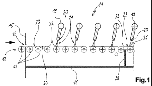
[0014] Figure 1 illustrates a texturing module 11 with
a transport path 12, which is formed by a plurality of
transport rollers 13 in a conventional manner. The
texturing module 11 has a housing 15 containing a
collecting trough 16, and from the left an inlet 18 at
the transport path 12.
[0015] Above the collecting trough 16 and the
transport path 12, a plurality of surge pipes 19 are
provided parallel to one another, which surge pipes can
run transversely with respect to the transport path 12.
They have downwardly directed nozzles 20 which output
etching solution 21. Said nozzles 20 are also known per
se to the person skilled in the art. They can be
rigidly aligned or else movable. Furthermore, the
nozzle 20 can also, under certain circumstances, be
activatable individually or in groups in order to
achieve a specific profile of the discharge of the
etching solution 21.
[0016] Silicon wafers 22 are transported on the
transport rollers 13 in a horizontal position along the
transport path 12. The top sides 23 later form the
front sides of solar cells, and the undersides 24
bearing on the transport rollers 13 form the rear sides
of said solar cells.
[0017] As can be discerned from figure 1, etching
solution 21 is discharged only onto the top sides 23 of
the silicon wafers 22. Consequently, the texturing of
the silicon wafers 22 or of the top sides 23 thereof is
principally effected here in the first method step. In
this case, it is clear, of course, that a certain
amount of etching solution 21 overflows in particular
over the front edges and their edges of the silicon
wafers 22 and is then situated on the transport rollers
CA 02709384 2010-06-15
7 -
13. Subsequent silicon wafers 22 lying on the transport
rollers 13 are then wetted with this etching solution
21 on their underside 24 as well. However, the amount
of etching solution 21 is considerably smaller here,
such that considerably less etching is effected as
well. Since, however, as is illustrated, the targeted
application of the etching solution 21 from above is
effected by means of the nozzles 20, this is referred
to as applying etching solution from above within the
meaning of the invention.
[0018] It is possible to establish whether the nozzles
are, for example, arranged above the transport
rollers 13 or oriented toward the latter, such that
15 etching solution 21 is applied to the transport
rollers 13 if there is not actually a silicon wafer 22
underneath, which intensifies the wetting of the
undersides 24 of the next silicon wafers 22 with
etching solution 21. If the nozzles 20 are arranged or
20 oriented differently, this effect is considerably
weaker. Furthermore, this effect of etching at the
underside can also be influenced by the targeted
driving of the nozzles 20 or by a targeted discharge of
the etching solution 21 onto the top sides 23 of the
silicon wafers 22.
[0019] In the texturing module 11 continued toward the
right, the nozzle 20 illustrated on the far right can
be designed not to output etching solution 21, but
rather water or rinsing water 26. Etching solution 21
can thereby be cleaned from the silicon wafer 22 in
this region for its top side 23. The separator 28 is
provided for this purpose in the collecting trough 16,
such that etching solution 21 that has dipped away is
situated to the left of said separator and the rinsing
water 26 admixed with a small proportion of etching
solution is situated to the right of said separator.
The number of successive surge pipes 19 with nozzles 20
CA 02709384 2010-06-15
8 -
for applying etching solution 21 can vary and be varied
in accordance with the desired transport speed and
method duration. Likewise, it is advantageously
possible to provide a plurality of nozzles 20 for
rinsing water 26 for rinsing the silicon wafers 22.
[0020] Figure 2 illustrates a polish-etching module
31. The latter also has a transport path 32, which is
the continuation of the transport path 12 from
figure 1. Likewise, the polish-etching module 31 is
advantageously provided and installed relatively
directly in succession with respect to the texturing
module 11. The transport path 32 is formed by transport
rollers 33. For a detailed description of the polish-
etching module 31, reference is primarily made to
DE 10 2005 062 528 Al, which describes in detail how
the etching solution 35 for polish-etching is brought
from the bath 37 to the undersides 24 of the silicon
wafers 22 by means of the transport rollers 33. They
serve, therefore, for transporting the wafers and for
wetting the underside thereof. The etching solution 35
for polish-etching is as described above. It can also
be discerned from the illustration of figure 2 that, in
the second method step, no etching solution 35
whatsoever can pass onto the top side 23 of the silicon
wafers 22, but rather only to the undersides 24.
[0021] The bath 37 has an outlet 40 between two supply
pipes 38, which introduce new etching solution 35 into
the bath 37. Said outlet, in addition to the lateral
overflow over the edge of the bath 37, ensures that
etching solution 35 is exchanged in such a way that not
only in the region of the exit of the supply pipes 38
is there fresh etching solution 35, but the latter is
also moved in the direction of the outlet 40 and,
therefore, there as well can be brought to the
undersides 24 of the silicon wafers 22 by the transport
rollers 33. In the method sequence of the treatment of
CA 02709384 2010-06-15
- 9 -
the silicon wafers 22, the polish-etching in the
polish-etching module 31 is also followed by further
rinsing, advantageously once again with water.
[0022] The polish-etching module 31 is also provided
in a housing 34. Extraction of vapors of the etching
solutions can be provided, of course, in both modules.
[0023] The substrates are typically flat, planar
silicon wafers 22 having a round contour with a
diameter of approximately 60 mm to 250 mm or a
rectangular contour with edge length of 60 mm to
250 mm. A preferred thickness lies in the range of
0.1 mm to 2 mm.