Note: Descriptions are shown in the official language in which they were submitted.
CA 02709390 2010-07-08
1
OPTICAL CONNECTOR HAVING A COMBINED PIN LOCK
AND GROUNDING MEMBER
BACKGROUND OF THE INVENTION
1. Field of the Invention
The present invention relates to optical connectors and, more
particularly, to an optical connector having a pin lock and
grounding member.
2. Brief Description of Earlier Developments
U.S. Patent 4,840,451 discloses a shielded fiber optic
connector assembly. European Patent Office patent
application No. 0927899 discloses a fiber optic connector
inserted into a metal shell of an adapter assembly. U.S.
Patent 4,818,058 discloses an optical connector having
guide rods held against Silicon blocks by a spring clip.
Electrical devices exist that generate electromagnetic
interference (EMI). These devices are shielded to
substantially prevent EMI from exiting the device and
causing interference with other electrical devices. Some
electrical devices are connected by optical conductors to
other electrical devices, such as a computer terminal
connected to a computer network by an optical cable and
connector assembly. A problem exists with connection of
conventional optical connectors to conventional electrical
devices in that an aperture is provided in the electrical
device for receiving the optical connector which results
1840959.1
CA 02709390 2010-07-08
2
in an aperture in the electrical device's shield. This can
allow EMI to escape through the optical connector aperture
in the shield. There is a need to allow optical
connectors to be connected to electrical devices, but
without also causing a substantial EMI shield breach. This
can be especially desirable for a network router having
multiple optical connector sockets; such as ten or twenty.
SUMMARY OF THE INVENTION
In accordance with the present invention, there is provided
an optical connector comprising: a housing; a shield member
located in the housing; a ferrule and optical member assembly
located, at least partially, in the housing; at least one
locating pin connected to the ferrule and optical member
assembly, the at least one locating pin extending from a
front end of the ferrule and optical member assembly; and at
least one combined pin lock and grounding member, the
combined pin lock and grounding member connecting the
locating pin to the housing and being adapted to electrically
connect a mating member, in which the optical connector is
inserted, to the shield member.
BRIEF DESCRIPTION OF THE DRAWINGS
The foregoing and other objects, advantages and features of
the present invention will become more apparent upon reading
of the following non-restrictive description of illustrative
embodiments thereof, given by way of example only with
reference to the accompanying drawings, in which:
1840959.1
CA 02709390 2010-07-08
3
Fig. 1 is a partial perspective view of an electrical and
optical component and an optical connector incorporating
features of the present invention;
Fig. 2 is a partial schematic cross-sectional view of the
optical connector shown in Fig. 1 about to be connected to a
mating member; and
Fig. 3 is a partial schematic cross-sectional view of the
optical connector and mating member shown in Fig. 2 connected
to each other.
DETAILED DESCRIPTION OF THE PREFERRED EMBODIMENT
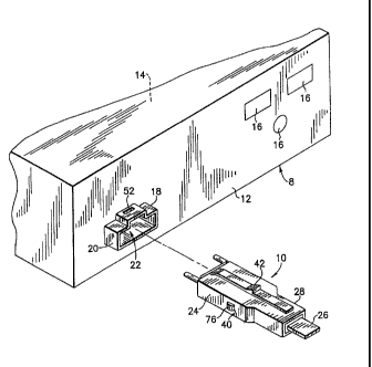
Referring to Fig. 1, there is shown a perspective view of an
electrical device 8 and an optical conductor assembly 10
incorporating features of the present invention. Although the
present invention will be described with reference to the
single embodiment shown in the drawings, it should be
understood that the present invention can be embodied in
many alternate forms of embodiments. In addition, any
suitable size, shape or type of elements or materials could
be used.
The electrical device 8 can be any suitable type of
device, such as a computer, network router or telephone. The
electrical device 8 includes a housing 12, electronic
components 14 inside the housing, electrical connectors 16,
and an optical connector socket 18. The housing 12 is
advantageously metal and forms a shield for the electronic
components 14. However, any suitable housing and shielding
could be provided. The optical connector socket 18
1840959.1
CA 02709390 2010-07-08
4
comprises a shield member 20 which is electrically connected
to the housing 12 to form part of the shield. However, an
aperture 22 exists in the shield at the socket 18; the
aperture 22 being needed to receive the plug connector 24
of the optical conductor assembly 10.
The optical conductor assembly 10 generally comprises an
optical conductor cable 26 and an optical conductor
connector 24. The optical conductor cable 26 comprises a
plurality of optical conductors, such as optical fibers
surrounded by a protective cover. However, any suitable
optical conductor cable could be used. Referring also to
Fig. 2, the optical conductor connector 24 generally
comprises a housing 28, an optical conductor and ferrule
subassembly 30, guide pins 32, a spring 34, a shield 36,
and spring members 38. The housing 28 is preferably
comprised of plastic and comprises lateral side windows 40,
a latch 42 (see Fig. 1), a spring support ledge 44,
substantially open front and rear ends 46, 48 and spring
member supports 50. The latch 42 is adapted to engage the
latch 52 at the socket 18. However, any suitable latching
arrangement could be provided. The subassembly 30 comprises
portions of the optical conductors of the cable 26, with its
cover removed, and a ferrule 54. Ferrule 54 comprises Silicon
chips locating the optical conductor portions at fixed
positions. The subassembly 30 is fixedly assembled by
suitable means, such as epoxy. Lateral sides 56 of the
ferrule 54 form guide pin receiving areas. The cable 26
extends out of the rear end 58 of the ferrule. However, in
alternate embodiments any suitable optical conductor and
ferrule subassembly could be provided. In this embodiment
1840959.1
CA 02709390 2010-07-08
the subassembly 30 is movably mounted to the housing 28 to be
able to slide relative to the housing 28. However, the
subassembly 30 need not be movably mounted to the housing or
any suitable movement could be provided.
The shield 36 is located against the rear end 58 of the
ferrule 54. The shield 36 has EMI shielding properties. In
this embodiment the shield 36 is comprised of metal and has a
general "U" shape. However, in alternate embodiments the
shield could have any suitable shape and be comprised of
any suitable material(s). The shield 36 has a front planar
section 60 which includes an aperture or slit 62. The slit
62 is about the same cross-sectional size and shape as the
cable 26. The cable 26 extends through the slit 62. The
spring 34 surrounds a portion of the cable 26 and is located
between the spring ledge 44 and the center section 60 of the
shield 36. The spring 34 biases the shield 36 in a forward
direction. Because the shield 36 is located against the rear
end 58 of the ferrule 54, the subassembly 30 is, thus,
biased by the spring in a forward direction. The shield
36 can slide rearward relative to the housing 28 if the
subassembly 30 is pushed rearward. Sides 64 of the shield
extend along the outside of the spring 34 and part of the
cable 26, and are located proximate interior surfaces of
lateral sides of the housing 28.
The spring members 38 are comprised of electrically
conductive material, such as metal. The members 38 can
perform two functions. First, the members 38 can function as
a lock or fastener for fixedly attaching the guide pins 32
to the housing 28 and against the ferrule 54. Second, the
1840959.1
CA 02709390 2010-07-08
6
members 38 can function as grounding contacts and shields.
This second function will be described in greater detail
below. Thus, each of the members 38 forms a combined pin
lock and grounding contact member. In alternate
embodiments, more of less than two members 38 could be
used. The members 38 could also perform more or less than
two functions. Each member 38 comprises a locking section
66 and a resiliently deflectable section 68. In alternate
embodiments the members 38 could have any suitable shape.
The locking section 66 comprises two projections 70 and
recesses 72. The projections 70 extend into recesses 74 in
the guide pins 32. The member supports 50 of the housing
28 extend into the recesses 72 of the members 38 during
insertion of the spring members 38 into the housing 28 to
prevent further movement of the locking section 66
relative to the housing 28. Once spring members 38 are
inserted into housing 28, the pins 32 are inserted. The
location of the projections 70 into guide pin recesses 74
stationarily fixes the guide pins 32 to the housing 28.
The locking section 66 also biases the guide pins 32 against
the lateral sides 56 of the ferrule 54 into the guide pin
receiving areas as the ferrule is inserted into the housing
28. However, the ferrule 54 its cover removed, and a ferrule
54. Ferrule 54 comprises Silicon chips locating the optical
conductor portions at fixed positions. The subassembly 30 is
fixedly assembled by suitable means, such as epoxy.
Lateral sides 56 of the ferrule 54 form guide pin receiving
areas. The cable 26 extends out of the rear end 58 of the
ferrule. However, in alternate embodiments any suitable
optical conductor and ferrule subassembly could be
1840959.1
CA 02709390 2010-07-08
7
provided. In this embodiment the subassembly 30 is movably
mounted to the housing 28 to be able to slide relative to the
housing 28. However, the subassembly 30 need not be movably
mounted to the housing or any suitable movement could be
provided.
The shield 36 is preferably located against the rear end 58
of the ferrule 54. The shield 36 has EMI shielding
properties. In this embodiment the shield 36 is comprised of
metal and has a general "U" shape. However, in alternate
embodiments the shield could have any suitable shape
and be comprised of any suitable material(s). The
shield 36 has a front planar section 60 which includes an
aperture or slit 62. The slit 62 is about the same cross-
sectional size and shape as the cable 26. The cable 26
extends through the slit 62. The spring 34 surrounds a
portion of the cable 26 and is located between the spring
ledge 44 and the center section 60 of the shield 36. The
spring 34 biases the shield 36 in a forward direction.
Because the shield 36 is located against the rear end 58 of
the ferrule 54, the subassembly 30 is, thus, biased by
the spring in a forward direction. The shield 36 can
slide rearward relative to the housing 28 if the
subassembly 30 is pushed rearward. Sides 64 of the shield
extend along the outside of the spring 34 and part of the
cable 26, and are located proximate interior surfaces of
lateral sides of the housing 28.
The spring members 38 are comprised of electrically
conductive material, such as metal. The members 38 can
perform two functions. First, the members 38 can function
1840959.1
CA 02709390 2010-07-08
8
as a lock or fastener for fixedly attaching the guide pins
32 to the housing 28 and against the ferrule 54. Second, the
members 38 can function as grounding contacts and shields.
This second function will be described in greater detail
below. Thus, each of the members 38 form a combined pin
lock and grounding contact member. In alternate
embodiments, more of less than two members 38 could be used.
The members 38 could also perform more or less than two
functions. Each member 38 comprises a locking section 66
and a resiliently deflectable section 68. In alternate
embodiments the members 38 could have any suitable shape.
The locking section 66 comprises two projections 70 and
recesses 72. The projections 70 extend into recesses 74 in
the guide pins 32. The member supports 50 of the housing
28 extend into the recesses 72 of the members 38 during
insertion of the spring members 38 into the housing 28 to
prevent further movement of the locking section 66
relative to the housing 28. Once spring members 38 are
inserted into housing 28, the pins 32 are inserted. The
location of the projections 70 into guide pin recesses 74
stationarily fixes the guide pins 32 to the housing 28.
The locking section 66 also biases the guide pins 32 against
the lateral sides 56 of the ferrule 54 into the guide pin
receiving areas as the ferrule is inserted into the housing
28. However, the ferrule 54 can slide along the guide pins
32. The deflectable section 68 includes a first portion 76
and a second portion 78. The first portion 76 extends out
of the housing 28 at one of the side windows 40. The second
portion 78 is adapted to contact the shield 36 when the first
portion 76 is pushed into the window 40.
1840959.1
CA 02709390 2010-07-08
9
Referring also to Fig. 3, the connector 24 is shown
inserted into the socket 18. When the connector 24 is
inserted, it connects to a mating connector 25 connected to
the socket 18. The socket 18 could be part of the mating
connector 25. As the connector 24 is inserted into the
socket 18, the first portions 76 of the deflectable
sections 68 contact the socket 18 and are deflected
inward back into the windows 40. The first portions 76
subsequently rest against the interior surface 80 of the
socket 18 and make electrical contact thereat. When the
first portions 76 are deflected inward, the second
portions 78 are moved into contact with the sides 64 of
the shield 36. Thus, an electrical connection is established
between the shield 36 and the socket 18 through the members
38. As noted above, the subassembly 30 and the shield 36
are slidably mounted to the housing 28. The connection of
the second portion 78 against the sides of the shield 64
allows the shield 36 to slide along the second portion 78
while still maintaining electrical connection between the
members 38 and the shield 36.
With the present invention, the optical connector 24 is able
to close a substantial portion of the gap in the shielding
of the electronic device 8 at the aperture 22. The shield 36
and members 38 cooperate with the socket 18 to form a shield
at a majority of the aperture 22 when the connector 24 is
inserted into the socket 18. This is accomplished while still
allowing the subassembly 30 to be movably mounted to the
housing 28. In addition, the members 38 can be configured
to perform multiple functions as an electrical
1840959.1
CA 02709390 2010-07-08
contact/shield, and as retainers to connect the guide pins
to the housing and bias the guide pins against the ferrule
54. This can result in a reduction of manufacturing costs
for the optical connector.
It should be understood that the foregoing description is only
illustrative of the invention. Various alternatives and
modifications can be devised by those skilled in the art
without departing from the invention. Accordingly, the
present invention is intended to embrace all such
alternatives, modifications and variances which fall within
the scope of the appended claims.
1840959.1