Note: Descriptions are shown in the official language in which they were submitted.
CA 02709511 2010-07-14
ELECTRICAL SWITCHING COMPONENT
BACKGROUND
Electrical switching devices such as relays and circuit breakers are often
encapsulated in
cases to protect the operating mechanisms from dust, moisture and other
environmental
conditions, and to prevent technicians and others from contacting live
electrical parts. Certain
operating conditions may cause a blast or build-up of hot, pressurized gases
and other materials
within the case. For example, short circuits may cause contacts in relays or
circuit breakers to
melt or explode, thereby releasing hot gases and molten metal. As another
example, an over
current condition may cause the contacts in a circuit breaker to open, which
may in turn, create a
momentary arc between the contacts. The arc releases a blast of ionized air.
If the blast is not vented from inside the case, it may damage, destroy or
interfere with the
operation of the electrical device and/or cause the case to rupture, thereby
scattering dangerous
blast products which can, in turn, cause a fire and/or create an electrical
shock hazard. Thus,
cases for electrical switching devices are often provided with a vent in the
top or side of the case
to enable a short circuit or other type of blast to escape from within the
case. While venting the
case may solve certain problems with the electrical switching device, it often
causes other
problems. For example, in an electrical enclosure housing multiple components,
a blast from
one device may be directed at another device, which in turn is damaged or
destroyed by the blast.
In addition, within the electrical switching device, the blast can short high
voltage terminals with
low voltage circuitry, creating a potential hazard.
Some other previous efforts to accommodate a blast from an electrical
switching device
have involved the use of complicated systems of baffles or dividers between
components to
direct the blast from one component away from other components. These systems,
however, add
cost and complexity, and may still create hazardous conditions.
BRIEF DESCRIPTION OF THE DRAWINGS
Fig. 1 illustrates an embodiment of a venting system for an electrical
switching
component according to the inventive principles of this patent disclosure.
1
CA 02709511 2010-07-14
Fig. 2A is a front view of another embodiment of a venting system according to
the
inventive principles of this patent disclosure.
Fig. 2B is a cross section taken through line AA of the embodiment of Fig. 2A.
Fig. 3 illustrates an embodiment of a relay according to some inventive
principles of this
patent disclosure.
Fig. 4 illustrates an embodiment of a relay card according to some inventive
principles of
this patent disclosure.
Fig. 5 is a cross-sectional view illustrating another embodiment of a venting
system
according to some inventive principles of this patent disclosure.
Fig. 6 is a cross-sectional view illustrating another embodiment of a venting
system
according to some inventive principles of this patent disclosure.
Fig. 7 is a cross-sectional view illustrating another embodiment of an
electrical switching
component according to some inventive principles of this patent disclosure.
Fig. 8 is a partially exploded perspective view illustrating another
embodiment of a
venting system according to some inventive principles of this patent
disclosure.
Fig. 9 is a perspective view showing the opposite side of the embodiment of
Fig. 8.
Fig. 10 is a perspective view illustrating an electrical switching device
according to some
inventive principles of this patent disclosure.
Fig. 11 is a cutaway view illustrating a duct according to some inventive
principles of this
patent disclosure.
Fig. 12 is a cross-sectional view illustrating an example of an interface of
the electrical
switching device and case of Fig. 11.
Fig. 13 is an exploded cutaway view of the embodiment of Fig. 11.
Fig. 14 is a cross-sectional view illustrating an example of an interface of a
wall of the
case and a wall of the electrical switching device.
Fig. 15 is a cutaway view illustrating a bulkhead according to some inventive
principles
of this patent disclosure.
Fig. 16 is an exploded cutaway view of the embodiment of Fig. 15 from a
different angle.
Fig. 17 is a cutaway view illustrating a circuit board in the assembly of Fig.
16 according
to some inventive principles of this patent disclosure.
2
CA 02709511 2010-07-14
Fig. 18 is a cutaway view illustrating a circuit board according to some
inventive
principles of this patent disclosure.
Fig. 19 is the cutaway view of Fig. 17 without the circuit board.
Fig. 20 is a cutaway view illustrating a bulkhead and terminals according to
some
inventive principles of this patent disclosure.
Fig. 21 is the cutaway view of Fig. 20 rotated to illustrate a vent according
to some
inventive principles of this patent disclosure.
Fig. 22 is a cross-sectional view illustrating a second chamber according to
some
inventive principles of this patent disclosure.
Fig. 23 is a cross-sectional view illustrating a wall of the second chamber of
Fig. 22
according to some inventive principles of this patent disclosure.
Fig. 24 is a block diagram illustrating an example of guiding a blast
according to some
inventive principles of this patent disclosure.
Fig. 25 is a block diagram illustrating various zones according to some
inventive
principles of this patent disclosure.
Fig. 26 is a block diagram illustrating additional zones of the circuit board
of Fig. 25
according to some inventive principles of this patent disclosure.
Fig. 27 is a perspective view illustrating an electrical switching component
according to
some inventive principles of this patent disclosure.
Fig. 28 is a cutaway view illustrating an actuator according to some inventive
principles
of this patent disclosure.
Fig. 29 is a perspective view illustrating a case according to some inventive
principles of
this patent disclosure.
Fig. 30 is a side view illustrating the protrusion and mounting ear of Fig.
29.
Fig. 31 is a plan view of an example of a mounting site for the assembly of
Fig. 29.
DETAILED DESCRIPTION
Fig. 1 illustrates an embodiment of a venting system for an electrical
switching
component according to the inventive principles of this patent disclosure. The
embodiment of
Fig. 1 includes an electrical switching component 10 having an electrical
switching device (not
shown) substantially encapsulated in a case 12. The case has a mounting
portion 14, which in
3
CA 02709511 2010-07-14
this example is the bottom of the case 12. The mounting portion includes a
vent 16 to enable
gases and other material from a blast to escape from within the case. The
embodiment of Fig. 1
also includes a chassis 18 having a mounting site 20 where the electrical
switching device 10 is
mounted to the chassis. The mounting site 20 includes a passage 22 to enable
the blast from vent
16 to flow from the case through the chassis and into a blast diverting space
24.
Fig. 1 shows the electrical switching component 10 elevated above the chassis
18 so as
not to obscure the details of the mounting site 20. When fully assembled,
however, the electrical
mounting portion 14 of switching component 10 is mounted to the mounting site
20 of the
chassis 18 so the vent 16 is generally aligned with the passage 22.
The electrical switching device contained in the case is not shown in Fig. 1
so as not to
obscure the mounting portion 14 or vent 16. The electrical switching device
may be a relay, a
circuit breaker, a manually actuated switch, a dimmer, or any other type of
device or
combination of devices that controls current to a load and which, in response
to electrical stress
such as a short circuit, over current condition, etc., or during normal
operation, may produce a
blast of gases, molten metal or any other matter that may damage or interfere
with the operation
of the device if not vented out of the case. A blast need not necessarily be a
high pressure event,
but may be, for example, a puff of ionized air generated by an arc caused by,
opening a switch on
an inductive load.
The case 12 may be of any suitable size, shape, material, etc., for enclosing
the specific
type of electrical switching device. Some examples of suitable materials
include various
plastics, composites, glasses, metals, etc. commonly used for encapsulating
relays, circuit
breakers, switches, etc. The case 12 need not completely encapsulate the
electrical switching
device. For example, the case may include loose-fitting openings around
electrical terminals that
pass through the case, or there may be small gaps where different portions of
the case are joined,
or there may be imperfectly fit openings for access to potentiometers, dip
switches and the like.
Relatively small amounts of gas or other matter may escape from these openings
without
defeating the purpose of the vent 16.
The vent 16 may have any suitable form to vent gases or other material from
the case.
Some examples include a simple circular hole, a combination of holes to form a
baffle, a
pressure relief valve set to open only when the inside of the case reaches a
certain internal
pressure and/or temperature, a relatively thin or weak portion of the case
that ruptures under
4
CA 02709511 2010-07-14
pressure or high heat, an elastomeric material that opens to vent, but then
recloses after venting,
etc.
The mounting portion 14 in the embodiment of Fig 1 is shown as a flat bottom
portion of
the case 12 to enable the case to be attached to the flat mounting site 20 on
chassis 18, but
countless variations are contemplated by the inventive principles of this
patent disclosure. For
example, in some embodiments, the mounting portion may be molded with a
profile to fit in or
on a rail or track such as a standard DIN rail. In other embodiments, the
mounting portion may
be shaped to plug into a relay socket. In an embodiment for a snap-in type
circuit breaker, the
mounting portion may include the flat bottom of the circuit breaker case which
is bounded at one
end by a hook to engage the panel and at the other end by the plug-in terminal
to engage the
power distribution bus.
The manner in which the electrical switching component 10 is attached to the
chassis 18
is not limited to any particular technique and may depend on the configuration
of the chassis 18
and/or the mounting portion 14 of the case 12. In an embodiment having two
flat mating
surfaces as shown in Fig. 1, any type of fasteners such as screws, rivets,
clips, adhesive etc. may
be used. Either or both surfaces may have interlocking tabs, slots, recesses,
protrusions, etc. In
embodiments that utilize plug-in sockets, the case may be held to the chassis
by the force of
.mating contacts and or tabs in the case. These forces may be supplemented or
replaced by hold-
down clips or other fasteners. As another example, in embodiments that utilize
mounting rails or
tracks, the mounting portion 14 of the case 12 may simply slide into or on the
track or rail.
The chassis 18 and mounting site are not limited to any particular
configurations,
although some specific examples are described below. In the embodiment of Fig.
1, the chassis
18 is shown as a flat mounting plate that can be fabricated from metal or any
other suitable
material, and the mounting site 20 is simply a portion of the plate matching
the footprint of the
case 12. In some other embodiments, the chassis may be in the form of a rail
or a track in which
any portion of the rail or track may be designated as a mounting site. In
other embodiments, the
chassis may be a socket having a mounting site that includes receptacles for
electrical terminals
and/or tabs on the mounting portion of the case. In yet other embodiments, a
printed circuit
board may serve as the chassis with a mounting site that includes drilled
holes, plated holes, etc.
to receive the electrical switching component in the form of a board mount
relay, circuit breaker,
5
CA 02709511 2010-07-14
etc. The chassis may be a free-standing chassis, or it may be mounted in, or
integral with, an
enclosure.
The passage 22 is shown as a simple circular hole in the embodiment of Fig. 1,
but the
inventive principles contemplate many different forms. The passage may include
multiple holes,
channels, tubes, valves, etc. to direct the blast from the vent 16 to the
blast diverting space 24.
As with the vent 12, the passage 22 may be implemented as a relatively weak or
thin portion of
the chassis that ruptures under pressure or heat.
The blast diverting space 24 may be any suitable open or enclosed space. For
example, it
may be specifically designed to receive the blast, or it may utilize an
existing space in the chassis
or an enclosure in which the chassis is mounted. The blast diverting space may
be empty, or it
may be fully or partially filled with material to absorb, diffuse, cool,
redirect, or otherwise
process the blast.
Figs. 2A and 2B (which may be referred to collectively as Fig. 2) illustrate
another
embodiment of a venting system according to the inventive principles of this
patent disclosure.
The embodiment of Fig. 2 is directed to a relay control panel that is housed
in a sheet metal
enclosure 26. The electrical components are attached to a mounting plate 28
which, as best seen
in Fig. 2B, is spaced apart from the back wall 30 of the enclosure 26 to form
a space 32 which is
utilized as a- blast chamber as described below. The mounting plate 28 may be
positioned
relative to the back wall using spacers, folded sheet metal, .or any other
suitable technique.
Referring to Fig. 2A, the relay control panel may include any number of relays
34 which,
in this example, are arranged in two rows on either side of low-voltage
control circuitry 36. The
low-voltage control circuitry may include a printed circuit board having one
or more
microprocessors, communication interfaces, timing circuits, interface
circuitry for photo sensors,
occupancy sensors and the like, as well as circuitry to drive the coils of
relays 34. High voltage
wiring areas 38 on either side of the enclosure 26 provide space for the
connection of line and
load wires to the relay contact terminals. Though not shown, the enclosure may
include a front
panel to fully enclose the panel.
In the example embodiment of Fig. 2, the relays may have molded plastic cases
with
mounting portions implemented as flat bottom flanges that mount directly to
designated sites on
the mounting plate 28 using any suitable attachment technique. High-voltage
connections may
be made to the relay contacts through spade-lug connectors or screw terminals
on the tops of the
6
CA 02709511 2010-07-14
relays, while low voltage connections may be made to the relay coils through
similar terminals
on the tops of the relays.
In other embodiments, the relays may be attached in the form of relay cards
having one
or more relays mounted on a printed circuit board along with terminal blocks
and other support
circuitry. Each relay card may have a terminal header to couple the card to
corresponding
terminals of the low voltage control circuitry 36. The relay card may also be
attached to the
mounting panel with spacers, stand-offs, a sheet of insulated material, etc.
In the embodiment shown in Fig. 2B, each relay has a vent hole 40 in the
bottom of its
case that aligns with a corresponding hole 42 in the mounting plate 28. In an
embodiment
having relay cards, each printed circuit board may have a corresponding hole
that aligns with
both of the holes 40 and 42. Depending on the manner in which the printed
circuit board is
attached to the mounting plate, i.e., if the card is spaced apart from the
plate, a tube or other
apparatus may be included to direct the blast from the holes in the relay and
printed circuit board
to the hole in the mounting plate 28.
As best seen in Fig. 2B, any blast from one of the relays 34 is directed into
a blast
chamber 32 formed between the mounting plate 28 and the back wall 30 of the
enclosure, as well
as a portion of the top wall 44 and bottom wall 46 and the side walls 48 and
50 of the enclosure.
A vent 52 is located at the lower end of the mounting plate 28 and opens the
blast chamber into
the main volume 54 of the enclosure. Upon release from the vent hole 40, gases
and/or other
matter in a blast from relay 34 is dispersed throughout the blast chamber 32
and may eventually
travel downward to vent 52. If and when the blast makes its way through vent
52 and into the
main volume 54 of the enclosure 28, it may have dissipated enough to prevent
damage or
interfere with the operation of other components located within the enclosure.
For example, hot
exhaust gases may have cooled, ionized air may have become de-ionized, and
molten metal may
have solidified, clung to the back wall of the enclosure, or fallen to the
bottom of the blast
chamber.
The blast chamber 32 may be empty, or it may be fully or partially filled with
a material
such as loose flame-resistant fiberglass insulation batting to further contain
the blast.
The embodiment of Fig. 2 may provide several benefits depending on the
implementation. For example, the system may require few, if any additional
components.
Electrical enclosures typically include mounting plates that are attached to
the back wall of the
7
CA 02709511 2010-07-14
enclosure with spacers or standoffs. A mounting plate is typically fabricated
by a stamping
operation in which the plate is cut to size and any necessary holes punched in
one stamping
operation. The additional holes for the vents may be fabricated in the same
stamping operation.
Likewise, the vent holes for the relays may be formed in the same molding
operation used to
create the relay case. Other than providing electrical isolation between
components on the
mounting plate and the back wall of the enclosure, the space between the plate
and the enclosure
may essentially be wasted space. Thus, at low additional cost, and perhaps
even no additional
cost, the embodiment of Fig. 2 may provide effective blast containment by
modifying existing
components and utilizing previously wasted portions of an electrical enclosure
to solve a
problem that has troubled panel designers for years.
Fig. 3 illustrates an embodiment of a relay 56 according to some inventive
principles of
this patent disclosure. In the embodiment of Fig. 3, a relay circuit (not
shown) is encapsulated in
a molded plastic case 58 having a flat mounting portion 60. The flat mounting
portion includes
tabs 62a-62d which form an enlarged flange at the bottom of the relay for
attachment to a
generally flat mounting site on a chassis. Slots 64a, 64b are formed between
the tabs on either
side of the flange to accommodate screws or other fasteners to attach the
relay to the chassis.
Electrical connections are made to the relay through terminals 66a, 66b which
protrude through
the top of the case 58. A vent hole 68 enables gases or other material to
escape from within the
case 58. The vent hole 68 may be sized and located to align with a
corresponding passage in the
mounting site of the chassis. Although not limited to any particular
application, the embodiment
of Fig. 3 may be suited for use in the embodiment of the relay panel of Fig.
2.
Fig. 4 illustrates an embodiment of a relay card according to some inventive
principles of
this patent disclosure. The relay card 70 of Fig. 4 includes a relay 72 having
a case 74 with a
mounting portion 76, which in this example is the bottom of the case 74. The
mounting portion
includes a vent 78 to enable gases and other material from a blast to escape
from within the case.
The relay 72 is attached to PC board 80 at a mounting site 82 which includes
an additional
passage or vent 84 to enable the blast to pass through the printed circuit
board. A terminal
header 86 on the bottom of the PC board engages terminal pins on a control PC
board to couple
the relay coil and other circuitry on the relay board to low-voltage control
circuitry on a control
PC board, or to other control circuitry. A terminal block 88 enables high-
voltage wiring to be
connected to the contacts of the relay 72 through traces on the PC board.
Connections to the
8
CA 02709511 2010-07-14
relay are through terminals (not visible in this view) on the bottom of the
case 74 which may be
soldered to contacts, plated holes, etc., on the PC board.
The relay card 70 of Fig. 4 maybe mechanically supported at one end by the
terminal
header 86 and at the other end by a standoff attached to a mounting hole 90.
If the terminal card
of Fig. 4 is used in a system such as the relay panel shown in. Fig. 2, the
blast from vents 78 and
84 may be further directed through a corresponding hole 42 in the mounting
plate 28. A tube or
other blast directing device may be included between the PC board and the
mounting plate to
form a continuous passage between vents 78 and 84 and hole 42 in the mounting
plate 28.
Fig. 5 illustrates another embodiment of a venting system according to some
inventive
principles of this patent disclosure. The embodiment of Fig. 5 includes a
relay 92 similar to the
relay 72 of Fig. 4. Rather than being mounted to a PC board, however, the
relay 92 is mounted
in a plug-in relay socket 94. Though not shown in Fig. 5, electrical and
mechanical connections
are made through terminal pins or spades that protrude from the bottom
mounting portion 96 of
the relay 92 and extend through openings in a mounting site 98 of the socket
to engage
receptacles in the socket. The socket 94 also includes a bottom mounting
portion 100 that
mounts to a mounting site 102 on a plate 104 or other additional chassis.
In the embodiment of Fig. 5, the socket 94 is formed with a through-passage
106 to
connect vent 108 in the bottom of the relay 92 with a passage 110 in the plate
104. This provides
a continuous passage to channel a blast from the relay through the socket and
plate and into a
blast chamber 112. In an alternative embodiment, the socket itself may include
a blast chamber,
in which case, the bottom of the socket may be closed, or have a reduced
aperture to enable only
a portion of the blast to pass through the socket and plate.
Fig. 6 illustrates another embodiment of a venting system according to some
inventive
principles of this patent disclosure. The embodiment of Fig. 6 includes a
mounting track or rail
114 such as a standard DIN mounting rail. An electrical switching component
116 includes a
case 118 having a mounting portion 120 with a vent 122. The case is secured to
the rail 114 by
rail-engaging members 124a, 124b. The mounting site is simply the portion of
the rail on which
the case is mounted. In this embodiment, the rail may serve as a blast
chamber, either alone, or
by directing the blast to one or more additional blast diverting spaces. Thus,
the interior cavity
of the rail may be filled with blast-absorbing material.
9
CA 02709511 2010-07-14
Fig. 7 is a cross-sectional view illustrating another embodiment of an
electrical switching
component according to some inventive principles of this patent disclosure. In
the embodiment
of Fig. 7, a relay is housed in a case 126 having at least two chambers. A
first chamber 128
contains a pair of contacts 132a, 132b, or other switching element,
electrically connected to
terminals 134a, 134b that extend through the case 126. A vent 142 enables a
blast from the
contacts, for example from an overload or short circuit condition, to escape
from the first
chamber. The first chamber may include other openings, provided a substantial
portion of a blast
is directed through vent 142. In some embodiments, the portion of the case
having the vent 142
may be a mounting portion, which may also include the terminals 134a, 134b.
A second chamber 130 includes a solenoid 136 or other actuating device to
actuate the
contacts using a plunger 138 that passes through a chamber wall that separates
the first and
second chambers. The second chamber 130 also includes electronics 140 to
control the
operation of the relay and communicate with external components such as a
controller.
Placing the contacts 132a, 132b in a separate chamber may protect the
components in the
second chamber from a blast from the contacts; The second chamber need not be
totally
enclosed, but may simply be separated enough from the first chamber to
substantially protect
components in the second chamber from a blast in the first chamber.
Countless variations of this embodiment are possible according to some of the
inventive
principles of this patent disclosure. In the example of Fig. 7, there are two
chambers, but other
configurations having different numbers of chambers are contemplated. Some
variations may
include locating the relay coil in the first chamber or a third chamber. In
other embodiments,
additional sets of contacts may be located in the first chamber, or the
additional contacts may be
located in a third chamber, fourth chamber, etc., to prevent a.blast from one
set of contacts from
interfering with the operation of the other contacts. The additional chambers
may have
additional vents which may be located in the same mounting portion as the
first vent, in a
different mounting portion of the case, or in a non-mounting portion of the
case.
Fig. 8 is a partially exploded perspective view illustrating an embodiment of
a relay
assembly having a venting system according to some inventive principles of
this patent
disclosure. The embodiment of Fig. 8 illustrates a two-pole assembly, meaning
that two
different relays for switching two different circuits are included in one
case. The case includes
two side shells, 144a and 144b, each of which houses one of the relays. In
this view, only the
CA 02709511 2010-07-14
left-side relay 146a is visible. A bulkhead 148 divides the entire case in
half so that a blast on
one side does not interfere with the operation of the circuitry on the other
side. The case also
includes a base plate 150 to mount the relay assembly to a mounting site on a
plate, channel, or
other suitable apparatus.
Connections to the contacts of the left-side relay 146a are through conductors
152a and
154a. External wires may be connected to the conductors by screw terminals
(not shown)
attached to the conductors. Apertures 156a and 158a allow the wires to be
inserted into the
terminals, while apertures 160a and 162a provide screwdriver access to the
terminals.
Connections to the relay solenoid and/or control electronics may be made
through header pins,
terminal blocks, wire leads or any other suitable arrangement. In the example
of Fig. 8, the relay
146a is mounted to a printed circuit board 164 which includes header pins (not
visible in this
view) to provide connections through the case to the relay solenoid and/or
control electronics on
the circuit board. A slider plate 166 moves manual override actuators
simultaneously on both
relays in response to motion of a manual actuator 168 which protrudes through
an opening in the
case.
In the event of a blast from relay 146a, another bulkhead 170 prevents the
blast from
exiting the terminal apertures 156a-162a (which may damage the external wires)
and instead
directs the blast through a vent 172a in the base plate 150. Another vent 172b
(not visible in this
view) is arranged in a similar location on the other side of the base plate to
vent a blast from the
relay 146b on the other side of the case.
Relay 146a may be an open frame device, or it may be contained within another
(inner)
case as shown here. The inner case may have a single chamber, or it may have
multiple
chambers as described above in the context of Fig. 7. The inner case may be
designed to rupture
in the event of a blast, in which case the gases and/or other material from
the blast flow through
the open spaces within the outer case 144a, 144b, 150 until they are directed
to the vent 172a. In
some embodiments, additional bulkheads, passages, baffles, etc. may be
arranged within the
outer case to channel the blast to the vent. Alternatively, the inner, case
may be designed to expel
a blast in a more controlled manner. For example, the inner case may include a
vent in a
mounting portion, or any other portion, which may be oriented to direct a
blast in the general
direction of the vent 172a, either directly through any open space in the
outer case, or through a
system of additional bulkheads, passages, baffles, etc.
11
CA 02709511 2010-07-14
Fig. 9 is a perspective view showing the opposite side of the embodiment of
Fig. 8. In
the view of Fig. 9, both of vents 172a and 172b are visible in the base plate
150, and both case
shells 144a and 144b are shown in their assembled positions. A right angle
header 174 is shown
in the position it is in when the header pins for the solenoid/control
connections are fully
engaged with the header. The right angle terminals extending from the header
174 may be
soldered to a circuit board (not shown) on which control circuitry is located.
For example,
control circuitry 36 shown in Fig. 2A may be interfaced to the embodiment of
Fig. 9 through
header 174. Another connector 176 may be included to provide additional or
alternative
mechanical and/or electrical connections to the relay assembly.
In the embodiment of Fig. 9, the base plate 150 includes mounting ears 178 and
180
which may pass through apertures in a mounting plate and engage the plate to
secure the relay
assembly to a mounting site on the plate when the relay assembly is slid in
the direction of
arrow A. This sliding action may also cause the terminal pins to engage in
header 174, and may
additionally cause connector 176 to engage the case of the relay assembly. The
vents 172a and
172b are located relative to mounting ear 178 such that, after the mounting
ear passes through an
aperture on the mounting plate and the relay assembly is slid into position in
the direction of
arrow A, the aperture is then positioned over the vents to enable the vents to
communicate with
the space on the other side of the mounting plate. Thus, the one aperture in
the mounting plate
operates synergistically as both a passage to vent a blast, and an aperture to
engage the mounting
ear 178.
Although the example embodiment of Figs. 8 and 9 is shown as a two-pole relay
assembly, other embodiments may be realized with relays, circuit breakers, or
other switching
devices, and with any number of poles, e.g., single pole, three-pole, etc.
Moreover, any number
of switch states or positions may be used, for example, single throw, double
throw, etc.
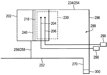
Fig. 10 is a perspective view illustrating an electrical switching device
according to some
inventive principles of this patent disclosure. In this embodiment, the
electrical switching device
200 includes a case 202, contacts 204 and 206, a manual actuator 210, and a
solenoid 212. A
wall 216 within the electrical switching device substantially separates the
contacts 204 and 206
within the case 202 from the manual actuator 210 and the solenoid 212. The
contacts 204 and
206 are coupled to terminals 208 and 209.
12
CA 02709511 2010-07-14
Although the electrical switching device 200 is illustrated apparently as a
cutaway view,
in an embodiment, the electrical switching device 200 can have an open side.
For example, the
case 202 can be configured to include less than all sides to encapsulate the
internal components.
That is, the electrical switching device 200 can be manufactured with the
contacts 204 and 206,
solenoid 212, or the like within the case 202 exposed. In another embodiment,
the electrical
switching device 200 can be configured with a wall enclosing the contacts 204
and 206, solenoid
212, or the like. The electrical switching device 200 can be configured that
such a wall is
removable. For example, the electrical switching device 200 can be an off-the-
shelf component.
In particular, the electrical switching device can be an off the shelf
component substantially
lacking in structures to guide a blast. That is, a blast could exit from the
case 202 of such an off-
the-shelf electrical switching device 200 in an undetermined location on the
case 202. However,
by removing a lid, wall, side, or the like of such an electrical switching
device 200, a blast can be
guided as will be described in further detail below. Regardless, the
electrical switching device
200 includes an opening in the case 202 that is configured to expose the
contacts 204 and 206.
Although an opening in the case 202 has been illustrated as including
substantially all of
one side of the electrical switching device 200, the opening can include more
or less of the case
202. For example, in an embodiment, the case 202 can include an opening that
only exposes the
contacts 204 and 206 within the case. In other words, the manual actuator 210,
the solenoid 212,
or the like within the case 202 may not be exposed through the opening. In
another embodiment,
multiple sides of the electrical switching device 200 can expose the internal
components.
Although a particular type of electrical switching device has been described,
namely an
electrical switching device 200 with a solenoid 212 actuator, any actuator can
be used. In
addition, the electrical switching device 200 can be any switching device as
described above.
Fig. 11 is a cutaway view illustrating a duct according to some inventive
principles of this
patent disclosure. In this embodiment, a case can be arranged to substantially
encapsulate the
electrical switching device 200. A side 234 of the case is illustrated. The
electrical switching
device 200 is disposed in contact with the side.
In the following description, various portions of an electrical switching
device assembly
will be described. However, portions that may have been previously described
or portions that
will be described later may or may not be illustrated. The illustrations may
omit some portions
for the sake of clarity.
13
CA 02709511 2010-07-14
The side 234 includes at least one duct 230. A duct 230 includes one or more
structures
that form an opening. The duct 230 is disposed adjacent to the electrical
switching device 200.
In particular, the duct 230 is disposed adjacent to the opening in the
electrical switching device
200. Accordingly,, as the opening is disposed to expose the contacts 204 and
206 of the electrical
switching device 200, any blast from the contacts 204 and 206 can enter the
duct 230.
In this embodiment, a rib 232 can be disposed in the ducts. The rib 232 can be
disposed
in the duct 230 such that the duct 230 has additional structural support. For
example, the rib 232
can increase a stiffness of the side 234 in the duct 230. In an embodiment,
the duct 230 can be
formed from a recessed region of the side 234. The recessed region can be
strengthened by ribs
232. Although one rib 232 has been described, in an embodiment, multiple ribs
232 can be
disposed in the duct 230 as desired.
In another embodiment, the rib 232 can be configured to contact the case 202
of the
electrical switching device 200. As a result, the rib 232 can provide an
amount of support to the
case 202. Moreover, in an embodiment, the rib 232 can but need not be aligned
substantially
parallel to an axis of the case 202. For example, the rib 232 can be disposed
at an angle, such as
at an angle directed towards a vent. Thus, the rib 232 can be configured to
guide a blast from the
electrical switching device 200.
In another embodiment, the side 234 can include a bulkhead 233. The bulkhead
233 is
disposed extending from a top 235 of the side 234 to the case 202. As
described above, the duct
230 can guide a blast from the electrical switching device 200. However, once
the blast exits the
electrical switching device 200, the blast can expand through any available
opening. The
bulkhead 233 can be configured to substantially isolate other electrical
circuitry from the blast.
That is, the bulkhead 233 can guide -the blast away from travelling around the
case 202.
Fig. 12 is a cross-sectional view illustrating an example of an interface of
the electrical
switching device and case of Fig. 11 along cross-section 231. The case 202 of
the electrical
switching device 200 is in contact with the side 234 of the case. Where the
case 202 contacts the
side 234, the side 234 can include walls 236 and 238. The walls 236 and 238
can be disposed to
contact a perimeter of the case 202. Although walls of the side 234 have been
described, in an
embodiment, the perimeter of the case 202 can contact the surface of the side
234. That is, the
side 234 need not have distinguishable walls to contact the case 202. However,
the case 202 and
the side 234 can still be in contact to aid in guiding a blast.
14
CA 02709511 2010-07-14
Accordingly, the contact of the case 202 and the side 234 forms the duct 230.
Gasses,
particles, or the like from a blast can be exhausted through the duct 230. In
particular, in an
embodiment, the case 202 of the electrical switching device 200 can form an
expansion chamber
coupled to the duct 230. As will be described in further detail below, the
duct 230 can open on
to such an expansion chamber. The blast can be guided into the expansion
chamber where the
gases can expand and cool.
Fig. 13 is an exploded cutaway view of the embodiment of Fig. 11. In this
view, the
electrical switching device 200 is illustrated as offset from the side 234 to
expose the wall 240.
The wall 240 of the side 234 can be disposed within the case 202 of the
electrical switching
device 200.
That is, in an embodiment, the wall 240 can be configured to extend into the
case 202 of
the electrical switching device. The wall 240 can be configured to be disposed
adjacent to the
wall 216 of the case 202. Accordingly, the wall 216 of the case and the wall
240 of the side 234
can function as a bulkhead to contain a blast from the contacts 204 and 206.
Additional walls can also contact the case 202. For example, the walls 236,
238, and 246
of the side 234 and the corresponding perimeter of the case 202 of the
electrical switching device
200 form additional walls. The case 202 can provide additional walls. Such
walls can
substantially contain a blast.
However, because of the interface between the case 202 and the duct 230, an
opening
remains to guide the blast from the chamber 244. As a result, the blast can be
guided away from
the electrical switching device 200.
Fig. 14 is a cross-sectional view illustrating an example of an interface of a
wall of the
case and a wall of the electrical switching device. As described above, a wall
216 can separate
the contacts 204 and 206 from other components of the electrical switching
device 200, such as
the solenoid 212. The wall 240 of the side 234 extends into the electrical
switching device 200.
In this embodiment, the wall 240 partially extends into the electrical
switching device 200.
However, in other embodiments, the wall 240 can fully extend to the opposite
side of the
electrical switching device 200. In another embodiment the wall 240 can form a
butt joint.
That is, the wall 240 of the side 234 and the wall 216 of the electrical
switching device
200 form a wall of a chamber 244. Accordingly, a blast from contacts 204 and
206 can be guided
substantially in a desired direction. Accordingly, any blast from the contacts
204 and 206 can be
CA 02709511 2010-07-14
substantially prevented from traveling towards the solenoid 212 or other
electronics. The blast
can be guided through the duct 230.
In an embodiment, the duct 230 can be the only opening exposing the chamber
244 to a
region external to the electrical switching device 200. For example, the
contact of the walls, the
case 202, and the like can be sealed together. Adhesives, welding, gaskets, or
the like can seal
the surfaces together. As a result, the only route for expanding gas and
particles from the blast is
through the duct 230.
In another embodiment, the duct 230 can be sized such that a majority of the
blast is
directed through the duct 230. For example, there can be some opening between
the wall 216 of
the electrical switching device 200 and the wall 240 of the side 234. Other
interfaces, such as the
interface of the walls 236 and 238 to the perimeter of the electrical
switching device 200 can also
have similar gaps, openings, or the like. As a result, a portion of the blast
can escape beyond the
junction of the walls.
However, the duct 230 can be sized such that a cross-sectional area of an
opening created
in the duct 230 between the side 234 and the electrical switching device 200
can be greater than a
combination of similar cross-sectional areas of the gaps, openings, or the
like described above.
As a result, even though it is possible for the blast to escape through the
other openings, a
majority of the blast can escape through the duct 230.
As illustrated in Fig. 14, the wall 240 can be a planar wall. As illustrated
in Fig. 13, the
wall 240 can include multiple walls. Accordingly, the wall 240 can take any
variety of
configurations. That is, the wall 240 can be disposed on the solenoid 212 side
of the wall 216.
In another embodiment, the wall can straddle the wall 216. In another
embodiment, the wall 240
can be disposed on the contact 206 side of the wall 216.
Fig. 15 is an exploded cutaway view illustrating a bulkhead according to some
inventive
principles of this patent disclosure. Fig. 16 is an exploded cutaway view of
the embodiment of
Fig. 16 from a different angle. Referring to Figs. 15 and 16, in an
embodiment, a first bulkhead
258 can extend between an electrical switching device 200 and a second
bulkhead 252.
In this embodiment, the first bulkhead 258 is part of a center bulkhead 254
dividing the
electrical switching component. When the center bulkhead 254 is assembled with
the side 234,
the bulkhead 258 is disposed between the electrical switching device 200 and
the second
bulkhead 252.
16
CA 02709511 2010-07-14
In an embodiment, the second bulkhead 252 is a circuit board. However, the
second
bulkhead 252 need not be a circuit board. For example, in an embodiment, the
second bulkhead
252 can be a bottom 250 of the electrical switching component, the side 234,
or the like. Thus,
the bulkhead 258 can extend from the electrical switching device 200 to the
bottom 250 of the
electrical switching component. In another embodiment, the second bulkhead 252
can be
another internal structure of the electrical switching component. Similar to
the bulkhead 233
described above, the bulkhead 258 can substantially isolate other electrical
components from the
blast by guiding the blast away from the side of the case 202.
Fig. 17 is a cutaway view illustrating a circuit board in the assembly of Fig.
16 according
to some inventive principles of this patent disclosure. In this view, the
center bulkhead 254 is
assembled with the side 234. The center bulkhead 254 can include a duct 230, a
wall 240, and
the like similar to the side 234. Accordingly, a second electrical switching
device (not
illustrated) similar to the electrical switching device 200 described above
can be assembled with
the center bulkhead. A bulkhead 256 can extend from the electrical switching
device to the
bulkhead 252.
In addition to guiding the blast, the various bulkheads can isolate other
electrical circuitry
from the blast. As described above, a blast can travel through duct 230. The
blast can expand
towards the circuit board 252. The blast can be blocked by the circuit board
252. Accordingly,
electrical components, and in particular, electrical components that are
electrically coupled to
lower voltage circuitry, can be protected from the blast.
Although the bulkhead 256 has been illustrated as substantially in line with
the wall 240,
the bulkhead 256 can be disposed in other locations. For example, the bulkhead
256 can be
disposed further away from the ducts 230. Additional walls such as the wall
242 can contact the
perimeter of the case 202 of the electrical switching device 200. Accordingly,
other components
including the components of the electrical switching device 200 can be
substantially isolated
from the blast.
Although the duct 230 has been illustrated as disposed on the center bulkhead
254, the
duct 230 can be disposed in other locations. In an embodiment, the duct 230
can be disposed on
another side (not illustrated) of the electrical switching component opposite
the side 234. In
another embodiment, the ducts for multiple electrical switching devices 200
can be disposed on
17
CA 02709511 2010-07-14
the center bulkhead 254. The openings of the electrical switching devices 200
can be disposed to
open on to the duct 230, regardless of the particular location.
Fig. 18 is a cutaway view illustrating a circuit board according to some
inventive
principles of this patent disclosure. In this embodiment, the circuit board
252 is mounted to the
side 234 and the bottom 250. The circuit board 252 can be similarly mounted on
another side of
the case (not illustrated). The circuit board 252 is supported by stand-offs
270 and 272. The
stand-offs 270 and 272 can be configured to offset the circuit board 252 from
the bottom 250.
As a result, circuitry can be disposed on side 255 of the circuit board 252.
In addition to supporting the circuit board 252, the stand-off 270 can
substantially isolate
the opposite side 255 of the circuit board 252. For example, the blast can be
directed along the
circuit board 252. The stand-off 270 can also be configured to direct such a
blast away from the
opposite side 255 of the circuit board 252.
Fig. 19 is the cutaway view of Fig. 18 without the circuit board. Supports 280
and 282
can be configured to support an edge of the circuit board 252. For example,
the circuit board 252
can be disposed between the supports 280 and 282.
The supports 280 and 282 can extend along a length of the circuit board 252.
In
particular, in an embodiment, the support 280 can extend along a length of the
circuit board 252.
Accordingly, when a blast increases the pressure on the circuit board 252, the
circuit board 252
can be pressed on to the support 280. Thus, the blast can be substantially
prevented from
escaping around an edge of the circuit board extending along the length.
The support 280 can, but need not extend along the entire length of the
circuit board 252.
For example, the support can extend only along a length of the circuit board
252 where the
circuit board 252 may encounter a blast. Similarly, the support 282 can, but
need not extend
along an entire length of the circuit board 252. For example, the support 282
can include
periodically spaced supports along the edge. Although the support 280 has been
illustrated as
continuous along a length of the circuit board 252, the support 280 can
include periodically
spaced structures.
The supports 280 and 282 have been illustrated for an example. Other supports
can be
included on another side of the case, a center bulkhead 254, or the like.
Accordingly, along a
perimeter of the circuit board 252, the edges of the circuit board 252 can be
substantially sealed.
However, in an embodiment, the edges of the circuit board can, but need not be
substantially
18
CA 02709511 2010-07-14
sealed beyond a bulkhead, such as bulkhead 256 or 258. That is, if the blast
is substantially
isolated from a region of the circuit board 252, the edges in that region need
not be substantially
sealed.
Moreover, although the supports'280 and 282 have been illustrated as
protrusions, the
supports 280 and 282 can take different forms. For example, the supports 280
and 282 can
include a slot, recessed region of the side 234, or the like configured to
receive an edge of the
circuit board 252. Any combination of such protrusions and recessed regions
can be used.
Fig. 20 is a cutaway view illustrating a bulkhead and terminals according to
some
inventive principles of this patent disclosure. In this embodiment, a second
electrical switching
device 200 is illustrated as assembled on the center bulkhead 254. The
contacts of the electrical
switching device 200 are coupled to conductors 294. The conductors 294 are
coupled to
corresponding terminals 290. The terminals 290 can be configured to be coupled
to wiring 292.
Although the terminals 290 have been illustrated as screw terminals, the
terminals 290
can have a variety of configurations. For example, the terminals 290 can be
quick connect
terminals, connectors, or the like.
A blast from the electrical switching device 200 can travel through the
chamber including
the conductors 294. However, a bulkhead 296 can be disposed between the
electrical switching
device 200 and the terminals 290. The conductors 294 can be disposed to extend
through the
bulkhead where the bulkhead 296 can be configured to substantially isolate the
terminals 290
from a blast.
As illustrated in FIG. 20, the bulkhead 296 is part of the center bulkhead
254. However,
a gap 295 can be present in the bulkhead 296 to allow for placement of the
conductors 294. The
gap 295 can be substantially filled by a corresponding structure on another
side (not illustrated)
of the electrical switching component. Accordingly, although the bulkhead 296
has been
described as substantially isolating the terminals 290 from a blast, the
isolation can include a
contribution from the additional structure of the other side. Moreover,
although the bulkhead
296 has been illustrated as an internal bulkhead, the bulkhead 296 can be
formed from a side of
the case, such as side 234. That is, in an embodiment, the bulkhead 296 can be
a wall of the
case.
Fig. 21 is the cutaway view of Fig. 20 rotated to illustrate a vent according
to some
inventive principles of this patent disclosure. As described above, a vent 300
can be disposed in
19
CA 02709511 2010-07-14
the case to allow a blast to vent to outside of the case. In this embodiment,
the vent 300 is
disposed between the electrical switching device 200 and the bulkhead 296.
However, in other
embodiments, the vent 300 can be disposed anywhere such that there is a
substantially
continuous path between, the electrical switching device 200 and the vent.
Accordingly, a blast can occur in the electrical switching device 200. The
blast can be
guided through the ducts 230. The ducts 230 can vent into the chamber defined
by the center
bulkhead 254, the circuit board 252, the bulkhead 256, the bulkhead 296, and
the other side (not
illustrated). As the chamber is larger than the chamber 244 of the electrical
switching device
200, the blast can expand, reducing the temperature and pressure. The gap
between the stand-off
270 and the bulkhead 296 directs the blast towards the vent 300 and towards an
exterior of the
electrical switching component.
Similar to the size of the duct relative to the size of any opening created by
the junction
of the case 202 of the electrical switching device 200 and the side 234, the
size of the vent 300
can be selected such that a cross-sectional opening of the vent 300 is larger
than a combination
of other gaps, openings, or the like between the various sides, circuit board,
bulkheads, and the
like guiding the blast. Accordingly, a substantial amount of the blast can be
guided out of the
vent 300.
In an embodiment, the electrical switching component can include multiple
bulkheads
disposed between the electrical switching device 200 and the terminals 290. As
illustrated in
Fig. 21, the conductor 294 extends through bulkhead 297. In this embodiment,
only one of the
conductors 294 passes through a bulkhead 297 in addition to the bulkhead 296.
However, in
other embodiments, the other conductor 294, each of the conductors 294, or the
like can pass
through multiple bulkheads between the electrical switching device 200 and the
terminals 290.
In an embodiment, the conductor 294 that is furthest from the vent 300 can
pass through
bulkhead 297. A blast guided by the ducts 230 and directed towards the
bulkhead 297 may not
have fully expanded and could have a pressure high enough to blow past an
interface of the
conductor 294 and the bulkhead 296. However, the bulkhead 297 can redirect the
blast such that
the blast can further expand, reduce in pressure, temperature, or the like,
before the blast reaches
an interface exposing the outside of the electrical switching component. That
is, the shock front
of the blast can be guided such that pressure is reduced before the blast has
an opportunity to
escape the electrical switching component.
CA 02709511 2010-07-14
Moreover, in an embodiment, the bulkhead 297 can create a substantially
separate
chamber 299. The chamber 299 can be formed from a curvature of the bulkhead
297 towards the
bulkhead 296. Other structures such as the center bulkhead 254 or the like can
create other sides
of the chamber 299. Accordingly, a blast must travel through multiple
chambers, experiencing
an expansion out of the duct 230, a constriction when passing through a gap
287, another
expansion in chamber 299, and so on. Multiple chambers such as chamber 299 can
be created
such that a blast travelling towards the terminal 209 can experience such
expansions and
constrictions. As a result, the interfaces of the sides, bulkheads, walls, or
the like can be more
likely to contain the blast and guide it to the intended vent 300.
Fig. 22 is a cross-sectional view illustrating a second chamber according to
some
inventive principles of this patent disclosure. Fig. 23 is a cross-sectional
view along plane 298
illustrating a wall of the second chamber of Fig. 22 according to some
inventive principles of this
patent disclosure. In the embodiment of Fig. 21, the bulkheads 299 and 296 are
illustrated as
including gaps 287 and 295 allowing the conductor 294 to be assembled in the
electrical
switching component. In contrast, in the embodiment of Fig. 22, the
corresponding gaps are on
opposite sides of the conductor 294.
For example, the center bulkhead 254 includes the bulkhead 296. The bulkhead
296
extends towards the side 234. As described above, a gap 295 is present to
allow assembly. A tab
291, illustrated in phantom, can substantially fill the gap 295, substantially
sealing that wall of
the chamber 299. In contrast, the gap 287 of the bulkhead 297 is disposed on
an opposite side of
the conductor 294. Moreover, the bulkhead 297 is disposed on the side 234, not
on the center
bulkhead 254 as illustrated in Fig. 21. A tab 291 of the center bulkhead 254
extends to fill the
gap 297 of the bulkhead 297.
The cross-sectional view along plane 289 is illustrated for bulkhead 297.
However, the
orientation of the gap 295 and the bulkhead 296 are on opposite sides for a
similar cross-section.
A blast can escape through the gaps in such structures. However, a blast
travelling along
conductor 294 will not have a substantially straight path through chamber 299.
That is, because
of the orientation of the gaps, the blast can change direction, deposit
suspended particles on the
walls, and further isolate the terminal 290 and any wiring from the blast.
Fig. 24 is a block diagram illustrating an example of guiding a blast
according to some
inventive principles of this patent disclosure. In this embodiment various
components described
21
CA 02709511 2010-07-14
above are conceptually illustrated to show a path traveled by a blast. A case
202 of an electrical
switching device 200 includes the contacts 204 and 206 where a blast occurs.
Walls 216 and 240
contain the blast and, with the case 202, guide the blast through the ducts
230 into an expansion
chamber 298.
The chamber 298 is bounded by the center bulkhead 254, a corresponding side
such as
side 234, bulkhead 296, bulkhead 256 or 258, circuit board 252, and stand-off
270. In one
example, a blast can be deflected by the center bulkhead 254 or side 234,
directed towards the
vent 300 by bulkhead 298. In another example, the blast can be deflected by
walls 256 or 258,
and circuit board 252 towards the vent 300. Accordingly, in an embodiment,
each of the various
walls, bulkheads, circuit boards, and the like contribute to containing the
blast and guiding it
towards the vent 300.
Moreover, in an embodiment, the electrical switching component can form a
module.
That is, the electrical switching device 200, which has its own case 202, can
be encapsulated
within the case formed by the various walls, bulkheads, and the like described
above to form a
modular component.
Fig. 25 is a block diagram illustrating various zones according to some
inventive
principles of this patent disclosure. As described above, walls 256 and 258,
and stand-off 270
can substantially isolate portions of the circuit board 252 from a blast. Fig.
25 illustrates a top
view of the circuit board 252. Walls 256 and 258 can divide the circuit board
252 into two
different zones 301 and 302.
Zone 301 can be a high voltage circuit zone. That is, high voltage circuitry,
relays,
switches, or the like can be disposed in circuit zone 301. For example,
various components that
may be coupled to the electrical switching device 200, the conductors 294, or
the like within the
electrical switching component can be coupled to the circuit board 252 in zone
301. In addition,
circuit zone 301 can include the portion of the circuit board 252 that can
deflect a blast as
described above. Accordingly, as a blast can create short circuits between a
line terminal of the
electrical switching component, circuitry within the zone 301 could be
subjected such line
voltages. Accordingly, the circuitry in zone 301 could be exposed to a voltage
range including
high voltages.
In contrast, circuit zone 302 can be substantially isolated from the blast. As
described
above, the walls 256 and/or 258 can prevent an amount of the blast from
reaching circuitry
22
CA 02709511 2010-07-14
within zone 302. Accordingly, the circuitry in zone 302 can be exposed to a
voltage range
including maximum voltages lower than that of circuit zone 301. That is, even
after a blast, short
circuits caused by the blast may not cause high voltages to be conducted to
circuitry in zone 302.
Thus, low voltage circuitry, processors, interfaces, or the like can be placed
in zone 302.
Fig. 26 is a block diagram illustrating additional zones of the circuit board
of Fig. 25
according to some inventive principles of this patent disclosure. Fig. 24
illustrates the opposite
side of circuit board 252. Walls 256 and 258 are illustrated in phantom for
reference.
This side of the circuit board 252 includes zones 305 and 306. The zones 305
and 306
can be divided by an isolator 303. The isolator 303 can form a division 307
between the zones
305 and 306. The isolator 303 can be a variety of devices. For example, the
isolator 303 can be
an opto-isolator, a transformer, or the like such that current is
substantially prevented from
flowing directly across the isolator 303.
In zone 305, circuitry can be present that does not operate in the high
voltage range of
zone 301. However, zone 305 can include through-hole components that penetrate
the circuit
board 252. As a result, the components can have electrical contact with zone
301 on the opposite
side. As a result, in the event of a blast, a short circuit in zone 301 can
cause a high voltage to
appear on circuitry in zone 305.
Accordingly, at least one isolator 303 can allow signals to pass between zones
305 and
306. Any high voltage in zone 305 can be contained in zone 305. Note that as
the blast can be
substantially isolated from this side of the circuit board 252, materials that
can create short
circuits will likely not be deposited in either zones 305 or 306. As a result,
a short will likely not
be created across the isolator 303. Thus, the isolator 303 can bridge the
division 307 of zones
305 and 306.
Fig. 27 is a perspective view illustrating an electrical switching component
according to
some inventive principles of this patent disclosure. In this embodiment, an
electrical switching
.component 310 can include a case 311 and a connector 316. An additional
connector 318 is
illustrated; however, any number of connectors can be used.
The connector 316 is disposed on a first end of the case such that the
connector 316 can
be coupled to a second connector (not illustrated) on a mounting site 324 by
moving the case 311
in a direction 320. That is the connector 316 is disposed on the case 311 such
that movement on
direction 320 can engage the connector 316.
23
CA 02709511 2010-07-14
The case 311 includes a retaining structure 312. The retaining structure 312
is configured
to be constrained such that movement of the case in the direction 320 is
limited. For example, a
panel 322 of an enclosure containing the electrical switching component 310
can be installed
after the electrical switching component 310 is mounted on the mounting site
324. As a result,
the movement of the electrical switching component 310 is constrained along
direction 320.
That is, the mounting site 324 can prevent the electrical switching component
310 from moving
in the direction of the arrow of direction 320 while the plate 322 can be
configured to prevent the
electrical switching component 310 from moving in a direction opposite the
arrow of direction
320.
As illustrated, the retaining structure 312 can include a protrusion extending
from a
surface of the case 311. The plate 322 can be disposed on a side of the
retaining structure 312
opposite the mounting site 324.
In another embodiment, the retaining structure 312 can include a recessed
region within a
surface of the case 311. The recessed region can be configured to receive a
corresponding tab,
protrusion, or other structure of the plate 322.
In another embodiment, the retaining structure 312 can include mounting
locations for a
fastener. For example, a fastener can include a screw, brad, bolt, nut, or the
like. The case 311
can include a threaded hole configured to receive a screw, for example.
Accordingly, the plate
322 can be mounted to the case 311 using the retaining structure 312.
In an embodiment, the electrical switching component 310 can include a manual
actuator
314 coupled to an electrical switching device of the electrical switching
component 310 as
described above. The manual actuator 314 can be configured to change a state
of the electrical
switching device as the manual actuator is actuated in the direction 320.
Since the manual actuator 314 can be actuated in the direction 320, the force
applied to
actuate the manual actuator 314 has the potential to dislodge the electrical
switching component
310 from the mounting site 324. However, since.the retaining structure 312 is
coupled with the
plate 322, limiting the movement along direction 320, such actuation of the
manual actuator 314
can reduce a chance that the force applied will dislodge the electrical
switching component 310.
Fig. 28 is a cutaway view illustrating an actuator according to some inventive
principles
of this patent disclosure. The manual. actuator 314 can include an end 334.
The end 334 can be
configured to actuate a photointerruptor 332. The photointerruptor 332 can be
disposed on the
24
CA 02709511 2010-07-14
circuit board 252 described above. Accordingly, when the manual actuator 314
is actuated, such
actuation can be sensed. In addition, the manual actuator 314 can be
configured to move when
the electrical switching device 200 is electrically actuated. That is, when
the electrical switching
device 200 is actuated by an electronic signal, the electrical switching
device 200 can cause the
manual actuator 314 to be actuated. Such actuation can also be sensed by the
photointerruptor
332 and interpreted as the position of the manual actuator 314 and hence, the
state of the
electrical switching device 200. That is, from the position, a state of the
electrical switching
device can be sensed. For example, not only can an on/off state be sensed, but
with an
appropriately configured sensor, other states, such as a tripped state can be
sensed.
In an embodiment, the manual actuator 314 need not be present, yet the
actuation of the
electrical switching device 200 can still be sensed. For example, the manual
actuator 314 can be
replaced with a linkage configured to couple contacts or other structures of
the electrical
switching device 200 to the photointerruptor 332. Thus, the actuation can be
sensed without a
manual actuator 314. However, in another embodiment, such linkages can include
the manual
actuator 314.
Although a photointerruptor has been described above, other types of sensors
can be
used. For example, a mechanical contact sensor that makes or breaks an
electrical circuit can be
used. A digital position encoder can be used to sense the position of the end
334. Any sensor
that can sense position, movement, acceleration, or the like can be used.
As described above, the electrical switching component 310 can have both high
voltage
circuitry and low voltage circuitry. In an embodiment the high voltage
circuitry can be
substantially isolated from a user. That is, a user may be required to remove
panels, cases,
enclosures, or the like beyond that used in normal operations to access the
high voltage circuitry.
Accordingly, the retaining structure 312 can be disposed on the case 311 to
facilitate such
isolation from a user. For example, as described above, the assembly can have
various high
voltage circuitry, conductors, or the like. Line 336 conceptually divides the
electrical switching
component 310 into high voltage and low voltage regions. At one end of the
electrical switching
component 310 with the terminals 290, high voltage circuitry is exposed
through an opening of
the case 311. At another end of the electrical switching component 310 with
the connectors 316
and 318, low voltage circuitry is exposed through the case 311.
CA 02709511 2010-07-14
The retaining structure 312 can be disposed on the case 311 between such
openings.
Accordingly, when secured by the panel 322 described above or other similar
structure, the high
voltage electrical circuitry and, in particular, the exposed contacts such as
the terminals 290 of
the high voltage circuitry can be substantially isolated from a user.
Fig. 29 is a perspective view illustrating a case according to some inventive
principles of
this patent disclosure. In this embodiment, the case 311 of the electrical
switching component
310 includes a protrusion 340 extending from a surface of the case 311. The
protrusion 340 can
extend from a side of the case opposite the retaining structure 312.
The protrusion 340 can be aligned along the direction such that when the
protrusion is
disposed in a corresponding opening, the case is substantially constrained in
a second direction
344 substantially orthogonal to the first direction 320. The protrusion 340
can be aligned such
that the case 311 is not substantially constrained when disposed in the
corresponding opening in
direction 320.
For example, the opening can be a slot aligned with a long axis in direction
320. The
protrusion 340 can have a width in direction 344 substantially equal to the
width of the slot,
while a length of the protrusion 340 is less than a corresponding length of
the slot in direction
320. Thus, the electrical switching component 310 can have a range of motion
along direction
320 while being substantially constrained in direction 344.
In an embodiment, the case 311 can include a second protrusion 342. The second
protrusion can be disposed on the same side of the case 311 as the first
protrusion 340 opposite
the retaining structure 312. The second protrusion 342 can, but need not be
shaped similarly to
the first protrusion. The second protrusion 342 can be similarly formed to
constrain the motion
of the electrical switching component 310 when disposed in a corresponding
opening as is the
first protrusion 340.
The first protrusion 340 and the second protrusion 342 can be disposed on
opposite edges
of case 311. For example, the first protrusion 340 can be disposed on a first
edge 341 of the case
311. The second protrusion 342 can be disposed on a second edge 343. Although
the edges 341
and 343 can be on the same side of the case 311 opposite the retaining
structure 312, the edges
341 and 343 can be on opposite edges of that side.
In an embodiment, the protrusions 340 and 342 can be offset from each other
along
direction 320. That is, along the direction of insertion for mounting the
electrical switching
26
CA 02709511 2010-07-14
component 310, the protrusions 340 and 342 can be offset. However, in other
embodiments, the
protrusions 340 and 342 need not be offset.
In an embodiment, mounting ears 346 can be disposed on the case 311 to mount
the
electrical switching component 310 to a mounting location. For example, the
mounting location
can have an opening configured to receive the mounting ears 346.
Fig. 30 is a side view illustrating the protrusion and mounting ear of Fig.
29. The
protrusion 340 can have a height 348 that is greater than a height 350 of the
mounting ear 346.
Accordingly, in an embodiment, when being mounted on a mounting site, the
protrusion 340 can
contact the mounting site prior to the mounting ear 346. As a result, when the
protrusion 340 is
aligned with a corresponding opening, the protrusion 340 can pass through the
opening, allowing
the mounting ear 346 to approach the mounting site.
Fig. 31 is a plan view of an example of a mounting site for the assembly of
Fig. 29. In
this embodiment, the side of the case 311 opposite the retaining structure 312
is illustrated in
phantom. Fig. 31 illustrates a state where the electrical switching component
310 is mounted on
the mounting site 380, but the mounting ears 346 are not engaged. The mounting
site 380
includes openings 370, 372, and 374. The protrusions 340 and 342 are disposed
in openings 370
and 372, respectively. The mounting ears 346 are disposed in the openings 374.
As described above, the protrusions 370 and 372 can be higher than the
mounting ears
346. Accordingly, when the electrical switching component 310 is brought into
contact with the
.20 mounting site 380, the contact will be with the protrusions 340 and 342.
In an embodiment, the openings 370 and 372 can be longer along direction 320
than
necessary to accommodate a range of motion of the electrical switching
component 310 when the
mounting ears 346 are disposed in the openings 376. That is, a greater amount
of misalignment
of the protrusions 340 and 342 relative to an installed location can be
tolerated with the openings
370 and 372.
Accordingly, the protrusions 340 and 342 can engage with the openings 370 and
372 with
an amount of misalignment between the mounting ears 346 and the openings 376.
However, this
does not mean that the mounting ears 346 cannot engage the openings as the
protrusions 340 and
342 can engage with the openings 370 and 372. If the protrusions 340 and 342
engage with the
openings 370 and 372 with the mounting ears 346 misaligned, the mounting ears
346 can contact
the mounting site 380 and slide along as the electrical switching component
310 is moved.
27
CA 02709511 2010-07-14
As the protrusions 340 and 342 are engaged with the openings 370 and 372, the
motion
of the electrical switching component 310 is constrained. Thus, the motion of
the assembly, is
limited in direction 344; however, the motion in direction 320 is possible due
to the relative
lengths of the protrusions 340 and 372 and the openings 370 and 372. The
electrical switching
component 310 can be moved along direction 320 until the mounting ears 346
pass through the
openings 374. The electrical switching device 310 can then be moved again
along direction 320
to engage the mounting ears 346 with the mounting site 380.
Although the mounting ears 346 have been used as an example, other mounting
structures
can be used. For example, clips, hooks, or the like can be used to mount the
electrical switching
device 310 to the mounting site 380.
The inventive principles of this patent disclosure have been described above
with
reference to some specific example embodiments, but these embodiments can be
modified in
arrangement and detail without departing from the inventive concepts. For
example, in some
embodiments, a circuit board may be part of the electrical switching
component, while in other
embodiments, a circuit board may be all or part of a chassis to which the
component is mounted.
As another example, the switching device need not be a simple on-off device,
but may provide
continuous control such as that provided by an SCR, triac, transistor, etc.
Such changes and
modifications are considered to fall within the scope of the following claims.
28