Note: Descriptions are shown in the official language in which they were submitted.
CA 02709616 2010-07-13
-1-
MULTI-SLOT ANTENNA AND MOBILE DEVICE
FIELD
[0001] The present application generally relates to an antenna and, in
particular, to a multi-slot antenna and a mobile device incorporating the
multi-
slot antenna.
BACKGROUND
[0002] Modern mobile communications devices are often equipped to
operate on more than one frequency band. For example, some devices are
capable of communicating on GSM-850 and GSM-1900. Yet other devices are
capable of communication on GSM-900 and GSM-1800. Some tri-band devices,
or even quad-band devices are configured to operate on three or four bands.
[0003] In addition, modern mobile communications devices are often multi-
mode devices configured to communicate in more than one mode. For example,
a multi-mode device may be configured to communicate with WWAN (wireless
wide area networks) in accordance with standards such as GSM, EDGE, 3GPP,
UMTS, etc., and may further be configured to communicate with WLAN (wireless
local area networks) in accordance with standards like IEEE 802.11. Some
devices are also equipped for short-range communications such as BluetoothTM
The multi-functionality of these devices often requires multiple antennas
within
the devices in order to communicate over the various frequency bands.
[0004] At the same time, the form factors for mobile communications
devices are increasingly sleek and compact. This puts space within the device
at
a premium and makes it difficult to accommodate multiple antennas.
[0005] It would be advantageous to provide for an antenna that has a low
profile but is capable of operating on multiple frequency bands.
R&M 42783-2063 RIM 36098-CA-PAT
CA 02709616 2010-07-13
-2-
BRIEF SUMMARY
[0006] In one aspect, the present application describes a mobile
communication device. The device includes a dielectric substrate having a
surface; a radio frequency patch antenna formed from a conductive material on
the surface of the substrate; a signal feed conductor connected to the patch
antenna; and a ground conductor connecting the patch antenna to a ground
plane. The patch antenna has defined therein at least two slots.
[0007] In another aspect, the present application describes a mobile
communication device. The device includes a dielectric substrate having a
surface; a radio frequency multi-band patch antenna formed from a conductive
material on the surface of the substrate; a signal feed conductor connected to
the patch antenna; and a ground conductor connecting the patch antenna to a
ground plane. The patch antenna has defined therein a first slot and a second
slot. The first slot and the second slot each have two or more parts.
[0008] In yet another aspect, the present application describes a multiband
antenna that includes a dielectric substrate having a surface; a patch of
conductive material on the surface of the substrate; a signal feed conductor
connected to the patch; and a ground conductor connecting to the patch. The
patch has defined therein at least two slots. The at least two slots each have
two
or more parts.
[0009] In some cases at least one part of each of the first and second slots
is open to an edge of the patch. In some embodiments, the second slot is
disposed on the patch between at least one of the parts of the first slot and
the
edge of the patch. In some embodiments, the signal feed conductor is
connected to the patch between the first and second slots. In some
embodiments, the signal feed conductor is connected to the edge of the patch
between the parts of the respective first and second slot that are open to
that
edge.
[0010] In some embodiments, the first and second slots include an L-
shaped slot and a C-shaped slot. In some embodiments, the L-shaped slot is an
R&M 42783-2063 RIM 36098-CA-PAT
CA 02709616 2010-07-13
-3-
open slot projecting into the patch antenna from an edge. In some
embodiments, the C-shaped slot is also an open slot projecting into the patch
antenna from the edge. The signal feed conductor may be connected to the
same edge of the patch antenna at a point between the L-shaped slot and the C-
shaped slot. In some embodiments, the C-shaped slot is nested within the L-
shaped slot.
BRIEF DESCRIPTION OF THE DRAWINGS
[0011] Reference will now be made, by way of example, to the
accompanying drawings which show example embodiments of the present
application, and in which:
[0012] Figure 1 diagrammatically shows an embodiment of an antenna;
[0013] Figure 2 shows a dimensioned illustration of an embodiment of the
antenna;
[0014] Figure 3 shows a side view of one embodiment of the antenna;
[0015] Figure 4 shows a bottom perspective view of the antenna of Figure
3;
[0016] Figure 5 shows a top perspective view of another embodiment of an
antenna;
[0017] Figure 6 shows a front perspective view of the antenna of Figure 5;
[0018] Figure 7 shows a bottom perspective view of the antenna of Figure
5;
[0019] Figure 8 shows a portion of a mobile device incorporating the
antenna of Figure 5;
[0020] Figure 9 shows an S11 plot for the antenna of Figure 6;
[0021] Figure 10 shows a perspective view of another embodiment of an
antenna; and
R&M 42783-2063 RIM 36098-CA-PAT
CA 02709616 2010-07-13
-4-
[0022] Figure 11 shows a block diagram of a handheld electronic device
incorporating the antenna.
[0023] Similar reference numerals may have been used in different figures
to denote similar components.
DESCRIPTION OF EXAMPLE EMBODIMENTS
[0024] Many electronic devices include an antenna for radio frequency
communications, including mobile devices, laptop computers, desktop
computers, smartphones, personal digital assistants, and many other such
devices. Multi-mode or multi-band devices are configured to operate on more
than one frequency band. Accordingly, such devices required more than one
antenna or at least one antenna that is capable of operating on more than one
band.
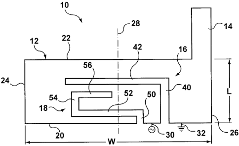
[0025] Reference is now made to Figure 1, which diagrammatically
illustrates an example embodiment of an antenna 10. The antenna 10 is a low
profile patch antenna formed from a conducting material, such as a metal. In
this embodiment, the patch antenna 10 includes a main patch, formed as a
generally rectangular portion 12 having a length L and width W. The generally
rectangular portion 12 includes a lower edge 20, and upper edge 22, a left
edge
24 and a right edge 26. In other embodiments, other shapes for the patch
antenna may be used, including other polygonal shapes.
[0026] In this embodiment, a tuning stub 14 extends from one side of the
rectangular portion 12. In this embodiment, the tuning stub 14 extends from
the
right side of the upper edge 22. The tuning stub 14 is integral with the
rectangular portion 12 to form a single polygonal patch. The tuning stub 14 is
placed and sized to tune the common mode resonance of the antenna 10, as will
be described further below. Those ordinarily skilled in the art will
appreciate that
the patch antenna 10 need not necessarily include the tuning stub 14 and that
the dimensions and shape of the patch may be adjusted to tune the common
mode resonance of the antenna 10. Industrial design restrictions imposed by
the
R&M 42783-2063 RIM 36098-CA-PAT
CA 02709616 2010-07-13
-5-
form factor of the mobile device or other device in which the antenna 10 will
be
used may make use of the tuning stub 14 advantageous for those situations in
which particular dimensions of the patch cannot be varied in a manner to
achieve
the desired resonance.
[0027] A signal feed conductor 30 connects to the lower edge 20 of the
rectangular portion 12. The signal feed conductor 30 supply excitation current
to
the antenna 10 from driving circuitry, such as a transceiver (not shown). When
used for reception, the signal feed conductor 30 conducts current induced in
the
antenna 10 by incident RF signals to receiving circuitry (not shown), such as
a
transceiver for filtering, amplification and demodulation. The signal feed
conductor 30 in this embodiment connects to the lower edge 20 at a position to
the right of the center of the rectangular portion 12. The centerline of the
rectangular portion 12 is illustrated by a dashed line labeled 28. Although in
the
embodiments described herein the signal feed conductor 30 may be considered a
microstrip-type direct feed connector, those ordinarily skilled in the art
will
appreciate that the signal feed conductor may be a different type of feed. For
example, in some embodiments, a coax feed connector may be used. In yet
other embodiments, an indirect coupling may be used, such as a capacitive or
inductive coupling.
[0028] A ground conductor 32 also connects to the lower edge 20 of the
rectangular portion 12. The ground conductor 32 connects to a ground plane
(not shown). The ground plane is typically roughly parallel to and spaced
apart
from the antenna 10. In an electronic device, the antenna 10 may be supported
by or mounted upon a non-conducting substrate of suitable dielectric material.
The dielectric material may space the antenna 10 apart from an underlying
ground plane in some embodiments.
[0029] Two or more slots (individually labeled 16 and 18) are formed in the
generally rectangular portion 12. The two or more slots 16 and 18 each have
two or more parts. The term "parts" in this context refers to the joined
segments that make up the slot. In the embodiment shown the segments are
straight-line segments or parts that are joined at right-angles; however, it
will be
R&M 42783-2063 RIM 36098-CA-PAT
CA 02709616 2010-07-13
-6-
understood that in some embodiments one or more parts may not be straight,
and two parts may be joined at an angle other than a right angle. In some
cases,
a part may be curved or have a non-uniform width. In this embodiment, the
slots are an L-shaped slot 16 and a C-shaped slot 18, and they extend from the
lower edge 20 of the generally rectangular portion 12.
[0030] The slots 16 and 18 in this embodiment are of different length.
Accordingly, they have different resonant frequencies; however, in this
embodiment they are formed to have resonant frequencies sufficiently close
that
in combination they result in wideband performance for the antenna 10.
[0031] In this particular embodiment, the slots 16 and 18 are located on
either side of the signal feed conductor 30. In particular, the L-shaped slot
16
extends from the lower edge 20 to the right of the signal feed conductor 30
and
the C-shaped slot extends from the lower edge 20 to the left of the signal
feed
conductor 30. The L-shaped slot 16 has a first section 40 that extends upwards
from the lower edge 20 in the direction of the upper edge 22, and a second
section 42 that extends from the upper end of the first section 42
perpendicular
to the first section 40 towards the left edge 24. The second section 42 in
this
embodiment extends beyond the centerline 28.
[0032] In this embodiment, the C-shaped slot 18 is an open C-shape facing
towards the L-shaped slot 16. In particular, the C-shaped slot 18 includes a
first
portion 50 that extends perpendicularly from the lower edge 20 towards the
upper edge 22. It then includes a second portion 52 that extends perpendicular
to the first portion 50 towards the left edge 24. The second portion 52
extends
beyond the centerline 28. The C-shaped slot 18 then includes a third portion
54
and a fourth portion 56 to form the C-shape.
[0033] In this embodiment, the C-shaped slot 18 is at least partly nested
below or in the L-shaped slot 16. In particular, the C-shaped slot 18 is
disposed
between the second section 42 of the L-shaped slot 16 and the edge 20.
R&M 42783-2063 RIM 36098-CA-PAT
CA 02709616 2010-07-13
-7-
[0034] The length and relative positioning of the C-shaped slot 18 and L-
shaped slot 16 produce two slot-based resonances that create a coupling effect
that improves the impedance matching for the desired frequency bands to
produce a wideband resonance for the antenna 10.
[0035] Because the slots 16, 18 are open at the edge 20, they are termed
"open" slots, as opposed to "closed" slots. A "closed" slot is one located
entirely
within the boundaries or edges of the patch. In some embodiments, the C-
shaped slot 18 may be a closed slot. The L-shaped slot 16 may, in some
embodiments be a closed slot; however, in its location shown in Figure 1 it
serves to separate the current paths of the signal feed conductor 30 from the
ground conductor 32. Accordingly, if the L-shaped slot 16 were made a closed
slot, the signal feed conductor 30 or the ground conductor 32 may need to be
relocated to another areas of the antenna 10. Such relocation, would, of
course,
alter the current paths and resulting resonances.
[0036] It will be appreciated that in other embodiments, different shaped
slots may be used to realize different current paths, and that different
shaped
slots may result in positive or negative coupling of the respective resonances
depending on their relative shapes and distances apart in terms of fractions
of
resonant wavelengths. The slots may be lengthened or shortened to tune the
resonances to particular desired frequencies. Additional slots may be added to
create additional resonances to support additional bands of operation, or to
tune
or increase the bandwidth of the wideband response. It will also be
appreciated
that additional elements, including parasitic patches may be added to further
tune or shape the performance of the antenna 10.
[0037] The multi-band antenna 10 shown in Figure 1 includes three
resonances. The first resonance is a common mode resonance set by the
dimensions of the generally rectangular portion 12 and the location of the
signal
feed conductor 30, and tuned by the tuning stub 14. The second and third
resonances are slot resonances determined by the dimensions of the slots 16,
18. As noted above, if the dimensions are such that the resonances are
R&M 42783-2063 RIM 36098-CA-PAT
CA 02709616 2010-07-13
-8-
somewhat close together in frequency, they merge to enable wideband
communications.
[0038] In the embodiment illustrated in Figure 1, the shape and
configuration of the slots 16, 18 contributes to obtaining a positive coupling
between the two slot resonances that improves the wideband performance of the
antenna 10. In some other embodiments, the slots may be arranged such that
they do not result in positive coupling and have more distinctive resonances.
[0039] The generally rectangular portion 12 has the left edge 24 and right
edge 26 that respectively define a left portion and right portion on either
side of
the slots 16 and 18. The sizes of these portions or regions may be adjusted to
tune the antenna 10. In particular, increasing or decreasing the size of the
left
portion or region may tune the common mode resonance. Increasing or
decreasing the size of the right portion or region may tune the common mode
resonance and the slot resonances.
[0040] Reference is now made to Figure 2, which shows the example
antenna 10 with sample dimensions. In particular, the dimensions of the slots
16, 18 for a particular embodiment are illustrated. The L-shaped slot 16 has a
first section 40 that extends upwards 10.3 mm, and a second section 42 that is
29.8 mm long. The first section 40 is 1.65 mm wide and the second section 42
is 1.18 mm wide.
[0041] The C-shaped slot 18 has a first portion 1.1 mm wide and 2.8 mm
long, a second portion 1.0 mm wide and 21.35 mm long, a third portion 1.25
mm wide and 5.3 mm long, and a fourth portion 1.1 mm wide and 10.8 mm
long. As noted previously, adjustments to the dimensions will impact the
impedance and resonance of the slots 16, 18.
[0042] The "sections" or "portions" of the slots may also be referred to
herein as "parts" of the slots.
R&M 42783-2063 RIM 36098-CA-PAT
CA 02709616 2010-07-13
-9-
[0043] The first portion of the C-shaped slot 18 is separated from the first
section of the L-shaped slot 16 by 5.3 mm.
[0044] The tuning stub, in this embodiment, is 18.3 mm long and 3.7 mm
wide. The rectangular portion is approximately 14 mm from its upper edge to
its
lower edge.
[0045] The dimensions for the slots given above and in connection with
Figure 2 have been selected to realize slot resonances in the range of 1.7 GHz
to
2.1 GHz band. The resulting wideband functionality of the antenna 10 between
1710 MHz and 2170 MHz provides operability for DCS (Digital Cellular Service),
PCS (Personal Communication Service) and UMTS (Universal Mobile
Telecommunications System) applications. The dimensions of the tuning stub 14
and the generally rectangular portion 12 realize common mode resonance in the
824-960 MHz band, enabling cellular communications in this band, such as GSM-
850, GSM-900, etc. It will be understood that the dimensions shown in Figure 2
and the corresponding resonances are specific to a given industrial design,
including the curvature of the underlying dielectric and the properties of the
dielectric. Variations in these features may introduce variations in the
resonances
and performance of the antenna 10.
[0046] Reference is now made to Figure 3, which shows a side view of one
embodiment of the antenna 10. In this embodiment, the antenna 10 is
supported by a substrate 100. The substrate 100 is a dielectric material, such
a
suitable non-conducting plastic. The substrate 100 has a curved upper surface
102 to which the antenna 10 is applied, or upon which the antenna 10 is
formed.
Accordingly, the antenna 10 in this implementation is non-planar. It molds to
the curvature of the substrate 100.
[0047] The upper surface 102 of the substrate 100 supporting the antenna
10 curves downwards to a corner point 104 and had a substantially planar
bottom surface 106.
R&M 42783-2063 RIM 36098-CA-PAT
CA 02709616 2010-07-13
-10-
[0048] Reference is now made to Figure 4, which shows a perspective view
of the underside of one embodiment of the substrate 100 and antenna 10. In
this embodiment, it will be noted that the substrate 100 does not feature a
solid
core such that the bottom surface 106 spans the full width and length of the
substrate 100. Instead, the substrate 100 forms a shell shape, with the bottom
surface 106 running around the perimeter.
[0049] The signal feed conductor 30 and the ground conductor 32 are
folded over the corner point 104 so as to form tabs visible on the bottom
surface
106. The folded tabs of these conductors 30, 32 enable connections with
circuitry housed under the substrate, for example by connection to connectors
on
a printed circuit board. The connection may be made by solder, clips, etc.
[0050] Reference is now made to Figures 5, 6, and 7, which show
perspective views of an embodiment of the antenna 10 and a substrate 120.
Figure 5 shows a top perspective view, Figure 6 shows a front perspective
view,
and Figure 7 shows a bottom perspective view. The substrate 120 includes a
curved upper surface 122 along its front face and two arms 124, 126 extending
back from the front face.
[0051] In this embodiment it will be noted that the generally rectangular
portion of the patch antenna 10 is not perfectly rectangular. The bottom edge
20, in particular, is not straight; rather, it includes various cutouts,
partly to
accommodate pins 128. The pins 128 are for securing the substrate 120 within
the casing (not shown) of a mobile electronic device, for example. Moreover,
the
antenna 10 is not planar since it is molded to the curved upper surface 122 of
the substrate 120.
[0052] As best shown in Figure 7, the signal feed conductor and ground
conductor wrap around the front face of the substrate 120 to the bottom
surface,
where they are accessible for making connections to components within the
mobile electronic device.
R&M 42783-2063 RIM 36098-CA-PAT
CA 02709616 2010-07-13
-11-
[0053] Reference is now made to Figure 8, which shows a portion of an
example mobile electronic device 150 in which the antenna 10 may be used. The
device 150 includes a housing 152 containing a number of components and
having a battery compartment 154 for housing a battery (not shown). The
housing 152 is designed to matingly engage with the substrate 120. In
particular the pins 128 may be push fit into corresponding holes in the
housing
152. Any other method of connecting the housing to the substrate may be used.
In other embodiments, the substrate may form part of the housing. In some
embodiments, a device casing, including front and back casing plates are
designed to fit over the housing 152 and substrate 120. The housing 152
includes appropriate connection points for connecting to the signal feed
conductor 30 and ground conductor 32.
[0054] The example shown in Figures 5 through 8 is one example of a
mobile electronic device having a curved surface upon which the antenna 10 may
be formed. In other embodiments, supporting substrate surfaces having other
shapes or curves may be realized.
[0055] Reference is now made to Figure 10, which illustrates a perspective
view of another embodiment of a multiband patch antenna 111. The multiband
patch antenna 111 includes a closed-slot C-shaped slot 118. It will also be
noted
that the C-shaped slot 118 is positioned such that the L-shaped slot 116 is
nested within the C-shaped slot 118. Those skilled in the art will appreciate
that
the closed-slot C-shaped slot 118 will result in a closed-slot mode resonance
different from the open-slot resonance described earlier. In some instances
the
resonance of the closed-slot is at approximately 2x the frequency of the
resonance of an equivalent open-slot.
[0056] Reference is now made to Figure 9, which shows an example S11
plot 170 obtained for a test antenna having the approximate dimensions
detailed
in Figure 6. It will be noted that the plot 170 shows the common mode
resonance 172 between 824-960 MHz. It also shows the two slot resonances,
174 and 176, which occur around 1.7 GHz and 2.0 GHz. The two slot resonances
R&M 42783-2063 RIM 36098-CA-PAT
CA 02709616 2010-07-13
- 12 -
174, 176 combine to provide the wideband resonance 178 that enables wideband
operation over a significant frequency range suitable for DCS/PCS/UMTS.
[0057] It will be appreciated that an antenna with the response profile
shown in Figure 10 is advantageously possessed of resonance in five operating
bands: GSM 800, GSM 900, DCS, PCS, and UMTS.
[0058] Reference is now made to Figure 11, which shows an example
embodiment of a mobile communication device 201 which may incorporate the
antenna 10 described herein. The mobile communication device 201 is a two-
way communication device having voice and possibly data communication
capabilities; for example, the capability to communicate with other computer
systems, e.g., via the Internet. Depending on the functionality provided by
the
mobile communication device 201, in various embodiments the device may be a
multiple-mode communication device configured for both data and voice
communication, a smartphone, a mobile telephone or a PDA (personal digital
assistant) enabled for wireless communication, or a computer system with a
wireless modem.
[0059] The mobile communication device 201 includes a controller
comprising at least one processor 240 such as a microprocessor which controls
the overall operation of the mobile communication device 201, and a wireless
communication subsystem 211 for exchanging radio frequency signals with the
wireless network 101. The processor 240 interacts with the communication
subsystem 211 which performs communication functions. The processor 240
interacts with additional device subsystems. In some embodiments, the device
201 may include a touchscreen display 210 which includes a display (screen)
204, such as a liquid crystal display (LCD) screen, with a touch-sensitive
input
surface or overlay 206 connected to an electronic controller 208. The touch-
sensitive overlay 206 and the electronic controller 208 provide a touch-
sensitive
input device and the processor 240 interacts with the touch-sensitive overlay
206
via the electronic controller 208. In other embodiments, the display 204 may
not be a touchscreen display. Instead, the device 201 may simply include a non-
R&M 42783-2063 RIM 36098-CA-PAT
CA 02709616 2010-07-13
- 13 -
touch display and one or more input mechanisms, such as, for example, a
depressible scroll wheel.
[0060] The processor 240 interacts with additional device subsystems
including flash memory 244, random access memory (RAM) 246, read only
memory (ROM) 248, auxiliary input/output (I/O) subsystems 250, data port 252
such as serial data port, such as a Universal Serial Bus (USB) data port,
speaker
256, microphone 258, input mechanism 260, switch 261, short-range
communication subsystem 272, and other device subsystems generally
designated as 274. Some of the subsystems shown in Figure 11 perform
communication-related functions, whereas other subsystems may provide
"resident" or on-device functions.
[0061] The communication subsystem 211 may include a receiver, a
transmitter, and associated components, such as the antenna 10, other
antennas, local oscillators (LOs), and a processing module such as a digital
signal
processor (DSP). The antenna 10 may be embedded or internal to the mobile
communication device 201 and a single antenna may be shared by both receiver
and transmitter, as is known in the art. As will be apparent to those skilled
in
the field of communication, the particular design of the communication
subsystem 211 depends on the wireless network 101 in which the mobile
communication device 201 is intended to operate. As described above, the
antenna 10 may be a multi-slot multiband antenna configured for wideband
operation. In one example embodiment, the antenna 10 is configured to operate
in at least a first frequency range, such as GSM-900, GSM-850, etc., and to
operate in at least a second frequency range, such as bands for DCS/PCS/UMTS
communications, like 1710-2170 MHz. By "range", the present application refers
to the broad set of frequency bands (both uplink and downlink) intended to be
used for wireless communications conforming to a particular standard.
[0062] The mobile communication device 201 may communicate with any
one of a plurality of fixed transceiver base stations of a wireless network
101
within its geographic coverage area. The mobile communication device 201 may
send and receive communication signals over the wireless network 101 after a
R&M 42783-2063 RIM 36098-CA-PAT
CA 02709616 2010-07-13
- 14-
network registration or activation procedures have been completed. Signals
received by the antenna 10 through the wireless network 101 are input to the
receiver, which may perform such common receiver functions as signal
amplification, frequency down conversion, filtering, channel selection, etc.,
as
well as analog-to-digital (A/D) conversion. A/D conversion of a received
signal
allows more complex communication functions such as demodulation and
decoding to be performed in the DSP. In a similar manner, signals to be
transmitted are processed, including modulation and encoding, for example, by
the DSP. These DSP-processed signals are input to the transmitter for digital-
to-
analog (D/A) conversion, frequency up conversion, filtering, amplification,
and
transmission to the wireless network 101 via the antenna 10.
[0063] The processor 240 operates under stored program control and
executes software modules 220 stored in memory such as persistent memory,
for example, in the flash memory 244. As illustrated in Figure 11, the
software
modules 220 comprise operating system software 222 and software applications
224.
[0064] Those skilled in the art will appreciate that the software modules
220 or parts thereof may be temporarily loaded into volatile memory such as
the
RAM 246. The RAM 246 is used for storing runtime data variables and other
types of data or information, as will be apparent to those skilled in the art.
Although specific functions are described for various types of memory, this is
merely one example, and those skilled in the art will appreciate that a
different
assignment of functions to types of memory could also be used.
[0065] The software applications 224 may include a range of other
applications, including, for example, a messaging application, a calendar
application, and/or a notepad application. In some embodiments, the software
applications 224 include an email message application, a push content viewing
application, a voice communication (i.e. telephony) application, a map
application, and a media player application. Each of the software applications
224 may include layout information defining the placement of particular fields
R&M 42783-2063 RIM 36098-CA-PAT
CA 02709616 2010-07-13
-15-
and graphic elements (e.g. text fields, input fields, icons, etc.) in the user
interface (i.e. the display device 204) according to the application.
[0066] In some embodiments, the auxiliary input/output (I/O) subsystems
250 may comprise an external communication link or interface, for example, an
Ethernet connection. The mobile communication device 201 may comprise other
wireless communication interfaces for communicating with other types of
wireless networks, for example, a wireless network such as an orthogonal
frequency division multiplexed (OFDM) network or a GPS transceiver for
communicating with a GPS satellite network (not shown). The auxiliary I/O
subsystems 250 may comprise a vibrator for providing vibratory notifications
in
response to various events on the mobile communication device 201 such as
receipt of an electronic communication or incoming phone call, or for other
purposes such as haptic feedback (touch feedback).
[0067] In some embodiments, the mobile communication device 201 also
includes a removable memory card 230 (typically comprising flash memory) and
a memory card interface 232. Network access may be associated with a
subscriber or user of the mobile communication device 201 via the memory card
230, which may be a Subscriber Identity Module (SIM) card for use in a GSM
network or other type of memory card for use in the relevant wireless network
type. The memory card 230 is inserted in or connected to the memory card
interface 232 of the mobile communication device 201 in order to operate in
conjunction with the wireless network 101.
[0068] The mobile communication device 201 stores data 240 in an
erasable persistent memory, which in one example embodiment is the flash
memory 244. In various embodiments, the data 240 includes service data
comprising information required by the mobile communication device 201 to
establish and maintain communication with the wireless network 101. The data
240 may also include user application data such as email messages, address
book and contact information, calendar and schedule information, notepad
documents, image files, and other commonly stored user information stored on
the mobile communication device 201 by its user, and other data. The data 240
R&M 42783-2063 RIM 36098-CA-PAT
CA 02709616 2010-07-13
-16-
stored in the persistent memory (e.g. flash memory 244) of the mobile
communication device 201 may be organized, at least partially, into a number
of
databases each containing data items of the same data type or associated with
the same application.
[0069] The serial data port 252 may be used for synchronization with a
user's host computer system (not shown). The serial data port 252 enables a
user to set preferences through an external device or software application and
extends the capabilities of the mobile communication device 201 by providing
for
information or software downloads to the mobile communication device 201
other than through the wireless network 101. The alternate download path may,
for example, be used to load an encryption key onto the mobile communication
device 201 through a direct, reliable and trusted connection to thereby
provide
secure device communication.
[0070] In some embodiments, the mobile communication device 201 is
provided with a service routing application programming interface (API) which
provides an application with the ability to route traffic through a serial
data (i.e.,
USB) or Bluetooth (Bluetooth is a registered trademark of Bluetooth SIG,
Inc.) connection to the host computer system using standard connectivity
protocols. When a user connects their mobile communication device 201 to the
host computer system via a USB cable or Bluetooth connection, traffic that
was
destined for the wireless network 101 is automatically routed to the mobile
communication device 201 using the USB cable or Bluetooth connection.
Similarly, any traffic destined for the wireless network 101 is automatically
sent
over the USB cable Bluetooth connection to the host computer system for
processing.
[0071] The mobile communication device 201 also includes a battery 238
as a power source, which is typically one or more rechargeable batteries that
may be charged, for example, through charging circuitry coupled to a battery
interface such as the serial data port 252. The battery 238 provides
electrical
power to at least some of the electrical circuitry in the mobile communication
device 201, and the battery interface 236 provides a mechanical and electrical
R&M 42783-2063 RIM 36098-CA-PAT
CA 02709616 2010-07-13
- 17-
connection for the battery 238. The battery interface 236 is coupled to a
regulator (not shown) which provides power V+ to the circuitry of the mobile
communication device 201.
[0072] The short-range communication subsystem 272 is an additional
optional component which provides for communication between the mobile
communication device 201 and different systems or devices, which need not
necessarily be similar devices. For example, the subsystem 272 may include an
infrared device and associated circuits and components, or a wireless bus
protocol compliant communication mechanism such as a Bluetooth
communication module to provide for communication with similarly-enabled
systems and devices.
[0073] A predetermined set of applications that control basic device
operations, including data and possibly voice communication applications will
normally be installed on the mobile communication device 201 during or after
manufacture. Additional applications and/or upgrades to the operating system
221 or software applications 224 may also be loaded onto the mobile
communication device 201 through the wireless network 101, the auxiliary I/O
subsystem 250, the serial port 252, the short-range communication subsystem
272, or other suitable subsystem 274 other wireless communication interfaces.
The downloaded programs or code modules may be permanently installed, for
example, written into the program memory (i.e. the flash memory 244), or
written into and executed from the RAM 246 for execution by the processor 240
at runtime. Such flexibility in application installation increases the
functionality
of the mobile communication device 201 and may provide enhanced on-device
functions, communication-related functions, or both. For example, secure
communication applications may enable electronic commerce functions and other
such financial transactions to be performed using the mobile communication
device 201.
[0074] The wireless network 101 may comprise one or more of a Wireless
Wide Area Network (WWAN) and a Wireless Local Area Network (WLAN) or other
suitable network arrangements. In some embodiments, the mobile
R&M 42783-2063 RIM 36098-CA-PAT
CA 02709616 2010-07-13
-18-
communication device 201 is configured to communicate over both the WWAN
and WLAN, and to roam between these networks. In some embodiments, the
wireless network 101 may comprise multiple WWANs and WLANs. In some
embodiments, the mobile device 201 includes the communication subsystem 211
for WWAN communications and a separate communication subsystem for WLAN
communications. In most embodiments, communications with the WLAN employ
a different antenna than communications with the WWAN. Accordingly, the
antenna 10 may be configured for WWAN communications or WLAN
communications depending on the embodiment and desired application.
[0075] In some embodiments, the WWAN conforms to one or more of the
following wireless network types: Mobitex Radio Network, DataTAC, GSM (Global
System for Mobile Communication), GPRS (General Packet Radio System), TDMA
(Time Division Multiple Access), CDMA (Code Division Multiple Access), CDPD
(Cellular Digital Packet Data), iDEN (integrated Digital Enhanced Network),
EvDO
(Evolution-Data Optimized) CDMA2000, EDGE (Enhanced Data rates for GSM
Evolution), UMTS (Universal Mobile Telecommunication Systems), HSPDA (High-
Speed Downlink Packet Access), IEEE 802.16e (also referred to as Worldwide
Interoperability for Microwave Access or "WiMAX), or various other networks.
Although WWAN is described as a "Wide-Area" network, that term is intended
herein also to incorporate wireless Metropolitan Area Networks (WMAN) and
other similar technologies for providing coordinated service wirelessly over
an
area larger than that covered by typical WLANs.
[0076] The WLAN comprises a wireless network which, in some
embodiments, conforms to IEEE 802.11x standards (sometimes referred to as
Wi-Fi) such as, for example, the IEEE 802.11a, 802.11b and/or 802.11g
standard. Other communication protocols may be used for the WLAN in other
embodiments such as, for example, IEEE 802.11n, IEEE 802.16e (also referred
to as Worldwide Interoperability for Microwave Access or "WiMAX"), or IEEE
802.20 (also referred to as Mobile Wireless Broadband Access). The WLAN
includes one or more wireless RF Access Points (AP) that collectively provide
a
WLAN coverage area.
R&M 42783-2063 RIM 36098-CA-PAT
CA 02709616 2010-07-13
-19-
[0077] Certain adaptations and modifications of the described embodiments
can be made. Therefore, the above discussed embodiments are considered to be
illustrative and not restrictive.
R&M 42783-2063 RIM 36098-CA-PAT