Note: Descriptions are shown in the official language in which they were submitted.
CA 02709626 2010-07-13
METHOD AND APPARATUS FOR REMOVING A REVERSIBLY MOUNTED
DEVICE WAFER FROM A CARRIER SUBSTRATE
BACKGROUND OF THE INVENTION
Field of the Invention
The present invention is broadly concerned with novel temporary wafer
debonding methods
and apparatuses that can remove a device wafer from a carrier substrate after
wafer thinning and
other backside processing.
Description of the Prior Art
Integrated circuits, power semiconductors, light-emitting diodes, photonic
circuits,
microelectromechanical systems (MEMS), embedded passive arrays, packaging
interposers, and a
host of other silicon- and compound semiconductor-based microdevices are
produced collectively
in arrays on wafer substrates ranging from 1-12 inches in diameter. The
devices are then separated
into individual devices or (lies that are packaged to allow practical
interfacing with the macroscopic
environment, for example, by interconnection with a printed wiring board. It
has become
increasingly popular to construct the device package on or around the die
while it is still part of the
wafer array. This practice, which is referred to as wafer-level packaging,
reduces overall packaging
costs and allows a higher interconnection density to be achieved between the
device and its
microelectronic environment than with more traditional packages that usually
have outside
dimensions several times larger than the actual device.
Until recently, interconnection schemes have generally been confined to two
dimensions,
meaning the electrical connections between the device and the corresponding
board or packaging
su-face to which it is mounted have all been placed in a horizontal, or x-y,
plane. The
microelectronics industry has now recognized that significant increases in
device interconnection
density and corresponding reductions in signal delay (as a result of
shortening the distance between
electrical connection points) can be achieved by stacking and interconnecting
devices vertically, that
is, in the z-direction. Two common requirements for device stacking are: (1)
thinning of the device
in the through-wafer direction from the backside; and (2) subsequently forming
through-wafer
CA 02709626 2010-07-13
electrical connections, commonly referred to as through-silicon vias or
""TVs," that terminate on
the backside of the device. For that matter, semiconductor device thinning has
now become a
standard practice even when devices are not packaged in a stacked
configuration because it facilitates
heat dissipation and allows a much smaller form factor to be achieved with
compact electronic
products such as cellular telephones.
There is growing interest in thinning semiconductor devices to less than 100
microns to
reduce their profiles, especially when they or the corresponding packages in
which they reside are
stacked, and to simplify the formation of backside electrical connections on
the devices. Silicon
wafers used in high-volume integrated circuit production are typically 200 or
300 mm in diameter
and have a through-wafer thickness of about 750 microns. Without thinning, it
would be nearly
impossible to form backside electrical contacts that connect with front-side
circuitry by passing the
connections through the wafer. Highly efficient thinning processes for
semiconductor-grade silicon
and compound semiconductors based on mechanical grinding (backgrinding) and
polishing as well
as chemical etching are now in commercial use. These processes allow device
wafer thickness to
be reduced to less than 100 microns ill a few minutes while maintaining
precise control over cross-
wafer thickness uniformity.
Device wafers that have been thinned to less than 100 microns, and especially
those thinned
to less than 60 microns, are extremely fragile and must be supported over
their full dimensions to
prevent cracking and breakage. Various wafer wands and chucks have been
developed for
transferring ultrathin device wafers, but the problem still exists of how to
support the wafers during
backgrinding and TSV-formation processes that include steps such as chemical-
mechanical polishing
(CMP), lithography, etching, deposition, annealing, and cleaning, because
these steps impose high
thermal and mechanical stresses on the device wafer as it is being thinned or
after thinning. An
increasingly popular approach to ultrathin wafer handling involves mounting
the full-thickness
device wafer face down to a rigid carrier with a polymeric adhesive. It is
then thinned and processed
from the backside. The fully processed, ultrathin wafer is then removed, or
debonded, from the
carrier by thermal, thermomechanical, or chemical processes after the backside
processing has been
completed.
2
CA 02709626 2010-07-13
Common carrier materials include silicon (e.g., a blank device wafer), soda
lime glass,
borosilicate glass, sapphire, and various metals and ceramics. The carriers
may be square or
rectangular but are more commonly round and are sized to match the device
wafer so that the bonded
assembly can be handled in conventional processing tools and cassettes.
Sometimes the carriers are
perforated to speed the debonding process when a liquid chemical agent is used
to dissolve or
decompose the polymeric adhesive as the means for release.
The polymeric adhesives used for temporary wafer bonding are typically applied
by spin
coating or spray coating from solution or laminating as dry-f lin tapes. Spin-
and spray-applied
adhesives are increasingly preferred because they form coatings with higher
thickness uniformity
than tapes can provide. Higher thickness uniformity translates into greater
control over cross-wafer
thickness uniformity after thinning. The polymeric adhesives exhibit high
bonding strength to the
device wafer and the carrier.
The polymeric adhesive may be spin-applied onto the device wafer, the carrier,
or both,
depending on the thickness and coating planarity (flatness) that is required.
The coated wafer is
baked to remove all of the coating solvent from the polymeric adhesive layer.
The coated wafer and
carrier are then placed in contact in a heated mechanical press for bonding.
Sufficient temperature
and pressure are applied to cause the adhesive to flow and fill into the
device wafer structural
features and achieve intimate contact with all areas of the device wafer and
carrier surfbces.
Debonding of a device wafer from the carrier following backside processing is
typically
performed in one of four ways:
(1) Chemical - The bonded wafer stack is immersed in, or sprayed with, a
solvent or
chemical agent to dissolve or decompose the polymeric adhesive.
(2) Photodecomposition - The bonded wafer stack is irradiated with a light
source
through a transparent carrier to photodecompose the adhesive boundary layer
that is adjacent to the
carrier. The carrier can then be separated from the stack, and the balance of
the polymeric adhesive
is removed from the device wafer while it is held on a chuck.
(3) Thermomechanical - The bonded wafer stack is heated above the softening
temperature of the polymeric adhesive, and the device wafer is then slid or
pulled away from the
carrier while being supported with a frill-wafer holding chuck.
3
CA 02709626 2010-07-13
(4) Thermodecomposition - The bonded wafer stack is heated above the
decomposition
temperature of the polymeric adhesive, causing it to volatilize and lose
adhesion to the device wafer
and carrier.
Each of these debonding methods has drawbacks that seriously limit its use in
a production
environment. For example, chemical debonding by dissolving the polymeric
adhesive is a slow
process because the solvent must diffuse over large distances through the
viscous polymer medium
to effect release. That is, the solvent must diffuse from the edge of the
bonded substrates, or from
a perforation in the carrier, into the local region of the adhesive. In either
case, the minimum
distance required for solvent diffusion and penetration is at least 3-5 mrn
and can be much more,
even with perforations to increase solvent contact with the adhesive layer.
Treatment times of
several hours, even at elevated temperatures (> 60 C), are usually required
for debonding to occur,
meaning wafer throughput will be low.
Photodecomposition is likewise a slow process because the entire bonded
substrate cannot
be exposed at one time. Instead, the exposing light source, which is usually a
laser having a beans
cross-section of only a few millimeters, must be focused on a small area at a
time to deliver
sufficient energy for decomposition of the adhesive bond line to occur. The
beam is then scanned
(or rastered) across the substrate in a serial fashion to debond the entire
surface, which leads to long
dcbonding times.
While thermomechanical (TM) debonding can be performed typically in a few
minutes, it
has other limitations that can reduce device yield. Backside processes for
temporarily bonded device
wafers often involve working temperatures higher than 200 C or even 300 C. The
polymeric
adhesives used for 'I'M debonding must neither decompose nor soften
excessively at or near the
working temperature, otherwise, debonding would occur prematurely. Asa result,
the adhesives are
normally designed to soften sufficiently at 20-50 C above the working
temperature for debonding
to occur. The high temperature required for debonding imposes significant
stresses on the bonded
pair as a result of thermal expansion. At the same time, the high mechanical
force required to move
the device wafer away from the carrier by a sliding, lifting, or twisting
motion creates additional
stress that can cause the device wafer to break or produces damage within the
microscopic circuitry
of individual devices, which leads to device failure and yield loss.
4
CA 02709626 2010-07-13
Thermodecomposition (TD) debonding is also prone to wafer breakage. Gases are
produced
when the polymeric adhesive is decomposed, and these gases can become trapped
between the
device wafer and the carrier before the bulk of the adhesive has been removed.
The accumulation
of trapped gases can cause the thin device wafer to blister and crack or even
rupture. Another
problem with TD debonding is that polymer decomposition is often accompanied
by the formation
of intractable, carbonized residues that cannot be removed from the device
wafer by common
cleaning procedures.
The limitations of these prior art debonding methods for polymeric adhesives
have created
the need for new modes of carrier-assisted thin wafer handling that provide
high wafer throughput
and reduce or eliminate the chances for device wafer breakage and internal
device damage.
SUMMARY OF THE INVENTION
The present invention broadly provides a novel ring clamp for separating
bonded substrates.
The ring clamp has a planar body with a substantially circular shape and a
central opening. The body
comprises an annular interior sidewall; an annular exterior sidewall; a top
surface extending between
the interior sidewall and the exterior sidewall; a wafer-engaging surface
extending from the interior
sidewall outwardly in substantially parallel alignment with the top surface,
wherein the wafer-
engaging surface terminates at a point in the body that is spaced from the
exterior sidewall; and an
inwardly extending annular ridge, which slopes inward from that point, and
away from the wafer-
engaging surface. The wafer-engaging surface and annular ridge cooperatively
form an annular
wafer-receiving groove.
The present invention is also directed toward the combination of a clamp
having a planar
body with a substantially circular shape, and comprising an annular wafer-
receiving groove; and a
planar substrate having an outermost edge defining the periphery of the
substrate, wherein at least
a portion of the periphery is received in the wafer-receiving groove.
The present invention also broadlyprovides a novel temporary bonding method.
The method
comprises providing a stack comprising a first substrate and a second
substrate bonded to the first
substrate and separating the first substrate and second substrate using a
peeling motion. The first
5
CA 02709626 2010-07-13
substrate has a back surface and a device surface, wherein the device surface
has a peripheral region
and a central region. The second substrate has a carrier surface, a backside
surface, and an outermost
edge defining the periphery of the second substrate, wherein the carrier
surface has a peripheral
region and a central region. The first and second substrates are separated by
applying a force to a
portion of the periphery of the second substrate causing the second substrate
to bend at an angle
away from. the stack, thereby separating the first substrate and second
substrate according to the
method.
The present invention is also broadly concerned with a method of forming a
temporary wafer
bonding structure, The method comprises providing a first substrate having
front and back surfaces;
forming a bonding layer on the front surface of the first substrate; providing
a second substrate
having front and hack surfaces, the front surface having a surface-modified
region, a non-modified
region, and an optional mask adjacent the non-modified region; and contacting
the front surface of
the second substrate with the bonding layer on the first substrate to thereby
form the temporary
bonding structure. Advantageously, the bonding layer and the surface-modified
region of the second
substrate comprise a low bonding interface therebetween.
The present invention also provides a disc-shaped clamp for separating bonded
substrates.
The clamp has a solid, planar body with a substantially circular shape. The
body comprises an
annular exterior sidewall defining the outer diameter of the body; a top
surface extending the entire
diameter between the exterior sidewall; a wafer-engaging surface extending
between a point in the
body that is spaced from the exterior sidewall; and an inwardly extending
annular ridge, which
slopes inward from said point, and away from the wafer-engaging surface.
Advantageously, the
wafer-engaging surface and annular ridge cooperatively form an annular wafer-
receiving groove.
BRIEF DESCRIPTION OF THE DRAWINGS
Figure (Fig.) I is a schematic cross-sectional view of a wafer stack;
Fig. 2 is a schematic drawing showing an alternative embodiment for bonding
substrates
according to the invention;
Fig. 3 is a schematic drawing showing another alternative embodiment for
bonding substrates
6
CA 02709626 2010-07-13
according to the invention;
Fig. 4 is a schematic drawing showing yet another alternative embodiment for
bonding
substrates according to the invention;
Fig. 5(a) is a top elevation view of a ring clamp for separating bonded
substrates in
accordance with an embodiment of the invention;
Fig. 5(b) is a top elevation view of a disc-shaped clamp for separating bonded
substrates in
accordance with another embodiment of the invention;
Fig. 6(a) is a fragmentary cross-sectional view of a ring clamp apparatus
taken along section
line 6(a) in Fig. 5(a) for separating bonded substrates in accordance with an
embodiment of the
invention;
Fig. 6(b) is an enlarged cut-away cross-sectional view of the ring clamp from
Fig. 6(a)
engaging a wafer of a bonded stack according to an embodiment of the
invention;
Fig. 6(c) is a fragmentary cross-sectional view of a disc-shaped clamp
apparatus taken along
section line 6(c) in Fig. 5(b) for separating bonded substrates in accordance
with another
embodiment of the invention;
Fig. 7 is a schematic cross-section drawing of an embodiment of the invention
utilizing the
ring clamp and a vacuum chuck for separation of the bonded substrates;
Fig. 8 is a schematic cross-section drawing of an embodiment of the invention
utilizing the
ring clamp and an adhesive film-covered chuck for separation of the bonded
substrates;
Fig. 9 is a schematic cross-section drawing of an embodiment of the invention
depicting the
separation process according to the invention;
Fig. 10 is a schematic cross-section drawing of an embodiment of the invention
utilizing a
flexible chuck and a vacuum chuck for separation of the bonded substrates;
Fig. 11 is a schematic cross-section drawing of an embodiment of the invention
utilizing a
flexible chuck and an adhesive-covered chuck for separation of the bonded
substrates;
Fig. 12 is a schematic cross-section drawing of an embodiment of the invention
utilizing an
adhesive film and a vacuum chuck for separation of the bonded substrates; and
Fig. 13 is a schematic cross-section drawing of an embodiment of the invention
utilizing an
adhesive film and an adhesive film-covered chuck for separation of the bonded
substrates.
7
CA 02709626 2010-07-13
DETAILED DESCRIPTION OF THE INVENTION
In more detail, the present invention provides new demounting methods and
apparatuses for
separating temporarily, permanently, or semi-permanently bonded substrates,
such as in a wafer
stack, using a peeling motion. As used herein, all references to "peeling,"
"peeled," or a "peeling
motion" refer to the successive detachment of the bonded surface of the
substrate being separated
beginning at the outermost edge of a portion of the periphery of the substrate
and continuing
transversely along the substrate surface to the opposite edge/side of the
substrate. As used herein,
references to "a portion" of the periphery refer to a section of the periphery
that is less than the entire
periphery (and preferably less than about ',4z or less than about 1 /4 of the
periphery), and can include
more than one location about the periphery of the substrate where peeling is
initiated (preferably 4
or less locations, more preferably 2 or less locations, and even more
preferably one location). In
general, to peel the substrates apart, an upward force is applied to a portion
of the periphery of the
substrate causing the substrate to bend and deflect at an angle away from the
stack, initially
separating the substrate from the stack at that portion of' the outermost
edge, followed by the
successive separation of the substrate from that initial edge to the opposite
edge ofthe substrate until
the entire substrate surface has been separated (i.e., peeled away) from the
stack. Various methods
and apparatuses, including a novel ring clamp, are described in detail below
to facilitate this peeling
motion, along with several suitable methods of forming the temporarily,
permanently, or
semi-permanently bonded substrates used in the invention.
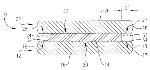
Fig. I depicts one embodiment of a stack 10 of two reversably bonded wafers.
Suitable
methods of forming such a stack are disclosed in U.S. Patent No. 2009/0218560,
filed January 23,
2009, incorporated by reference herein in its entirety to the extent not
inconsistent with the present
application. It will be appreciated that the order of assembling or applying
the components to form
the wafer stack 10 will vary, as disclosed in U.S. Patent App. Pub. No.
2009/0218560, and can be
performed in any order suitable to achieving the stack 10, as depicted in Fig.
1.
The stack structure 10 includes a first substrate 12. In this embodiment,
first substrate 12 is
a device wafer. That is, substrate 12 has a front or device surface 14, a back
surface 16, and an
outermost edge 17 defining the periphery (perimeter) of the substrate.
Although substrate 12 can be
of any shape, it would typically be circular in shape, although wafer flats
can also be used (circular
8
CA 02709626 2010-07-13
wafers having one or more straight edges on the wafer's outer perimeter).
Regardless of the shape,
the front or device surface 14 has a peripheral region 18 and a central region
20. The peripheral
region 18 preferably has a width of from about 0.05 mm to about 10 mm, more
preferably from
about 0.5 mm to about 5 mm, and even more preferably from about I mm to about
2.5 mm.
Preferred first substrates 12 include device wafers whose device surfaces
comprise arrays of
devices selected from the group consisting of integrated circuits, MEMS,
microsensors, power
semiconductors, light-emitting diodes, photonic circuits, interposers,
embedded passive devices, and
other microdevices fabricated on or from silicon and other semiconducting
materials such as silicon-
germanium, gallium arsenide, and gallium nitride. The surfaces of these
devices commonly
comprise structures formed from one ormore ofthe following materials: silicon,
polysilicon, silicon
dioxide, silicon (oxy)nitride, metals (e.g., copper, aluminum, gold, tungsten,
tantalum), low-k
dielectrics, polymer dielectrics, and various metal nitrides and silicides.
The device surface 14 can
also include raised structures such as solder bumps and metal posts and
pillars.
The stack 10 also includes a second substrate 22. In this particular
emnbodiment, second
substrate 22 is a carrier substrate. Second substrate 22 includes a carrier
surface 24 and a back
surface 26, and an outer edge 27 defining the periphery of the substrate 22.
As was the case with
first substrate 12, second substrate 22 can be of any shape, although it would
typically be circular
in shape and/or have at least one flat. Furthermore, second substrate 22 would
preferably be sized
to be approximately equal in size to first substrate 12, so that outer edge 27
of second substrate 22
will lie along substantially the same plane as outer edge 17 of first
substrate 12. Regardless of the
shape, carrier surface 24 has a peripheral region 28 and a central region 30.
The peripheral region
28 preferably has a width of from about 0.05 min to about 10 mm, more
preferably from about
0.5 nunm to about 5 mm, and even more preferably from about 1 mm to about 2.5
mm.
Preferred second substrates 22 comprise a material selected from the group
consisting of
silicon, sapphire, quartz, metals (e.g., aluminum, copper, steel), and various
glasses and ceramics.
Substrate 22 can also include other materials deposited on its surface 24. For
example, silicon
nitride can be deposited onto a silicon wafer to change the bonding
characteristics of the surface 24.
In the intermediate layer between the first substrate 12 and second substrate
22, is a layer 32
of fill material adjacent to the device surface 14 and carrier surface 24,
respectively. The thickness
9
CA 02709626 2010-07-13
of layer 32 (measured at its thickest point) will depend upon the height of
the topography on the first
substrate 12, and can range between about 5 m to about 150 m. In some
embodiments, the
preferred thickness ranges from about 5 m to about 100 m, more preferably
from about 5 l.un to
about 50 m, and even more preferably from about 10 m to about 30 Etm.
In forming the stack 10, the fill material can be applied to either substrate
12 or substrate 22
via any conventional means, including spin coating, casting from solution
(e.g., meniscus coating
or roller coating), ink jetting, and spray coating. It is preferred that the
fill layer 32 be applied so that
it has a thickness (measured at its thickest point) of from about 5 lun to
about 100 n1, more
preferably from about 5 Fun to about 50 m, and even more preferably from
about 10 m to
about 30 m. When applied via spin coating, the material forming fill layer 32
will typicallybe spin
coated at speeds of from about 100 rpm to about 5,000 rpm for a time period of
from about 15
seconds to about 300 seconds. The layer would then be baked near or above the
boiling point of the
solvent(s) present in the fill layer 32 (e.g., from about 80 C to about 250 C)
for a time period of
from about l minute to about 15 minutes to reduce the residual solvent content
in fill layer 32 to less
than about I %, by weight.
Fill layer 32 is typically formed of a material comprising monomers,
oligomers, and/or
polymers dispersed or dissolved in a solvent system. If the fill layer 32 will
be applied via spin
coating, it is preferred that the solids content of this material be from
about 1%, by weight to
about 50% by weight, more preferably from about 5% by weight to about 40% by
weight, and even
more preferably from about 10% by weight to about 30% by weight. Examples of
suitable
monomers, oligomers, and/or polymers include those selected from the group
consisting of cyclic
olefin polymers and copolymers and amorphous fluoropolymers with high atomic
fluorine content
(greater than about 30% by weight) such as fluorinated siloxane polymers,
fluorinated ethylene-
propylene copolymers, polymers with pendant perfluoroalkoxy groups, and
copolymers of
tetrafluoroethylene and 2,2-bis-trifluoromethyl-4,5-difluoro-1,3-dioxole being
particular preferred.
It will be appreciated that the bonding strength of these materials will
depend upon their specific
chemical structures and the coating and baking conditions used to apply them.
Examples of suitable solvent systems for cyclic olefin polymers and copolymers
include
solvents selected from the group consisting of aliphatic solvents such as
hexane, decane, dodecane,
CA 02709626 2010-07-13
and dodecene; alkyl-substituted aromatic solvents such as mesitylene; and
mixtures thereof. Suitable
solvent systems for amorphous fluoropolymers include fluorocarbon solvents
sold, for example, by
3M Corporation under the FLUORINERT 7' label.
In another embodiment, the fill layer 32 could also be formed of a polymeric
material that
contains dispersed nanoparticles. Suitable nanoparticle materials include
those selected from the
group consisting of alumina, eeria, titania, silica, zirconia, graphite, and
mixtures thereof.
The material of which fill layer 32 is formed should remain stable at
temperatures of from
about I50 C to about 350 C, and preferably from about 200 C to about 300 C.
Furthermore, this
material should be stable under the chemical exposure conditions encountered
in the particular
backside processes to which they will be subjected. Fill layer 32 should not
decompose (i.e., less
than about 1 /, weight loss) or otherwise lose its mechanical integrity, for
example, by melting, under
these conditions. The fill layer 32 also should not exhibit outgassing that
might cause the thin device
wafers to blister or deform, especially when subjected to high-vacuum
processes such as during the
deposition of CVD dielectric layers.
In this embodiment, the fill layer 32 preferably does not form strong adhesive
bonds, thus
facilitating separation later. Generally speaking, desirable materials include
amorphous polymeric
n iaterials that: (1) have low surface free energies; (2) are tack-free and
known to not bond strongly
to glass, silicon, and metal surfaces (i.e., would typically have very low
concentrations of hydroxyl
or carboxylic acid groups, and preferably no such groups); (3) can be cast
from solution or formed
into a thin film for lamination; (4) will flow under typical bonding
conditions to fill device wafer
surface topography, forming a void-free bond line between substrates; and (5)
will not crack, flow,
or redistribute under mechanical stresses encountered during backside
processing, even when carried
out at high temperatures or under high vacuum conditions. As used herein, low
surface free energy
is defined as a polymeric material or surface that exhibits a contact angle
with water of at least about
90 and a critical surface tension of less than about 40 dynes/em, preferably
less than about 30
dynes/cm, and more preferably from about 12 dynes/cm to about 25 dynes/cm, as
determined by
contact angle measurements.
Low bonding strength refers to polymeric materials or surfaces that do not
stick or can be
peeled from a substrate with only light hand pressure such as might be used to
debond an adhesive
11
CA 02709626 2010-07-13
note paper. Thus, anything with an adhesion strength of less than about 50
psig, preferably less than
about 35 psig, and more preferably from about I psig to about 30 prig would be
desirable for use as
fill layer 32. As used herein, adhesion strength is determined by ASTM
D4541/D7234. Examples
of suitable polymeric materials exhibiting the above properties include some
cyclic olefin polymers
and copolymers sold under the names APEL`' by Mitsui, TOPAS"" by Ticona, and
ZEONOR" by
Zeon brands, and solvent-soluble fluoropolymers such as CYTOP"' polymers sold
by Asahi Glass
and TEFLON' AF polymers sold by DuPont. The bonding strength of these
materials will depend
upon the coating and baking conditions used to apply them.
As shown in Fig. 1, the outermost portion of the fill layer 32 has been
removed and is only
adjacent to the central regions 20 and 30 of the device surface 14 and carrier
surface 24, respectively.
This can be accomplished by any means that will allow for removal of the
desired quantity without
damaging the first substrate 12, including dissolving the outermost portion
with a solvent that is
known to be a good solvent for the material of which fill layer 32 is formed.
Examples of such
solvents include those selected from the group consisting of aliphatic
solvents (e.g., hexane, decane,
dodecane, and dodecene), fluorocarbon solvents, and mixtures thereof. After
edge removal, the fill
layer 32 has an outermost edge 33, which is spaced a distance "D" from the
plane defined by the
outer edge 17 of the first substrate 12. "D" is typically from about 0.05 mm
to about 10 mm, more
preferably from about 0.5 mm to about 5 mm, and even more preferably from
about l min to about
2.5 mm. Contact with the edge removal solvent can be maintained for a
sufficient time to dissolve
the desired amount of fill layer 32 to achieve the desired distance "D," but
typical contact times
would be from about 5 seconds to about 60 seconds.
The outermost portion ofthe fill layer 32 can be removed either before or
after the substrates
12, 22 are bonded in face-to-face relationship with one another. If it is
removed before, the stack
10 is formed by contacting the second substrate 22 with the fill layer 32,
leaving a void between the
peripheral region 18 of the first substrate 12 and the peripheral region 28 of
the second substrate 22.
This contact is preferably carried out under heat and pressure, so as to cause
the material of which
fill layer 32 is formed to distribute substantially uniformlyalong the front
surface 14 of first substrate
12 as well as along the carrier surface 24 of second substrate 22. The
pressure and heat are adjusted
based upon the chemical make-up of fill layer 32, and will be selected such
that the distance "D"
12
CA 02709626 2010-07-13
remains substantially the same after pressing the second substrate 22 to the
first substrate 12 as
before such pressing together. That is, the fill layer 32 will experience
little to no flow into the void
where the layer was removed, and the distance "D" after pressing together will
be within about 10%
of the distance "D" prior to pressing together. Typical temperatures during
this step will range from
about 150 C to about 375 C, and preferably from about 160 C to about 350 C,
with typical
pressures ranging from about 1,000 N to about 5,000 N, and preferably from
about 2,000 N to about
4,000 N. If the outermost portion of the fill layer 32 is removed after
bonding the substrates 12, 22
in face-to-face relationship, the stack 10 is formed by contacting the second
substrate 22 with the fill
layer 32, under heat and pressure as described above. The outermost portion of
the fill layer 32 is
then removed leaving a void between the peripheral region 18 of the first
substrate 12 and the
peripheral region 28 of the second substrate 22.
Alternatively, the fill layer 32 is provided as a laminate that is adhered to
first substrate 12
under heat, pressure, and/or vacuum as necessary for the particular material
to ensure there are no
voids between the fill layer 32 and the front surface 14. The laminate is pre-
cut to the appropriate
shape (e.g., circular) or mechanically trimmed after application so that the
appropriately sized
distance "D" will be created, as discussed above.
Around the periphery of the outermost edge 33 ofthe fill layer 32 after the
outermost portion
of the fill layer 32 is removed, a bonding material forms an edge bond 34
between the first substrate
12 and second substrate 22, which will have a thickness corresponding to that
described above with
respect to fill layer 32. The edge bond 34 will be limited to the outer
perimeter of the first substrate
12 and second substrate 22 (i.e., adjacent to the peripheral regions 18 and
28, of the device surface
14 and carrier surface 24, respectively). In instances where the substrate 12
is circular in shape, the
edge bond 34 will be ring-shaped. Thus, in this embodiment, there is a non-
uniform material
distribution across the substrates 12, 22.
Again, like the removal of the outermost portion of the fill layer 32, the
edge bond 34 can
be applied either before or after the substrates 12, 22 are bonded in face-to-
face relationship to one
another. For example, where the fill layer 32 is comprised of low bonding
strength material, such
as TEFLON'W" AF, it is advantageous to apply the edge bond after application
and partial removal of
the fill layer 32, but before contacting of second substrate 22 with the fill
layer 32 to bond the
13
CA 02709626 2010-07-13
substrates. This alternative arrangement is particularly advantageous because
the coated substrate
12 could be fabricated with first substrate 12 being provided as a carrier
wafer. This substrate 12
could then be provided to an end user who would bond a device wafer to the
coated substrate 12 and
subject the resulting stack 10 to further processing. Thus, an adhesive-ready
carrier would be
available to the end user for added convenience, eliminating processing steps
for the end user.
Where the fill layer 32 and edge bond 34 are both applied before bonding the
substrates 12, 22, the
fill layer 32 and edge bond 34 can be applied to the same substrate, as
described above.
Alternatively, the fill laver 32 can be applied, and then the outermost
portion removed from one
substrate (e.g., the first substrate 12), while the edge bond 34 can be
applied to the peripheral region
28 of another substrate (e.g., the second substrate 22), such as by spin
coating. The substrates 12,
22 can then be bonded in face-to-face relationship. The edge bonding material
can be introduced
by any number of means. For example, when applied after the substrates are
bonded in face-to-face
relation ship, one suitable mechanism is the use of a needle, syringe, or tip
dispense instrument to
dispense the material into the void between the peripheral region 18 of the
first substrate 12 and the-
peripheral region 28 of the second substrate 22, while the structure 10 is
`slowly rotated until
peripheral regions are filled with the bonding material, thus forming the edge
bond 34. The edge
bond 34 may also be applied via capillary filling of void 44 or via chemical
vapor deposition. In a
further application process, a liquid (100% solids or solution), edge bonding
material can be
spin-applied onto the edge of the carrier or device wafer using an edge-
wrapping baffle system
before contacting the substrates 12 and 22. One such system is disclosed by
Dalvi-Malhotra et al,,
"Use of si lane-based primer on silicon wafers to enhance adhesion of edge-
protective coatings during
wet etching: Application of the TALON Wrap"!" process," Proceedings of SPIE,
vol. 6462, 2007,
pp. 646208-1 - 646208-7, incorporated by reference herein. The edge bond 34 is
then subjected to
the appropriate curing or hardening process (e.g., UV curing).
The materials from which edge bond 34 is formed should be capable of forming a
strong
adhesive bond with the substrates 12 and 22. Anything with an adhesion
strength of greater than
about 50 psig, preferably from about 80 psig to about 250 psig, and more
preferably from about
100 psig to about 150 prig, would be desirable for use as edge bond 34. In
addition, the adhesion
strength of the edge bond 34 is at least about 0.5 psig, preferably at least
about 20 psig, and more
14
CA 02709626 2010-07-13
preferably from about 50 psig to about 250 prig greater than the adhesion
strength of the fill layer
32. Furthermore, the material of which edge bond 34 is formed must meet the
thermal and chemical
stability requirements of backside processing, The edge bond 34 should remain
stable at
temperatures of from about 150 C to about 350 C, and preferably from about 200
C to about
300 C. Furthermore, this material should be stable under the chemical exposure
conditions
encountered in the backside processes to which the bonded stack will be
subjected. Edge bond 34
should not decompose (i.e., less than about 1 % weight loss) or otherwise lose
its mechanical integrity
at the above described backside processing temperatures. These materials also
should not release
volatile compounds that might cause blistering of thin device wafers,
especially when subjected to
high vacuum processes such as CVD dielectric deposition.
Preferred edge-sealing or edge-bonding materials include commercial temporary
wafer
bonding compositions such as the WaferBOND materials (available from Brewer
Science Inc.,
Rolla, MO), some commercial photoresist compositions, along with other resins
and polymers that
exhibit high adhesion strength to semiconductor materials, glass, and metals.
Especially preferred
are: (1) high solids, UV-curable resin systems such as reactive epoxies and
acrylics; (2) related
thermosetting resin systems such as two-part epoxyand silicone adhesives; (3)
thermoplastic acrylic,
styrenic, vinyl halide (non-lluoro-containing), and vinyl ester polymers and
copolymers along with
polyamides, polyimides, polysulfones, polyethersulfones, and polyurethanes
applied from the melt
or as solution coatings that are baked after application to dry and render the
peripheral regions 18
and 28 more dense; and (4) cyclic olefins, polyolefin rubbers (e.g.,
polyisobutylene), and
hydrocarbon-based tackifier resins. As was the case with the materials used to
form fill layer 32, it
will be appreciated that the bonding strength of edge bond materials will also
depend upon their
specific chemical structures and the coating and baking conditions used to
apply them.
In an alternative embodiment, only the edge bond 34 could be used between the
first substrate
12 and second substrate 22. That is, in lieu of the fill materials described
above, the layer
represented by the fill layer 32 in Fig. I could be empty (i.e., air). Thus,
there would be nothing but
air adjacent the central region 20 of the first substrate 12 and the central
region 30 of the second
substrate 22.
CA 02709626 2010-07-13
Referring to Fig. 2, in another method of forming the stack 10, surface
modification can be
used to alter the bonding strength interface between the bonding material(s)
and the first substrate 12
or second substrate 22, in lieu of a low bonding strength fill material in the
intermediate layer. With
reference to Figs. 2(a)-(d), with like parts being numbered as in Fig. 1, a
protective composition is
applied to the peripheral region 28 of the carrier surface 24 of the second
substrate 22 to form a layer
of a mask 36 adjacent the peripheral region 28. Thus, if the second substrate
22 is circular in shape,
the mask 36 is in the shape of a ring. A variety of suitable compositions can
be used to form the
mask 36. The mask 36 should be resistant to the solvent utilized during
surface modification and
other subsequent processing, but is also preferably formed from a composition
that can be easily
removed or dissolved from the carrier surface 24 without degrading the surface
treatment or
otherwise affecting the second substrate 22. The mask 36 is typically formed
of a material
comprising monomers, oligomers, and/or polymers dispersed or dissolved in a
solvent system.
Examples of suitable monomers, oligomers, and/or polymers include those
selected from the group
consisting of epoxies, polyamides, ethers, esters, cyclic olefin polymers and
copolymer, amorphous
fluoropolymers, and combinations thereof. Preferred compositions are selected
from the group
consisting of edge bonding materials, as described above (e.g., commercial
temporary wafer bonding
compositions, such as WaferBOND"), fill materials, as described above, and
photoresist
compositions (e.g., SU-8 2002, Microchern, Newton, MA). The mask 36 preferably
has a width of
from about 0.05 mm to about 10 mm, more preferably from about 0.5 rnm to about
5 mm, and even
more preferably from about 1 mrn to about 2.5 mm. The mask preferably has a
thickness of from
about 0.05 m to about 5 m, more preferably from about 0.5 m to about 2.5
pm, and even more
preferably from about 0.5 1rm to about l m.
As shown in Fig. 2(b), the area on the carrier surface 24 of the second
substrate 22 which is
not coated with the mask 36 is then chemically modified to obtain a low
bonding surface (i.e., a
non-stick surface or a surface to which a fill or bonding material cannot
strongly adhere). Preferably,
the central region 30 of the carrier surface 24 is the area subjected to
surface modification to provide
a low adhesive strength interface when placed in contact with the bonding
material. Suitable surface
modification may include, for example, chemical treatment of the substrate
surface 24 with a
hydrophobic solution capable of reacting with the substrate surface 24 to
reduce its surface free
16
CA 02709626 2010-07-13
energy, as described above. More preferably, hydrophobic organosilane
solutions are used.
Particularly preferred surface modifying compositions 38 are selected from the
group consisting of
(fluoro)alkyl silane (e.g., perfluoroalkyltrichlorosilane), (fluoro)alkyl
phosphonate, isocyanate silane,
acrylate silane, and combinations thereof. The surface modifying composition
38 can be applied by
any suitable method, such as by spin coating at a speed of at least about
1,000 rpm for about 100
seconds (and preferably about 2,000 rpm for about 60 seconds). Thus, the
surface modifying
composition 38 can be diluted with a solvent, such as FLUORINERT (3.M Corp.),
prior to applying
to the substrate surface 24. The second substrate 22 can then be baked to
evaporate the solvent at
about 50 C to about 150 C for about 30 second to about 5 minutes (and
preferably at about 100 C
for about 1 minute). The substrate 22 can then be rinsed with additional
solvent and baked again to
evaporate the solvent, as described above, to remove unreacted surface
modification solution 38 and
rinse the surface modification solution 38 off'of the mask 36, as shown in
Fig. 2(c). It is preferable
that the mask 36 does not react with the surface modification composition in
this embodiment, so
that the mask 36 is not also rendered "non-stick" by the surface modification.
The advantage of the
surface modification approach is that the intermediate layer can be selected
for any combination of
properties (e,g., thickness, solubility, thermal stability) other than
providing a non-stick or low
adhesive strength interface with the substrate, as described above with regard
to Fig. 1. Another
advantage is that a uniform bonding composition can be used for the entire
intermediate layer in lieu
of a separate fill material 32 and edge bond 34.
The surface 14 of the first substrate 12 (tile device wafer) is then coated
with a bonding
composition to create a bonding layer 40 on and across the surface 14, and the
first substrate 12 and
treated second substrate 22 are then bonded in aface-to-face relationship, as
shown in Fig. 2(d), with
the second substrate 22 now being on top of the stack 10. This contact is
preferably carried out
under heat and pressure, so as to cause the material of which bonding layer 40
is formed to distribute
substantially uniformly along the front surface 14 of first substrate 12 as
well as along the carrier
surface 24 of second substrate 22. More preferably, the substrates 12, 22 are
bonded under vacuum
and in a heated, pressurized chamber (preferably at from about 100 to about
300 C, for about I to
about 10 minutes, and more preferably from about 100 to about 200 C, for about
2 to about 5
minutes). In this embodiment, the mask 36 is not removed prior to bonding the
two substrates 12,
17
CA 02709626 2010-07-13
22 in face-to-face relationship. Thus, it is preferable that the protective
material used to form the
mask 36 is of the same material, or of a similar or compatible material, as
the materials from which
the bonding layer 40 are formed, so that upon bonding the substrates 12, 22 as
described above, the
mask 36 and bonding materials reflow together to form a uniform bonding layer
40, as shown in Fig,
2(d). The thickness of the bonding layer 40 will depend upon the height of the
topography on the
device wafer 12, and can range between about 5 l.Lm to about 150 tun. In some
embodiments, the
preferred thickness ranges from about 5 1u1m to about 100 pin, more preferably
from about 5 pm to
about 50 m, and even more preferably from about 10 gin to about 30 hm.
The materials from which bonding layer 40 are formed should be capable of
forming a strong
adhesive bond with the substrates 12 and 22, except where treated with the
surface modifying
composition 38. Suitable bonding materials include anything with an adhesion
strength of greater
than about 50 psig, preferably from about 80 psig to about 250 psig, and more
preferably from about
100 psig to about 150 psig. Furthermore, the material of which bonding layer
40 is formed must
meet the thermal and chemical stability requirements of backside processing.
The bonding layer 40
should remain stable at temperatures of from about 150 C to about 350 C, and
preferably from
about 200 C to about 300 C. Furthermore, this material should be stable under
the chemical
exposure conditions encountered in the backside processes to which the bonded
stack will be
subjected. The bonding layer 40 should not decompose (i.e., less than about I
% weight loss) or
otherwise lose its mechanical integrity at the above described backside
processing temperatures.
These materials also should not release volatile compounds that might cause
blistering of thin device
wafers, especially when subjected to high vacuum processes such as CVD
dielectric deposition.
Preferred bonding materials include commercial temporary wafer bonding
compositions such
as the WaferBOND"" materials (available from Brewer Science Inc., Rolla, MO),
some commercial
photoresist compositions, along with other resins and polymers that exhibit
high adhesion strength
to semiconductor materials, glass, and metals. Especiallypreferred are: (1)
high solids, UV-curable
resin systems such as reactive epoxies and acrylics; (2) related thermosetting
resin systems that cure
or crosslink upon heating, such as two-part epoxy and silicone adhesives,
cyclic olefin polymers and
copolymers with thermal catalyst initiators, and CYCLOTENE"" (Dow Chemical);
(3) thermoplastic
acrylic, styrenic, vinyl halide (non-fluoro-containing), and vinyl ester
polymers and copolymers
18
CA 02709626 2010-07-13
along with polyamides, polyimides, polysulfones, polyethersulfones, and
polyurethanes applied from
the melt or as solution coatings that are baked after application to dry; and
(4) cyclic olefins,
polyolefin rubbers (e.g., polyisobutylene), and hydrocarbon-based tackifier
resins. Thermosetting
materials also require the use of a crosslinking agent and potentially a
catalyst in the system as well
as a step to induce crosslinking, as described in more detail herein. The
foregoing n iaterials are also
useful for forming the mask 36 in this embodiment.
In the resulting stack 10, the bonding layer 40 contacts the modified central
region 30 and
the non-modified peripheral region 28 on the carrier surface 24.
Advantageously, the bonding
interface between the bonding layer 40 and the central region 30 of the
carrier surface 24 is weaker
than the bonding interface between the bonding layer 40 and the peripheral
region 28 of the carrier
surface 24. Thus, in the bonding layer 40, high adhesive strength regions "B"
and low adhesive
strength regions "b" are formed. The transition between the high adhesive
strength regions "B" and
the low adhesive strength regions "b" along the interface between the bonding
layer 40 and the
carrier surface 24 indicates the initial location of where the two substrates
12,'22 will begin to peel
apart during separation. It will be appreciated that during processing, the
width of the mask 36 can
be varied depending upon the desired size and location of the high adhesive
strength regions
Likewise, particularly when the mask 36 is formed from photoresist
compositions or other
patternable layers, the mask 36 could also be applied as a uniform layer over
the carrier surface 24,
and then patterned and developed in any number of ways (such as to form a
grid, lines, shapes, etc.).
Subsequent surface modification would result in a patterned nonstick surface
treatment,
Accordingly, the location and manner of separation of the substrates 12 and 22
can be customized
to the user's desired specifications.
Referring to Fig. 3, another alternative embodiment of the present invention
is depicted, with
like parts being numbered as in Fig. 2. As illustrated in this figure, the
substrates 12, 22, mask 36,
and bonding layer 40, are formed of the same materials as described above with
respect to Fig. 2,
except that in step (c) of Fig. 3, the mask 36 is removed from the carrier
surface 24 thereby exposing
the peripheral region 28 of the carrier surface 24, which remains untreated
with the surface
modifying composition 38. The mask 36 can be removed by solvent dissolution,
acid or base wet
development processes, or plasma etching. The first substrate 12 and treated
second substrate 22 are
19
CA 02709626 2010-07-13
then bonded in a face-to-face relationship with the second substrate 22 now
being on top in Fig. 3(d).
This contact is preferably carried out under heat and pressure, so as to cause
the material of which
bonding layer 40 is formed to distribute substantially uniformly along the
front surface 1.4 of first
substrate 12 as well as along the carrier surface 24 of second substrate 22,
so that the bonding layer
40 contacts the modified central region 30 and the non-modified peripheral
region 28 on the carrier
surface 24, as previously described, The mask 36 in this embodiment can also
be patterned as
described above, followed by surface modification and removal of the mask 36,
resulting in a
patterned nonstick surface treatment once the mask 36 is removed. Because this
mask 36 is
removed, the mask 36 can be made of any material suitable for masking and does
not have to be
compatible with the materials used to form the bonding layer 40. Likewise, the
mask 36 can be
reactive with the surface modification composition 38, as long as it can still
be removed from the
carrier surface 24 to reveal the untreated peripheral region 28 of the second
substrate 22.
Fig. 4 depicts another embodiment of forming a stack 10 in accordance with the
invention.
A bonding composition is applied to the surface 24 of the second substrate 22
to form a bonding
layer 40. The bonding layer 40 can be formed of any suitable materials, as
previously described with
regard to Fig, 2, although thermosetting materials are particularly preferred.
The thickness of the
bonding layer 40 will depend upon the height ofthe topography on the first
substrate 12, and can
range between about 5 m to about 150 nn. In some embodiments, the preferred
thickness ranges
from about 5 m to about 100 m, more preferably from about 5 }urn to about 50
m, and even more
preferably from about 10pnn to about 301un. A layer of fill material is
applied to the bonding layer
40 to form a fill layer 32 as shown in Fig. 2(b). The fill layer 32 has a
thickness of from about 0.05
l.un to about 5 lrm, preferably from about 0.5 Itnn to about 2.5 pm, and more
preferably from about
0.5 nn to about 1 p.m. In this embodiment, the fill layer 32 does not form
strong adhesive bonds,
and is preferably formed ofa low bonding strength material, as described above
with regard to Fig. 1:
Thus, suitable materials for forming the fill layer 32 in this embodiment
include'compositions having
the properties described above, including cyclic olefin polymers and
copolymers sold under the
APEL" by Mitsui, TOPAS" by Ticona, and ZEONOR' by Zeon brands, and solvent-
soluble
fluoropolymers such as CYTOP V polymers sold by Asahi Glass and TEFLONW' AF
polymers sold
CA 02709626 2010-07-13
by DuPont. Although it will be appreciated that the bonding strength of these
materials will depend
upon the coating and baking conditions used to apply them.
Next, as shown in Fig. 4(c), the outermost portion fill layer 32 is removed.
This can be
accomplished by any means that will allow for removal of the desired quantity
without damaging
the integrity of the bonding layer 40, including dissolving the outermost
portion with a solvent that
is known to be a good solvent for the material of which fill layer 32 is
formed. Examples of such
solvents include those selected from the group consisting of aliphatic
solvents (e.g., hexane, decanc,
dodecane, and dodecene), fluorocarbon solvents, and mixtures thereof. After
edge removal, fill layer
32 has an outermost edge 33, which is spaced a distance "D" from the plane
defined by the outermost
edge 27 of the second substrate 22. "D" is typically from about 0.05 mm to
about 10 mm, preferably
from about 0.5 mm to about 5 mm, and more preferably from about I mm to about
2.5 mm. Contact
with the edge removal solvent can be maintained for a sufficient time to
dissolve the desired amount
of fill layer 32 to achieve the desired distance "D," but typical contact
times would be from about
5 seconds to about 120 seconds.
Referring to Fig. 4(d), the second substrate 22 is bonded in face-to-face
relationship with the
first substrate 12. This contact is preferably carried out under heat and
pressure, so as to cause the
material of which bonding layer 40 is formed to reflow around the fill layer
32 and into the space left
by the edge removal process so as to contact uniformly the peripheral region
18 of the front surface
14 of the first substrate 12. More preferably, the substrates 12, 22 are
bonded under vacuum and in
a heated, pressurized chamber (preferably at from about 100 to about 300 C,
for about 1 to about
10 minutes, and more preferably from about 100 to about 200 C, for about 2 to
about 5 minutes).
In this embodiment, the bonding layer 40 can be formed from a composition that
cures or crosslinks
upon heating, such as an epoxy-based photoresist composition. Thus, in one
aspect, after contacting
the first substrate 12 and second substrate 22 under heat and pressure, the
stack 10 is then exposed
to radiation (i.e., light) to initiate crosslinking (curing) of the layer 40,
followed by a post-exposure
bake (PEB) at a temperature of from about 75 C to about 300 C, more
preferably from about 100 C
to about 250 C, and more preferably from about 100 C to about 175 C, for a
time period of from
about 15 seconds to about 120 seconds. Thus, the materials used to form the
bonding layer 40 in this
embodiment, will comprise a crosslinking agent, and optionally a catalyst in
the system.
21
CA 02709626 2010-07-13
Advantageously, the bonding interface between the central region 20 of the
device surface
14 and the fill layer 32 is weaker than the bonding interface between the
bonding layer 40 and the
peripheral region 18 of the device surface 14. Thus, high adhesive strength
regions "B" and low
adhesive strength regions "b" are formed. The transition between the high
adhesive strength regions
B and the low adhesive strength regions b along the interface between the
front surface 14 of the first
substrate 12, and the bonding layer 40 and fill layer 32 indicates the initial
location where the two
substrates 12, 22 will begin to peel apart during separation.
Referring to the stacks formed in Figs. 1, 2(d), 3(d), and 4(d), at this
stage, the first substrate
12 in the stack 10 can be safely handled and subjected to further processes
that might otherwise have
damaged the first substrate 12 without being bonded to the second substrate
22. Thus, the first
substrate 12 of the structure 10 can safely be subjected to backside
processing such as back-grinding,
CMP, etching, metal and dielectric deposition, patterning (e.g.,
photolithography, via etching),
passivation, annealing, and combinations thereof, without separation of
substrates 12 and 22
occurring, and without infiltration of any chemistries encountered during
these subsequent
processing steps into central regions 20 and 30 between substrates 12 and 22.
Advantageously, the dried or cured layers of the stacked structure 10 in this
and all
embodiments will possess a number of highly desirable properties. For example,
the layers will
exhibit low outgassing during heating and/or vacuum deposition processes. That
is, baking at about
150-300 C for up to about 60 minutes results in a film thickness change of
fill layer 32 and edge
bond 34 of less than about 5%, preferably less than about 2%, and even more
preferably less than
about 1.0%. The dried layers can also be heated to temperatures of up to about
350 C, preferably
up to about 320 C, and more preferably up to about 300 C, without chemical
reactions occurring
in the layer. In some embodiments, the layers in the bonded stack can also be
exposed to polar
solvents (e.g.,N-methyl-2-pyrrolidone) at a temperature ofabout 80 C for about
15 minutes without
reacting or dissolving.
The bond integrity of edge bond 34 or the bonding layer 40 can be maintained
even upon
exposure to an acid or base. That is, a dried edge bond 34 having a thickness
of about 15 n1 can
be submerged in an acidic media (e.g., concentrated sulfuric acid) at room
temperature for about 10
minutes or in a basic media. (e.g., 30 wt. % KOH) at about 85 C for about 45
minutes while
22
CA 02709626 2010-07-13
maintaining bond integrity. Bond integrity can be evaluated by using a glass
carrier substrate and
visually observing the edge bond 34 through the glass carrier substrate to
check for bubbles, voids,
etc.
Once the desired processing is completed, first substrate 12 and second
substrate 22 can be
readily separated. Although the edge bond 34 or the peripheral region
(corresponding to "B") of
bonding layer 40 can be maintained intact prior to separation of the
substrates 12, 22, in a preferred
method, the edge bond 34 or the peripheral region "B" of bonding layer 40 is
first chemically,
mechanically, acoustically, or thermally softened, dissolved, or disrupted to
allow the wafers to be
easily separated with very low forces at about room temperature (--- 23'-'C).
For example, the edge
bond 34 or peripheral region of bonding layer 40 is first dissolved with the
aid of a solvent or other
chemical agent. This can be accomplished by immersion in the solvent, or by
spraying a jet of the
solvent onto edge bond 34 or peripheral region of bonding layer 40 in order to
dissolve it. The use
of thermoplastic materials is especially desirable if solvent dissolution is
to be used to disrupt the
edge bond 34 or bonding layer 40. Solvents that could typically be used during
this removal process
include those selected from the group consisting of ethyl lactate,
cyclohexanone, N-methyl
pyrrolidone, aliphatic solvents (e.g., hexane, decane, dodecane, and
dodecane), and mixtures thereof.
The edge bond 34 or peripheral region of bonding layer 40 is preferably at
least partially (about 50`%x)
removed, and more preferably substantially (about 55%) removed with the
solvent.
The substrates 12 and 22 can also be separated by first mechanically
disrupting or destroying
the continuity of the edge bond 34 or peripheral region of the bonding layer
40 using laser ablation,
plasma etching, water jetting, or other high energy techniques that
effectively etch or decompose the
edge bond 34 or peripheral region of the bonding layer 40. It is also suitable
to first sever the edge
bond 34 or peripheral region of the bonding layer 40 with a fracture or break,
or to saw or cut
through or cleave the edge bond 34 or peripheral region of the bonding layer
40 by some equivalent
means.
Regardless of which of the above means is utilized, a low mechanical force
(e.g., finger
pressure, gentle wedging) can then be applied to completely separate the
substrates 12 and 22.
Advantageously, the first substrate 12 and second substrate 22 can be
separated using a peeling
motion, so that one of the substrates 12 or 22 is peeled away from the stack.
To initiate peeling a
23
CA 02709626 2010-07-13
force is applied to a portion (e.g., less tha~n'i , preferably less than 1/3,
more preferably less than 1/4,
and even more preferably less than 11110) of the periphery of the substrate to
be separated. As
discussed above, the location of initial separation will depend upon the
location of the transition of
the between the high adhesive strength regions "B" and the low adhesive
strength regions "b" along
the interface between the bonding and/or fill layers and the substrate
surface. As the initial portion
of the periphery of the substrate is lifted or pushed further upwards, the
location of the bend of the
substrate moves gradually along the interface between the substrate surface
and the bonding and/or
fill layers from the initial portion of the periphery where the force is
applied until eventually the
entire surface of the substrate has been separated from the stack. To
facilitate separation, the stack
can be simultaneously moved away (i.e,, lowered downwardly) while the force is
being applied to
the substrate to be separated, preferably in an upwards direction. The amount
of force applied to the
periphery of the substrate will vary, but preferably range between about 0.25
Newtons to about 100
Newtons, more preferably from about 2 Newtons to about 75 Newtons, and even
more preferably
to about 5 Newtons to about 50 Newtons, as measured at the portion of the
periphery of the substrate
where force is applied.
In a preferred method, an annular clamp 41 is provided in the form of a split
ring clamp for
separating the substrates 12, 22. Referring to Fig. 5(a), the ring clamp 41
has a planar body 42 with
a substantially circular shape defining the periphery and a central opening
43. Preferably, the ring
clamp body 42 is unitarily-formed, with a split at one location to form two
free ends 44a, 44b,
preferably in the form of shoulders. The term "unitarily formed" as used
herein is interchangeable
with the term "integrally formed" and means that such unitarily formed parts
are "integral" and are
not attached to each other in a separate step or detachable from each other,
but are formed from a
single piece of material. Suitable materials for the ring body 42 are selected
from the group
consisting of metals, ceramics, polymers, composites, and combinations
thereof. The ends 44a, 44b
are either moved away from one another (i.e., spread apart) in the open
configuration or drawn
toward one another in the closed configuration to compressively engage the
wafer to be separated
from the stack 10. That is, the free ends 44a, 44b are adapted to be clamped
in proximal relationship
so that the ring fits around the circumference (periphery) of the wafer.
Preferably, in the closed
configuration, the ends 44a, 44b are urged toward one another, but remain
unjoined (i.e., a gap
24
CA 02709626 2010-07-13
between the ends remains and the ring forms a discontinuous circular body),
although the ends 44a,
44b can be joined to form a gap-free continuous shape. In use, the drawing
together or spreading
apart of the ends 44a, 44b causes the central opening 43 to be reduced or
enlarged to effect the
clamping action of the body 42 around the wafer to be separated from the stack
10, and permits for
accommodation of various-sized wafers, while maintaining even pressure
throughout the
circumference (periphery) of the wafer where engaged by the ring. In another
embodiment, the ring
clamp 4l could be a multi-piece system, with each piece being unitarily
formed. The pieces are
brought together to form the ring around the circumference of the wafer
engaging it as described
above. The multi-piece system can comprise from about 2 to about 25 pieces,
more preferably from
about 2 to about 10 pieces, even more preferably from about 2 to about 4
pieces, and most preferably
about 2 pieces. Advantageously, regardless of the embodiment, the ring clamp
41 does not need to
engage all 360 of the periphery ofthe substrate to effectively separate the
stack. Rather, the ring
clamp body 42 is suitable for use with wafer flats having one or more flat
edges, as explained in
more detail below.
Referring to Fig. 6(a), the ring clamp body 42 has an annular interior
sidewall 45 defining
the inner diameter "d" of the ring body 42, and an annular exterior sidewall
46 defining the outer
diameter "D" of the ring body 42. The inner diameter "cr' ranges from about I
0 rum to about
400 mm, preferably from about 75 mm to about 350 mm, and more preferably from
100 mm about
to about 275 mm. The outer diameter "D" ranges from about 25 mm to about 550
mm, preferably
from about 100 mm to about 400 nom, and more preferably from about 250 mm to
about 350 mm.
However, it will be appreciated that the ring body 42 can be of virtually any
size depending upon the
size of the wafer to be separated. The interior sidewall 45 and exterior
sidewall 46 are substantially
parallel to one another. The ring body 42 has a width "J4/," as measured from
the interior sidewall
45 to the exterior sidewall 46, of from about 0.1 to about 50 mm, preferably
from about 0.5 to about
25 mm, and more preferably from about I to about 12 mm. The interior sidewall
45 also has a
thickness "t," which ranges from about 0.1 to about 15 mm, more preferably
from about 0.5 to about
10 mm, and even more preferably from about I to about 5 nun. The exterior
sidewall 46 has a
thickness "T," which preferably ranges from about 0.15 to about 16 nun, more
preferably from about
0.55 to about 11 mm, and even more preferably from about 1.5 to about 6 mm.
The ratio of t:T will
CA 02709626 2010-07-13
preferably be from about 1:20 to about 1:1, more preferably from about 1 :10
to about 1:5, and even
more preferably about 2:3.
The ring body 42 also has a top surface 48 extending between the interior
sidewall 45 and
exterior sidewall 46, and a wafer-engaging surface 50 extending from the
interior sidewall 45
outwardly in substantially parallel alignment with the top surface 48. The
wafer-engaging surface
50 does not extend all of the way to the exterior sidewall 46, but terminates
at a point p" that is
spaced from the exterior sidewall 46 at a width "w," as measured from that
point "p" to the external
sidewall 46. The width uu' ranges from about 0.01 to about 45 mm, preferably
from about 0. 1 to
about 20 mm, and more preferably from about 0.5 to about 10 mm. The ring body
42 has all
inwardly extending annular ridge 52, which slopes inward and downward from
point "pp" of the
wafer-engaging surface 50, and away from the plane defined by the top surface
48 and wafer-
engaging surface 50, terminating in a free edge 54. The ridge 52 has a sloped
shoulder surface 56
extending between the free edge 54 and the point "p" where the wafer-engaging
surface 50
terminates in the ring body 42. Thus, the outwardly extending wafer-engaging
surface 50 and
inwardly and downwardly extending annular ridge 52 cooperatively form an
annular wafer-receiving
groove 58 at an acute angle (0). Preferably, the groove angle (0), as measured
from the wafer-
engaging surface to the shoulder surface, is from about 10 to about 90 ,
preferably from about 20
to about 75 , and more preferably from about 30 to about 60 . The annular
ridge 52 also has all
underside surface 60, which preferably extends parallel to the planes defined
bythe wafer-engaging
surface 50 and the top surface 48: The ring body 42 also has a bottom surface
62, which slopes
downward and away from the plane defined by the top surface 48, extending
between the exterior
sidewall 46 and the underside surface 60 of the annular ridge 52.
The free edge 54 of the annular ridge 52 preferably does not extend inward
past the plane "P"
defined by the interior sidewall 45. Thus, the annular ridge 52 and groove 58
are outvi'ardly offset
from the interior sidewall 45, so that when a wafer is received in the groove
58, the backside surface
26 of the wafer is engaged by the wafer-engaging surface 50 of the ring body
42, and the outer edge
27 and peripheral region 28 of the wafer are engaged by the shoulder 56 and
free edge 54 of the ridge
52. This is shown in Fig. 6(b) using the second substrate 22 as an example.
The ring clamp 42 is
then moved into the close configuration, thereby retaining the wafer 22 in the
groove 58. More
26
CA 02709626 2010-12-23
pccificalfy, at least a portion of the periphery of the wafer 22 is received
in the groove 58. Where
the water edge 27 is rounded or beveled, the shoulder 50 and free edge 54
engage the rounded corner
)I'the wafer created by the water edge 27 and the peripheral region 28.
designated by" v."
In an alternative embodiment of the invention, as shown in Fig. 5(b), the
clamp body42 does
not have a central opening 43. Rather, the void corresponding to the central
opening 43 depicted in
the Figs. 5(a) cued 6(a) is solid and the clamp body 42 is disc-shaped.
Accordingly, as shown in Figs.
5(h) and 6(c), the top surface 48 extends the entire diameter "D" between the
exterior sidewall 46,
and the wafer-engaging surface 50 extends the entire distance between point
"p."
In use. referring to Fig. 7, stack 10 is placed on a chuck 64 capable of
providing adequate
I U iwld-down force to secure the first substrate 12 during subsequent steps.
The chuck 64 could use
vacuum force. electrostatic force. magnetic force. mechanical force. physical
restraint, or any other
Suitable means that would provide proper hold-down force while providing
support for the first
substrate 12 wittte.,ut causing damage. The ring clamp body 42 is placed about
the periphery of the
;second substrate 22, so that the substrate 22 is received in the wafer-
receiving groove 58, as
I5 described above. The free ends 44a. 44b of the body 42 are drawn towards
one another to
compressively engage the periphery of the second substrate 22 (not shown). The
ring clamp 41
prelerably provides even pressure throughout the circumference of the second
substrate 72, except
in embodiments where the second substrate 22 is a water flat. In that case,
one portion of the
periphery (i.e., the flat side) of the wafer is not engaged by the clamp. As
noted above, the ring
20 clamp does not need to engage all 360 of the periphery (circumference) of
the substrate to
effectively separate the stack 10. Rather. it is suitable tier the ring clamp
to engage only about I of
the periphery of the substrate 22 for effective separation. More specifically,
the ring clamp
preferably engages at least about 25' of the substrate periphery, more
preferably from about 45 to
about 90", and even more preferably from about 90 to about 180 of the
substrate periphery. When
25 a wafer flat is used. the flat edge is faced away from the initial peel
location, such that the flat edge
is the fast portion of the wafer to be detached during the dcbonding step.
Importantly, the ring clamp body 42, when clamped, engages only the second
substrate 22,
and stakes no contact with the first substrate 12. Thus, when the first
substrate 12 is a device wafer.
the inventive method and apparatus permits effective separation of the stack
10 without inflicting
,7
CA 02709626 2010-07-13
any mechanical force or stress on the device wafer, minimizing the risk of
breaking or damaging the
device. As explained above, the edge bond 34 or peripheral region of the
bonding layer 40 is
preferably partially or substantially removed prior to separation of the
substrates. However, the edge
bond 34 or peripheral region of the bonding layer 40 does not have to be
removed. Thus, where the
edge bond 34 or peripheral region of the bonding layer 40 is present, the ring
clamp body 42 may
also make contact with edge bond 34 or peripheral region of the bonding layer
40.
In an alternative embodiment, shown in Fig. 8, a layer of an adhesive film or
tape 66 is
applied adjacent the chuck 64 to secure the first substrate 12 to the chuck
64. The stack 10 is then
placed adjacent the adhesive film layer 66. Suitable materials for the
adhesive film or tape layer 66
include those having relatively low adhesion, no adhesive transfer, and the
ability to stretch without
tearing. Preferably, the adhesive film layer 66 is formed using dicing tape,
which is typically used
in the art to temporarily support device substrates for handling purposes
during low-temperature
operations. Here, the adhesive film layer 66 provides additional support for
the first substrate 12
after separation, particularly where the device substrate 12 has delicate
features built on it or has
been thinned. Preferred dicing tapes are selected from the group consisting of
poly vinyl chloride,
polyethylene, polyolefin, and combinations thereof. The adhesive film layer 66
preferably has a
thickness of from about 0.01 to about 3 mm, more preferably from about 0.05 to
about I mm, and
even more preferably from about 0.07 to about 0.2 min.
Referring to Fig. 9, regardless of the embodiment, a force (preferably upward)
is applied to
only a portion (e.g., less than ',/z, preferably less than 1/3, more
preferably less than 1/4, and even
more preferably less than 1 / 10) of the periphery of the ring clamp body 42
during separation, thereby
lifting the corresponding portion of the periphery of the second substrate 22,
defined by edge 27,
in a direction away from the device wafer 12 beginning at the peripheral
region 28 of the substrate
22. The amount of force applied to the edge of the substrate will vary, but
preferably range between
about 0.25 Newtons to about 100 Newtons, more preferably from about 2 Newtons
to about 75
Newtons, and even more preferably to about 5 Newtons to about 50 Newtons, as
measured at the
edge of the substrate. Thus, the second substrate 22 is separated from the
stack 10 via a peeling
motion, as previously described. It will be appreciated that the location of
initial separation depicted
in Fig. 9 is by way of example only, and that the actual location
of'separation will depend on the
28
CA 02709626 2010-07-13
materials and surface treatments (if any) used to form the stack, as described
above, including the
location and/or pattern of the non-stick surface modification or low strength
bonding layers included
in the stack. As previously explained, the location of adhesive failure, which
will determine the
initial location of separation, can be modified as desired by the end user.
Furthermore, the ring body 42 is preferably flexible so that when the portion
of the periphery
of the ring clamp 41 is raised, the body 42 in that location flexes or bends,
preferably upward, with
the force. This deflection in the ring body 42 causes the corresponding
portion of the periphery of
the substrate 22 to likewise bend or deflect at an angle away from the stack
10. That is, as shown
in Fig. 9, when one portion of the periphery of the ring body 42 is raised,
the opposite portion of the
ring body 42 preferably remains substantially stationary and does not press
downward on the
stack 10 in response to the other portion being raised. To further facilitate
separation, the chuck 64
securing the first substrate 12 can be gradually moved away from the second
substrate 22 during
separation, and is preferably lowered downward. The lowering of the chuck 64
can be done
simultaneously with the applying of force to the ring clamp 42. Alternatively,
the force on the
second substrate 22 and the resulting peeling motion is effected by the
movement of the chuck 64
away from the second substrate 22, which is held substantially stationary as
the stack 10 is pulled
away.
Advantageously, and unlike prior art bonding methods, separation does not
require
overcoming strong adhesive bonds between the fill layer 32, edge bond 34, or
bonding layer 40 and
the entire surface of substrate 12 or substrate 22. Instead, it is only
necessary to release the adhesive
bonds at edge bond 34 or peripheral region of the bonding layer 40 in contact
with the peripheral
regions 18 and 28 for separation to occur. Once separated, the surface of the
first substrate 12 can
then be rinsed clean with appropriate solvents or any other wet or dry etch
techniques as necessary
to remove residual edge bond 34, fill layer 32 or bonding layer 40 materials,
as applicable.
In another embodiment. depicted in Fig. 10, with like numbering being used for
like parts,
the ring clamp 42 is replaced with a flexible chuck 68 having a periphery. The
flexible chuck is
capable of providing adequate pulling force to secure the second substrate 22
during subsequent
steps. This flexible chuck 68 could use vacuum force, electrostatic force, or
any other suitable
means that would provide proper force while providing support for the second
substrate 22 without
29
CA 02709626 2010-07-13
causing damage while still allowing it to bend to create the peeling motion.
Suitable materials for
the flexible chuck 68 including those selected from the group consisting of
silicones, polyimides,
polyamides, olefins, fluoro polymers, nitriles, other rubbers, and any other
flexible materials. As
with the ring clamp embodiment, an adhesive film 66 could also be used to
support the first substrate
1 2 in the stack, as shown in Fig. 1 1. In either embodiment, a force is then
applied to a portion of the
periphery ofthe flexible chuck 68, thereby lifting the corresponding portion
of the periphery of the
second substrate 22 and removing it from the stack 10 in a peeling motion, as
described. Again, the
actual location of initial separation between materials in the peripheral
region 28 and central region
30 of the substrate 22 depends on the materials used and location of the
surface treatment (if any),
fill layer 32, edge bond 34, and/or bonding layer 40. The first substrate 12
can then be rinsed clean
with appropriate solvents as necessary to remove residual edge bond 34, fill
layer 32, or bonding
layer 40 materials, as applicable. Advantageously, where the first substrate
12 is a device wafer,
there is no mechanical force or stress applied to the device wafer in the
inventive separation method,
minimizing the risk of breaking or damaging the wafer during separation.
In yet another embodiment, shown in Fig. 12, the ring clamp 42 is replaced
with an adhesive
film 70 that is capable of providing adequate pulling force to secure the
second substrate 22 during
subsequent steps. This adhesive film 70 could consist of a range of backing
materials and adhesives
from high bond strength to low bond strength and a variety of supporting
strengths that is capable
of providing adequate holding force to overcome the bond forces created in
central region 30 and
p
eripheral region 28 while providing limited support for the second substrate
22 without causing
r CD
damage while still allowing it to bend to create the peeling motion. Preferred
materials for the
adhesive film 70 include poly vinyl chloride, polyethylene, polyolefin, and
combinations thereof
The adhesive film 70 preferably has a thickness of from about 0.01 to about 3
mm, more preferably
from about 0.05 to about 1 mm, and even more preferably from about 0.07 to
about 0.2 nun. As with
the ring clamp embodiment, an adhesive film 66 could also be used to support
the first substrate 12
in the stack, as shown in Fig. 13. In either embodiment, a force is applied to
a portion of the
periphery of the adhesive film 70 to lift the corresponding portion of the
periphery of the second
substrate 22, thus removing it from the stack 10 in a peeling motion, as
described. Again, the actual
location of initial separation between materials in the peripheral region 28
and central region 30 of
CA 02709626 2010-07-13
the substrate depends on the materials used and location of the surface
treatment (if any), fill layer
32, edge bond 34, and/or bonding layer 40.
While the above describes the primary method of practicing the present
invention, there are
several alternative embodiments of the invention. For example, the above
embodiments described
the first substrate 12 as a device wafer and the second substrate 22 as a
carrier substrate. It is also
acceptable that first substrate 12 is the carrier substrate and second
substrate 22 is the device wafer.
In that instance, front surface 14 of first substrate 12 will not be a device
surface, but rather will be
a carrier surface. Also, surface 24 of second substrate 22 will not be a
carrier surface, but instead
will be a device surface. In other words, the fill layer 32 can be applied to
the carrier rather than the
device wafer, or the surface treatment 38 can be carried out on the device
wafer rather than the
carrier, with the same quality of stacked structure 10 being formed during the
subsequent bonding
step. In addition, although the embodiments of Figs.7-1 3 depict the stack 10
with the edge bond 34
or peripheral region of the bonding layer 40 removed, the edge bond 34 or
peripheral region of the
bonding layer 40 does not have to be removed prior to effecting separation of
the wafers.
Furthermore, in lieu of the sequential application of the fill layer 32, edge
bond 34, surface
modification 38, and/or bonding layer 40 to the same substrate 12, it is also
suitable to apply the fill
layer 32, edge bond 34, surface modification 38, and/or bonding layer 40 to
the first substrate 12, and
the other of fill layer 32, edge bond 34, surface modification 38, and/or
bonding layer 40 to the
second substrate 22. The first and second substrates 12, 22 could then be
pressed together in a face-
to-face relationship under heat and/or pressure as described above in order to
bond the two.
Finally, while in some embodiments it is preferred that the fill layer 32 does
not form strong
adhesive bonds with either device surface 14 or carrier surface 24, in other
embodiments it may be
desirable to formulate fill layer 32 so that it does not form strong adhesive
bonds with only one of
device surface 14 or carrier surface 24. As was also the case with the
embodiments previously
discussed, the substrates 12 and 22 could be reversed so that first substrate
1.2 would be the carrier
substrate and second substrate 22 would be the device wafer. Again, in this
instance, front
surface 14 of first substrate 12 will not be a device surface, but rather will
be a carrier surface. Also,
surface 24 of second substrate 22 will not be a carrier surface, but instead
will be a device surface.
31
CA 02709626 2010-07-13
It will be appreciated that the mechanism for hardening or curing these
materials can be
readily selected and adjusted by those of ordinary skill in the art. For
example, in some
embodinments, it may be desirable to use a non-curing composition for easier
dissolving in later
removal and cleaning processes. For each of these materials, thermoplastic or
rubber-like
compositions (typically having a weight average molecular weight of at least
about 5,000 Daltons),
resin- or rosin-type compositions (typically having a weight average molecular
weight of less than
about 5,000 Daltons), and mixtures of the foregoing Would be suitable.
It will be appreciated that the above can be used to fabricate a number of
integrated
microdevices, including those selected from the group consisting of silicon-
based semiconductor
devices, compound semiconductor-based devices, arrays of embedded passive
devices (e.g.,
resistors, capacitors, inductors), MEMS devices, microsensors, photonic
circuit devices, light
emitting diodes, heat management devices, and planar packaging substrates
(e.g., interposers) to
which one or more of'the foregoing devices has been or will be attached.
1.5
EXAMPLES
The following examples set forth preferred methods in accordance with the
invention. It is
to be understood, however, that these examples are provided by way of
illustration and nothing
therein should be taken as a limitation upon the overall scope of the
invention.
EXAMPLE I
Separation of Fdge-Bonded Wafers having Modified Center Surface Using 1-land-
Operated
Peeler with Removal of Bonding Material from the Outer Edge
In this procedure, a wafer stack is prepared according to a method of the
invention and then
separated using a hand-operated peel separator. Prior to adhering the two
wafers together, the center
contact surface of one wafer is chemically modified using a fluorinated silane
solution to create an
adhesive strength differential across the wafer surface. A bonding material
(WafcrBOND"' HTI 0.10,
available from Brewer Science, Inc., Rolla, MO) was dispensed onto the surface
ofa 200-mm silicon
wafer (wafer 1) at the outer edge to form a very thin coating around the
peripheral region of the
32
CA 02709626 2010-07-13
wafer surface that was about 2.5 mm wide by approximately 0.5 h.m thick. A
surface-modifying
composition was formed by diluting a fluorinated silane ((heptadecafluoro-
1,1,2,2-tetrahydradecyl)
trichlorosilane; Gelest Inc., Morrisville, PA) to a 1% solution using FC-40
solvent (perfluoro
compound with primarily C12, sold under the name FLUORINER'I'"", obtained from
AMS Materials
LLC, Jacksonville, FL). The resulting solution was spin coated onto the
surface of wafer 1, followed
by baking on a hot plate at l 00 C for 1 minute. The wafer was then rinsed
with additional FC-40
solvent in a spin coater to remove unreacted silane from the center surface,
and baked at 100 C for
an additional 1 minute. The bonding material prevented the surface-modifying
composition from
coming into contact with the edge of wafer I leaving it untreated while the
center section was
treated. The bonding material does not react with the silane, which is washed
away during the
rinsing step, and thus the surface of the bonding material also remains
untreated. The bonding
material was allowed to remain on the edge of wafer I for subsequent
processing steps (i.e., was not
removed prior to adhering the wafers).
Next, the surface of another 200-mnm silicon wafer (wafer 2) was coated with
the same
bonding composition (WaferBOND"' HT10.10) via spin coating to a layer having a
thickness of
about 15 [um. Wafer 2 was then baked at 110 C for 2 minutes, followed by 160 C
for an additional
2 minutes. The coated wafers were then bonded in a face-to-face relationship
under vacuum in a
heated vacuum and pressure chamber at 220 C and 15 prig for 3 minutes, so that
the bonding
material on wafer I and the bonding material on wafer 2 reflowed together to
create one bonding
layer.
Next, to remove the peripheral edge of the bonding layer, the bonded wafers
were soaked in
the bonding material's remover (WaferBOND`i Remover, available from Brewer
Science, Inc., Rolla,
MO) for about 1 hour to remove the bonding material from the outer zone. The
removal process is
complete once the removal process reaches the fluorinated silane coating in
the center of wafer 1.
The removal time period will vary depending upon the thickness of the bonding
layer, and can be
determined empirically, In general, the thicker the bonding layer, the faster
the removal rate due to
the larger space between the wafers allowing for greater solvent contact.
Advantageously, the treated
center surface is also hydrophobic, so the solvent will also effectively stop
wetting through the layer
once it reaches the center. Ideally, complete removal of the edge portion of
the bonding layer occurs,
33
CA 02709626 2010-07-13
however, it is only necessary to cleave the layer laterally around the edge of
the bonding layer (i.e.,
create a gap) for effective separation of the wafers. Thus, some bonding
material residue on the
peripheral edge of wafer 1 and wafer 2 is acceptable.
The resulting stacked wafers were then separated using a ring clamp (see Fig.
5(a)), with a
handle attached to the free ends for hand-operated separation. Wafer 2 was
held in place by a
vacuum chuck, and the retaining ring of the ring clamp was placed
circumferentially about the
periphery of wafer 1, with the ends of the ring being clamped in proximal
relationship to provide
even pressure around the edges of the wafer (i.e., throughout the wafer's
circumference). The handle
attached to the ring clamp was then tilted so that the free edge of the handle
lifts upwards away from
the transverse plane of the stack, causing the ring clamp to deflect, thereby
lifting the edge of wafer
I up and away from wafer 2 in a peeling motion. After the separation, the only
residue of the
bonding composition coating on wafer 1 was on the peripheral region (2.5 mm
wide untreated
surface) of wafer 1. There was no transfer of bonding material to the treated
center surface of wafer
1. The bonding material coating remained on wafer 2 in the center, with
residue at the peripheral
region. Either wafer in this example could be considered the device wafer or
the carrier wafer.
EXAMPLE 2
Separation o/'Adhered kVaJer- Slack Using Hand-Operated! Peel Separator
In this procedure, a wafer stack is prepared according toanother method of the
invention and
then separated using a hand-operated peel separator. Prior to adhering the two
wafers together, the
center surface of one silicon wafer is chemically modified using a fluorinated
silane solution to
create an adhesive strength differential across the wafer surface. To modify
the center surface of the
wafer, the edge of the wafer was first masked using a coating of an epoxy-
based photoresist (SU-8
2002, Microchem, Newton, MA). The photoresist composition was dispensed onto
the outer edge
surface of a 200-ram silicon wafer (wafer I) to coat a peripheral ring-shaped
section of the wafer
surface that was about 2.5 mm wide.
Next, a fluorinated silane ((hepta-decafluoro-1,1,2,2-tetrahydradecyl)
trichlorosilane; Gelest,
Morrisville, PA) was diluted to a l% solution using FC-40 solvent (perfluoro-
alkyl compound with
primarily C,,, sold under the name FLUORINERT`'`; obtained from AMS Materials
LLC, Jackson,
34
CA 02709626 2010-07-13
FL). The diluted solution was spin coated onto the surface of wafer 1. The
wafer was baked on a
hot plate at 100 C for 1 minute, and then rinsed with FC-40 solvent in a spin
coater, followed by
baking at 100 C for an additional 1 minute. The epoxy-based photoresist mask
was then removed
using acetone in a spin coater to expose the untreated edge of the wafer.
Thus, only the center
portion of wafer I was treated with the fluorinated silane solution and
rendered "non-stick," while
the edges of the wafer retained a bondable surface.
The surface of another 200-mrn silicon wafer (wafer 2) was coated with a
bonding
composition (WaferBOND 1IT10.10) via spin coating. This wafer was then baked
at 110 C for
2 minutes, followed by 160 C for 2 minutes. The coated wafers were then bonded
in a face-to-face
relationship under vacuum in a heated vacuum and pressure chamber at 220 C and
10 psig for- 3
Minutes.
Next, the resulting stacked wafers were then separated using a ring clamp (see
Fig. 5(a)), with
a handle attached to the free ends for hand-operated separation. In this
procedure, the peripheral
region of the bonding composition is not removed prior to separation. Wafer 2
was held in place by
1.5 a vacuum chuck, and the retaining ring of the ring clamp was placed
circumferentially about the
periphery of wafer 1, with the ends of the ring being clamped together to
provide even pressure
around the edges of the wafer (i.e., throughout the wafer's circumference).
The handle attached to
the ring clamp was then tilted so that the free edge of the handle lifts
upwards away from the
transverse plane of the stack, causing the ring clamp to deflect, thereby
lifting the edge of wafer 1
up and away from wafer 2 in a peeling motion. After the separation, only about
a 2.5 mm wide ring
of the bonding composition coating transferred to the edge of wafer 1, while
the rest of bonding
composition remained on wafer 2. That is, the bonding composition only adhered
to the outer edge
surf1rce of wafer I and did not adhere to the chemically treated center
surface of wafer 1. Either
wafer in this example could be considered the device wafer or the carrier
wafer.
CA 02709626 2010-07-13
EXAMPLE 3
Hand-Operated Peel Separator used to Separate leaf 'r Stack with
Center Contact Saar%ace Coated with Release Material
In this procedure, a wafer stack is prepared according to another method of
the invention and
then again separated using a hand-operated peel separator. Prior to adhering
the two wafers together,
the center surface of one wafer is coated with a release material to create an
adhesive strength
differential across the wafer surface-center layer interface. First, a
negative epoxy-based photoresist
(sold under the name SU-8 2010; obtained from MicroChem) was spin coated onto
the entire surface
of a 200-mm glass wafer (wafer 1), followed by baking at 110 C for 2 minutes
to effect solvent
removal. A Teflon"" AF solution (Teflon'"' AF2400 in FC-40; obtained from
DuPont) was then spin
coated over the photoresist layer to create a nonstick layer. Next, FC-40
solvent was dispensed onto
the surface of the wafer at the outer edge to remove about a 1-3 mm wide
section of the Teflon"AF
coating from the peripheral edge of the wafer surface, followed by baking 110
C for 2 minutes to
remove the solvent.
The wafer was then bonded in a race-to-face relationship with a blank, 200-mm
silicon wafer
(wafer 2) under vacuum in a heated vacuum and pressure chamber at 120 C and 10
psig for 3
minutes. During this step, the photoresist layer rellows around the Teflon'
layer to fill the gaps on
the outer edge of the wafers where the Teflon layer was removed above, thus
bonding to the
peripheral edge of wafer 2. The bonded wafers were then exposed to broadband
UV light from the
outer side of the glass wafer, followed by baking at 120 C for 2 minutes to
crosslink and cure the
SU-8 2010 coating.
The resulting stacked wafers were then separated using a ring clamp (see Fig.
5(a)), with a
handle attached to the free ends for hand-operated separation. Wafer 2 was
held in place by a
vacuum chuck, and the retaining ring of the ring clamp was placed
circumferentially about the
periphery of wafer 1, with the ends of the ring being clamped together to
provide even pressure
around the edges of the wafer (i.e., throughout the wafer's circumference).
The handle attached to
the ring clamp was then lifted, causing the ring clamp to deflect, thereby
lifting the edge of wafer
I up and away from wafer 2 in a peeling motion, as described in Example 1. In
this procedure, the
peripheral region of the bonding composition is not removed prior to
separation. Rather, the
36
CA 02709626 2010-07-13
photoresist layer is laterally cleaved at the initial separation point as a
natural consequence of the ring
clamp deflection motion, so that some of the photoresist material remained on
the glass wafer (wafer
1), while the portion of the layer was transferred to the silicon wafer (wafer
2) in the untreated
region. After separation, the wafer 2 had only a ring of material at the outer
1-3 mm, while there was
no material transfer in the center region of the wafer that had been in
contact with the Teflon 'release
layer of wafer 1. Either wafer in this example could be considered the device
wafer or the carrier
wafer.
EXAMPLE 4
Nand-Operated Peel Separator used to Separate Wafer Stack with
Center SurJcrce Tilled with Material having Low Adhesion to Either Substrate
In this procedure, a wafer stack is prepared according to another method of
the invention and
then again separated using a hand-operated peel separator. Prior to adhering
the two wafers together,
the center surface of one wafer is coated with a release material to create an
adhesive strength
differential across the wafer si.rrface. The Teflon' AF solution used in
Example 3 was spin coated
onto the surface of a 200-mm silicon wafer (wafer I) to form a coating with a
thickness of about
10 gm. Next, FC-40 solvent was dispensed onto the surface of the wafer at the
outer edge to remove
about a 3-5 mm wide section ofthe Teflon`' AF coating from the wafer surface.
The wafer was then
baked at l l 0 C for 2 minutes. Next, the edge of the wafer was coated with
WaferBOND'` 1-IT 10.10
bonding composition via spin coating, with the material only being dispensed
at the edge to form a
layer of bonding material around the peripheral region of the wafer surface
that was about 3-5 min
wide by approximately 10 m thick. Thus, the Teflon" coating and bonding
material formed a
single, non-uniform layer ofmaterial across the wafer surface. The wafer was
then bonded in a face-
to-face relationship with a blank, 200-mm silicon wafer (wafer 2) under vacuum
in a heated vacuum
and pressure chamber at 220 C and 10 psig for 2 minutes.
The resulting stacked wafers were then separated using a ring clamp (see Fig.
5(a)), with a
handle attached to the free ends for hand-operated separation. Wafer 2 was
held in place by a
vacuum chuck, and the retaining ring of the ring clamp was placed
circumferentially about the
periphery of wafer 1, with the ends of the ring being clamped together to
provide even pressure
37
CA 02709626 2010-07-13
around the edges of the wafer (i.e., throughout the wafer's circumference).
The handle attached to
the ring clamp was then lifted, causing the ring clamp to deflect, thereby
lifting the edge of wafer
I up and away from wafer 2 in a peeling motion, as described in Example 1. In
this procedure, the
peripheral region of the bonding composition is not removed prior to
separation. After separation,
wafer 2 had only a ring of the bonding material on the outer 3-5 mm, while
there was no material
transfer in the center. Wafer I had a ring of bonding material on the outer 3-
5 mm and the Tcflon""
AF coating remained in the center. The bonding material had been cleaved
through its cross section
and was split between the two wafers. Either wafer in this example could be
considered the device
wafer or the carrier wafer.
38