Note: Descriptions are shown in the official language in which they were submitted.
CA 02709718 2010-06-16
WO 2009/094009 PCT/US2008/012901
1 [00011 LARGE AREA NANOPATTERNING METHOD AND APPARATUS
2 [0002] Field
3 [0003] Embodiments of the invention relate to nanopatterning methods which
can be
4 used to pattern large substrates or substrates such as films which may be
sold as rolled
goods. Other embodiments of the invention pertain to apparatus which may be
used to
6 pattern substrates, and which may be used to carry out method embodiments,
including
7 the kind described.
8 [0004] Background
9 [0005] This section describes background subject matter related to the
disclosed
embodiments of the present invention. There is no intention, either express or
implied,
11 that the background art discussed in this section legally constitutes prior
art.
12 [0006] Nanostructuring is necessary for many present applications and
industries and
13 for new technologies which are under development. Improvements in
efficiency can be
14 achieved for current applications in areas such as solar cells and LEDs,
and in next
generation data storage devices, for example and not by way of limitation.
16 [0007] Nanostructured substrates may be fabricated using techniques such as
a-beam
17 direct writing, Deep UV lithography, nanosphere lithography, nanoimprint
lithography,
18 near-filed phase shift lithography, and plasmonic lithography, for example.
19 [0008] Nanolmprint Lithography (NIL) creates patterns by mechanical
deformation
of an imprint resist, followed by subsequent processing. The imprint resist is
typically a
21 monomeric or polymeric formulation that is cured by heat or by UV light
during the
22 imprinting. There are a number of variations of NIL. However, two of the
processes
23 appear to be the most important. These are Thermoplastic Nanolmprint
Lithography
24 (TNIL) and Step and Flash Nanolmprint Lithography (SFIL).
[0009] TNIL is the earliest and most mature nanoimprint lithography. In a
standard
26 TNIL process, a thin layer of imprint resist (a thermoplastic polymer) is
spin coated onto a
27 sample substrate. Then a mold, which has predefined topological patterns,
is brought into
1
CA 02709718 2010-06-16
WO 2009/094009 PCT/US2008/012901
1 contact with the sample, and pressed against the sample under a given
pressure. When
2 heated above the glass transition temperature of the thermoplastic polymer,
the pattern on
3 the mold is pressed into a thermoplastic polymer film melt. After the sample
with
4 impressed mold is cooled down, the mold is separated from the sample and the
imprint
resist is left on the sample substrate surface. The pattern does not pass
through the
6 imprint resist; there is a residual thickness of unchanged thermoplastic
polymer film
7 remaining on the sample substrate surface. A pattern transfer process, such
as reactive
8 ion etching, can be used to transfer the pattern in the resist to the
underlying substrate.
9 The variation in the residual thickness of unaltered thermoplastic polymer
film presents a
problem with respect to uniformity and optimization of the etch process used
to transfer
11 the pattern to the substrate.
12 [00101 In the SFIL process, a UV curable liquid resist is applied to the
sample
13 substrate and the mold is made of a transparent substrate, such as fused
silica. After the
14 mold and the sample substrate are pressed together, the resist is cured
using UV light, and
becomes solid. After separation of the mold from the cured resist material, a
similar
16 pattern to that used in TNIL may be used to transfer the pattern to the
underlying sample
17 substrate. A number of challenges exist with both the SFIL and TNIL
processes,
18 including template lifetime, throughput rate, imprint layer tolerances, and
critical
19 dimension control during transfer of the pattern to the underlying
substrate. The residual,
non-imprinted layer which remains after the imprinting process requires an
additional etch
21 step prior to the main pattern transfer etch. Single field NIL has
difficulty in controlling
22 the uniformity of a replicated pattern over a large surface area substrate,
due to problems
23 in maintaining a uniform pressure over large areas. A step-and-repeat
method can
24 potentially cover large areas, but the microstructure formed in each step
is independent
from other steps, and the formation of a seamless micro or nanostructure over
a large area
26 without stitching is a problem. A stitching error occurs when repeated
pattern transfers
27 are not properly aligned.
2
CA 02709718 2010-06-16
WO 2009/094009 PCT/US2008/012901
1 [00111 If a uniformly patterned roller surface can be obtained, roll-to-roll
processing
2 might be possible. In a Japanese Unexamined Patent Publication, No.
59200419A,
3 published November 13, 1984, titled "Large Area Exposure Apparatus", Toshio
Aoki et
4 al. described the use of a transparent cylindrical drum which can rotate and
translate with
an internal light source and a film of patterned photomask material attached
on the outside
6 of the cylindrical drum. A film of a transparent heat reflective material is
present on the
7 inside of the drum. A substrate with an aluminum film on its surface and a
photoresist
8 overlying the aluminum film is contacted with the patterned photomask on the
drum
9 surface and imaging light is passed through the photomask to image the
photoresist on the
surface of the aluminum film. The photoresist is subsequently developed, to
provide a
11 patterned photoresist. The patterned photoresist is then used as an etch
mask for an
12 aluminum film present on the substrate.
13 [00121 There is no description regarding the kinds of materials which were
used as a
14 photomask film or as a photoresist on the surface of the aluminum film. A
high pressure
mercury lamp light source (500 W) was used to image the photoresist overlying
the
16 aluminum film. Glass substrates about 210 mm (8.3 in.) x 150 mm (5.9 in.)
and about
17 0.2 mm (0.008 in.) thick were produced using the cylindrical drum pattern
transfer
18 apparatus. The feature size of the pattern transferred using the technique
was about 500
19 m2, which was apparently a square having a dimension of about 22.2 m x
22.2 m.
This feature size was based on the approximate pixel size of an LCD display at
the time
21 the patent application was filed in 1984. The photomask film on the outside
of the
22 cylindrical drum was said to last for approximately 140,000 pattern
transfers. The contact
23 lithography scheme used by; Toshio Aoki et al. is not capable of producing
sub-micron
24 features.
[00131 Tapio Makela et al. of VTT, a technical research center in Finland,
have
26 published information about a custom built laboratory scale roll-to-roll
imprinting tool
27 dedicated to manufacturing of submicron structures with high throughput.
Hitachi and
3
CA 02709718 2010-06-16
WO 2009/094009 PCT/US2008/012901
1 others have developed a sheet or roll-to-roll prototype NIL machine, and
have
2 demonstrated capability to process 15 meter long sheets. The goal has been
to create a
3 continuous imprint process using belt molding (nickel plated molds) to
imprint
4 polystyrene sheets for large geometry applications such as membranes for
fuel cells,
batteries and possibly displays. Currently the prototype tools do not offer a
desirable
6 throughput. In addition, there is a need to improve reliability and
repeatability with
7 respect to the imprinted surface. Toshiba has also published information
about a roll-to-
8 roll UV-imprinting tool which is said to produce sub-micron feature sizes.
9 [00141 The Nanoimprinting Lithography technique, including the roll-to-roll
NIL
still must overcome a number of challenges. Defects can be produced by
incomplete
11 filling of negative patterns and the shrinkage phenomenon which often
occurs with
12 respect to polymeric materials. Difference in thermal expansion
coefficients between the
13 mold and the substrate cause lateral strain, and the strain is concentrated
at the corner of
14 the pattern. The strain induces defects and causes fracture defects at the
base part of the
pattern during the mold releasing step. In addition, the nonuniform thickness
of the
16 residual, non-imprinted layer which remains after the imprinting process is
particularly
17 harmful in terms of obtaining a uniformly etched pattern into a large area
substrate
18 beneath the imprinted resist layer.
19 [00151 Soft lithography is an alternative to photolithography as a method
of micro
and nano fabrication. This technology relates to replica molding of self
assembling
21 monolayers. In soft lithography, an elastomeric stamp with patterned relief
structures on
22 its surface is used to generate patterns and structures with feature sizes
ranging from 30
23 nm to 100 nm. The most promising soft lithography technique is microcontact
printing
24 ( CP) with self-assembled monolayers (SAMS). The basic process of CP
includes: 1.
A polydimethylsiloxane (PDMS) mold is dipped into a solution of a specific
material,
26 where the specific material is capable of forming a self-assembled
monolayer (SAM).
27 Such specific materials may be referred to as an ink. The specific material
sticks to a
4
CA 02709718 2010-06-16
WO 2009/094009 PCT/US2008/012901
1 protruding pattern on the PDMS master surface. 2. The PDMS mold, with the
material-
2 coated surface facing downward, is contacted with a surface of a metal-
coated substrate
3 such as gold or silver, so that only the pattern on the PDMS mold surface
contacts the
4 metal-coated substrate. 3. The specific material forms a chemical bond with
the metal, so
that only the specific material which is on the protruding pattern surface
sill remain on the
6 metal-coated surface after removal of the PDMS mold. The specific material
forms a
7 SAM on the metal-coated substrate which extends above the metal-coated
surface
8 approximately one to two nanometers (just like ink on a piece of paper). 4.
The PDMS
9 mold is removed from the metal-coated surface of the substrate, leaving the
patterned
SAM on the metal-coated surface.
11 [0016] The best-established specific materials for forming SAMs on gold or
silver-
12 coated surfaces are alkanethiolates. When the substrate surface contains
hydroxyl-
13 terminated moieties such as Si/SiO2, Al/A12031 glass, mica, and plasma-
treated polymers,
14 alkylsiloxanes work well as the specific materials. With respect to the
alkanethiolates,
CP of hexadecanethiol on evaporated thin (10 - 200 nm thick) films of gold or
silver
16 appears to be the most reproducible process. While these are the best-known
materials
17 for carrying out the pattern formation, gold and silver are not compatible
with
18 microelectronic devices based on silicon technology, although gold or
silver-containing
19 electrodes or conductive wires may used. Currently, CP fo SAMS of
siloxanes on
Si/SiO2 surfaces are not as tractable as the SAMS of alkanethiolates on gold
or silver.
21 The SAMS of siloxanes on Si/Si02 often provide disordered SAMs, and in some
cases
22 generate submonolayers or multilayers. Finally, the patterned molds
available for CP
23 are flat "stamp" surfaces, and reproducible and reliable printing on large
areas not only
24 requires very accurate stitching of the printed pattern from the mold, but
also requires
constant wetting of the stamp with the SAM-forming specific material, which is
quite
26 problematic.
27 [0017] Some new optical lithography techniques based on near field
evanescent
5
CA 02709718 2010-06-16
WO 2009/094009 PCT/US2008/012901
1 effects have already demonstrated advantages in printing sub-100 nm
structures, though
2 on small areas only. Near-field phase shift lithography NFPSL involves
exposure of a
3 photoresist layer to ultraviolet (UV) light that passes through an
elastomeric phase mask
4 while the mask is in conformal contact with a photoresist. Bringing an
elastomeric phase
mask into contact with a thin layer of photoresist causes the photoresist to
"wet" the
6 surface of the contact surface of the mask. Passing UV light through the
mask while it is
7 in contact with the photoresist exposes the photoresist to the distribution
of light intensity
8 that develops at the surface of the mask. In the case of a mask with a depth
of relief that
9 is designed to modulate the phase of the transmitted light by in , a local
null in the
intensity appears at the step edge of relief. When a positive photoresist is
used, exposure
11 through such a mask, followed by development, yields a line of photoresist
with a width
12 equal to the characteristic width of the null in intensity. For 365 nm
(Near UV) light in
13 combination with a conventional photoresist, the width of the null in
intensity is
14 approximately 100 nm. A PDMS mask can be used to form a conformal, atomic
scale
contact with a flat, solid layer of photoresist. This contact is established
spontaneously
16 upon contact, without applied pressure. Generalized adhesion forces guide
this process
17 and provide a simple and convenient method of aligning the mask in an angle
and
18 position in the direction normal to the photoresist surface, to establish
perfect contact.
19 There is no physical gap with respect to the photoresist. PDMS is
transparent to UV light
with wavelengths greater than 300 nm. Passing light from a mercury lamp (where
the
21 main spectral lines are at 355 - 365 nm) through the PDMS while it is in
conformal
22 contact with a layer of photoresist exposes the photoresist to the
intensity distribution that
23 forms at the mask.
24 [00181 Yasuhisa Inao, in a presentation entitled "Near-Field Lithography as
a
prototype nano-fabri cation tool", at the 32nd International Conference on
Micro and Nano
26 Engineering in 2006, described a step-and-repeat near-field nanolithography
developed by
27 Canon, Inc. Near-field lithography (NFL) is used, where the distance
between a mask and
6
CA 02709718 2010-06-16
WO 2009/094009 PCT/US2008/012901
1 the photoresist to which a pattern is to be transferred are as close as
possible. The initial
2 distance between the mask and a wafer substrate was set at about 50 m. The
patterning
3 technique was described as a "tri-layer resist process", using a very thin
photoresist. A
4 pattern transfer mask was attached to the bottom of a pressure vessel and
pressurized to
accomplish a "perfect physical contact" between the mask and a wafer surface.
The mask
6 was "deformed to fit to the wafer". The initial 50 m distance between the
mask and the
7 wafer is said to allows movement of the mask to another position for
exposure and
8 patterning of areas more than 5 mm x 5mm. The patterning system made use of
i-line
9 (365 nm) radiation from a mercury lamp as a light source. A successful
patterning of a 4
inch silicon wafer with structures smaller than 50 nm was accomplished by such
a step-
11 and-repeat method.
12 [00191 In an article entitled "Large-area patterning of 50 nm structures on
flexible
13 substrates using near-field 193 nm radiation", JVST B 21 (2002), at pages
78 - 81, Kunz
14 et al. applied near-field phase shift mask lithography to the
nanopatterning of flexible
sheets (Polyimide films) using rigid fused silica masks and deep UV wavelength
16 exposure. In a subsequent article entitled "Experimental and computational
studies of
17 phase shift lithography with binary elastomeric masks", JVST B 24(2) (2006)
at pages
18 828 - 835, Maria et al. present experimental and computational studies of a
phase shifting
19 photolithographic technique that uses binary elastomeric phase masks in
conformal
contact with layers of photoresist. The work incorporates optimized masks
formed by
21 casting and curing prepolymers to the elastomer poly(dimethylsiloxane)
against
22 anisotropically etched structures of single crystal silicon on Si02/Si. The
authors report
23 on the capability of using the PDMS phase mask to form resist features in
the overall
24 geometry of the relief on the mask.
[00201 U.S. Patent No. 6,753,131 to Rogers et al, issued June 22, 2004, titled
26 "Transparent Elastomeric, Contact-Mode Photolithography Mask, Sensor, and
Wavefront
27 Engineering Element", describes a contact-mode photolithography phase mask
which
7
CA 02709718 2010-06-16
WO 2009/094009 PCT/US2008/012901
1 includes a diffracting surface having a plurality of indentations and
protrusions. The
2 protrusions are brought into contact with a surface of a positive
photoresist, and the
3 surface is exposed to electromagnetic radiation through the phase shifting
mask. The
4 phase shift due to radiation passing through indentations as opposed to the
protrusions is
essentially complete. Minima in intensity of electromagnetic radiation are
thereby
6 produced at boundaries between the indentations and protrusions. The
elastomeric mask
7 conforms well to the surface of the photoresist, and following development
of the
8 photoresist, features smaller than 100 nm can be obtained. (Abstract) In one
embodiment,
9 reflective plates are used exterior to the substrate and the contact mask,
so radiation will
be bounced to a desired location at a shifted phase. In another embodiment,
the substrate
11 may be shaped in a manner which causes a deformation of the phase shifting
mask,
12 affecting the behavior of the phase shifting mask during exposure.
13 [0021] U.S. Patent Application Publication No. U.S. 2006/0286488, of Rogers
et
14 al., published December 21, 2006, titled "Methods And Devices For
Fabricating Three-
Dimensional Nanoscale Structures", describes methods of fabricating 3-D
structures on
16 substrate surfaces. The 3-D structures may be generated using a
conformable, elastomeric
17 phase mask capable of conformal contact with a radiation sensitive material
undergoing
18 photo processing (to produce the 3-D structures). The 3D structures may not
extend
19 entirely through the radiation sensitive material. (Abstract)
[0022] Near Field Surface Plasmon Lithography (NFSPL) makes use of near-field
21 excitation to induce photochemical or photophysical changes to produce
nanostructures.
22 The main near-field technique is based on the local field enhancement
around metal
23 nanostructures when illuminated at the surface plasmon resonance frequency.
Plasmon
24 printing consists of the use of plasmon guided evanescent waves through
metallic
nanostructures to produce photochemical and photophysical changes in a layer
below the
26 metallic structure. In particular, visible exposure (,X = 410 nm) of silver
nanoparticles in
27 close proximity to a thin film of a g-line photoresist (AZ- 1813 available
from AZ-
8
CA 02709718 2010-06-16
WO 2009/094009 PCT/US2008/012901
1 Electronic Materials, MicroChemicals GmbH, Ulm, Germany) can produce
selectively
2 exposed areas with a diameter smaller than A/20. W. Srituravanich et al. in
an article
3 entitled "Plasmonic Nanolithography", Nanoletters V4, N6 (2004), pp. 1085 -
1088,
4 describes the use of near UV light ( A = 230 nm - 350 nm) to excite SPs on a
metal
substrate, to enhance the transmission through subwavelength periodic
apertures with
6 effectively shorter wavelengths compared to the excitation light wavelength.
A
7 plasmonic mask designed for lithography in the UV range is composed of an
aluminum
8 layer perforated with 2 dimensional periodic hole arrays and two surrounding
dielectric
9 layers, one on each side. Aluminum is chosen since it can excite the SPs in
the UV range.
Quartz is employed as the mask support substrate, with a poly(methyl
methacrylate)
11 spacer layer which acts as adhesive for the aluminum foil and as a
dielectric between the
12 aluminum and the quartz. Poly(methyl methacrylate) is used in combination
with quartz,
13 because their transparency to UV light at the exposure wavelength (i-line
at 365 nm) and
14 comparable dielectric constants (2.18 and 2.30, quartz and PMMA,
respectively). A sub-
100 rim dot array pattern on a 170 nm period has been successfully generated
using an
16 exposure radiation of 365 nm wavelength. Apparently the total area of
patterning was
17 about 5 m x 5 m, with no scalability issues discussed in the paper.
18 [00231 It does not appear that an imprinting method (thermal or UV-cured)
or soft
19 lithography using printing with SAM materials are highly manufacturable
processes. In
general, the imprinting method creates deformation of the substrate material
due to the
21 thermal treatment (thermal NIL, for example) or shrinkage of pattern
features upon
22 polymer curing (UV-cured polymeric features). Moreover, due to the
application of
23 pressure (hard contact) between a stamp and a substrate, defects are
essentially
24 unavoidable, and a stamp has a very limited lifetime. Soft lithography does
have an
advantage in that it is thermal and stress-free printing technology. However,
the use of a
26 SAM as an "ink" for a sub-100 nm pattern is very problematic due to the
drifting of
27 molecules over the surface, and application over large areas has not been
proved
9
CA 02709718 2010-06-16
WO 2009/094009 PCT/US2008/012901
1 experimentally.
2 [00241 SUMMARY
3 [00251 Embodiments of the invention pertain to methods and apparatus useful
in the
4 nanopatterning of large area substrates ranging from about 200 mm2 to about
1,000,000
mm 2, by way of example and not by way of limitation. In some instances the
substrate
6 may be a film, which has a given width and an undefined length, which is
sold on a roll.
7 The nanopatterning technique makes use of Near-Field UV photolithography,
where the
8 mask used to pattern the substrate is in dynamic contact or in very close
proximity (in the
9 evanescent field, less than 100 nm) from the substrate. The Near-Field
photolithography
may include a phase-shifting mask or surface plasmon technology. The feature
size
11 obtainable using the methods described ranges from about 1 gm down to about
1 nm, and
12 frequently ranges from about 100 nm down to about 10 nm.
13 [00261 One embodiment the exposure apparatus which includes a phase-
shifting
14 mask in the form of a UV-transparent rotatable mask having specific phase
shifting relief
on it's outer surface. In another embodiment of the phase-shifting mask
technology, the
16 transparent rotatable mask, which is typically a cylinder, may have a
polymeric film
17 which is the phase-shifting mask, and the mask is attached to the
cylinder's outer surface.
18 When it is difficult to obtain good and uniform contact with the substrate
surface,
19 especially for large processing areas, it is advantageous to have the
polymeric film be a
conformal, elastomeric polymeric film such as PMDS, which makes excellent
conformal
21 contact with the substrate through Van-der Waals forces. The polymeric film
phase-
22 shifting mask may consist of multiple layers, where the outer layer is
nanopatterned to
23 more precisely represent prescribed feature dimensions in a radiation-
sensitive
24 (photosensitive) layer.
[00271 Another embodiment of the exposure apparatus employs a soft elastomeric
26 photomask material, such as a PDMS film, having non-transparent features
fabricated on
CA 02709718 2010-06-16
WO 2009/094009 PCT/US2008/012901
1 one of it's surfaces, which is attached to the outer surface of the
cylinder. Such features
2 may be chrome features produced on the PDMS film using one of the
lithographic
3 techniques known in the art.
4 [00281 In an embodiment of the exposure apparatus which includes surface
plasmon
technology, a metal layer or film is laminated or deposited onto the outer
surface of the
6 rotatable mask, which is typically a transparent cylinder. The metal layer
or film has a
7 specific series of through nanoholes. In another embodiment of the surface
plasmon
8 technology, a layer of metal nanoparticles is deposited on the transparent
rotatable mask's
9 outer surface, to achieve the surface plasmons enhanced nanopatterning. A
radiation
source is provided interior to the transparent cylinder. For example, and not
by way of
11 limitation, a UV lamp may be installed interior of the cylinder. In the
alternative, the
12 radiation source may be placed outside the cylinder, with light from the
radiation source
13 being piped to the interior of the cylinder through one or both ends of the
cylinder. The
14 radiation may be directed from outside the cylinder or within the cylinder
toward
particular areas within the interior of the cylinder using an optical system
including
16 mirrors, lenses, or combinations thereof, for example. Radiation present
within the
17 cylinder may be directed toward the mask substrate contact area using an
optical grating.
18 The radiation may be directed toward the mask substrate area (coupled)
through a
19 waveguide with a grating. The waveguide or grating is typically placed
inside the
cylinder, to redirect radiation toward the contact areas between the cylinder
outer surface
21 and the substrate surface to be imaged.
22 [00291 In a specialized embodiment of a light source of radiation, an OLED
flexible
23 display may be attached around the exterior of the rotatable mask, to emit
light from each
24 of the pixels toward the substrate. In this instance the rotatable mask
does not need to be
transparent. In addition, the particular pattern to be transferred to a
radiation-sensitive
26 material on the substrate surface may be generated depending on the
application, through
27 control of the light emitted from the OLED. The pattern to be transferred
may be changed
11
CA 02709718 2010-06-16
WO 2009/094009 PCT/US2008/012901
1 "on the fly" without the need to shut down the manufacturing line.
2 [00301 To provide high throughput of pattern transfer to a radiation-
sensitive
3 material, and increase the quantity of nanopatterned surface area, it is
helpful to move the
4 substrate or the rotatable mask, such as a cylinder, against each other. The
cylinder is
rotated on the substrate surface when the substrate is static or the substrate
is moved
6 toward the cylinder while the cylinder is static. For reasons discussed
below, there are
7 advantages to moving the substrate toward the cylinder.
8 [00311 It is important to be able to control the amount of force which
occurs at the
9 contact line between the cylinder and the radiation-sensitive material on
the surface of the
substrate (for example the contact line between an elastomeric nanopatterned
film present
11 on the surface of the cylinder and a photoresist on the substrate surface).
To control this
12 contact line, the cylinder may be supported by a tensioning device, such
as, for example,
13 springs which compensate for the cylinder's weight. The substrate or
cylinder (or both)
14 are moved (upward and downward) toward each other, so that a spacing
between the
surfaces is reduced, until contact is made between the cylinder surface and
the radiation-
16 sensitive material (the elastomeric nanopatterned film and the photoresist
on the substrate
17 surface, for example). The elastomeric nanopatterned film will create a
bond with a
18 photoresist via Van-der Walls forces. The substrate position is then moved
back
19 (downward) to a position at which the springs are elongated, but the
elastomeric
nanopatterned film remains in contact with the photoresist. The substrate may
then be
21 moved toward the cylinder, forcing the cylinder to rotate, maintaining a
dynamic contact
22 between the elastomeric nanopatterned film and the photoresist on the
substrate surface.
23 alternatively, the cylinder can be rotated and the substrate can be moved
independently,
24 but in synchronous motion, which will assure slip-free contact during
dynamic exposure.
[00321 Multiple cylinders may be combined into one system and arranged to
expose
26 the radiation-sensitive surface of the substrate in a sequential mode, to
provide double,
27 triple, and multiple patterning of the substrate surface. This exposure
technique can be
12
CA 02709718 2010-06-16
WO 2009/094009 PCT/US2008/012901
1 used to provide higher resolution. The relative positions of the cylinders
may be
2 controlled by interferometer and an appropriate computerized control system.
3 [0033] In another embodiment, the exposure dose may affect the lithography,
so that
4 an edge lithography (where narrow features can be formed, which corresponds
to a shift
of phase in a PDMS mask, for example) can be changed to a conventional contact
6 lithography, and the feature size in an imaged photoresist can be controlled
by exposure
7 dose. Such control of the exposure dose is possible by controlling the
radiation source
8 power or the rotational speed of the cylinder (exposure time). The feature
size produced
9 in the photoresist may also be controlled by changing the wavelength of the
exposure
radiation, light source, for example.
11 [0034] The masks on the cylinders may be oriented by an angle to the
direction of
12 substrate movement. This enables pattern formation in different directions
against the
13 substrate. Two or more cylinders can be placed in sequence to enable 2D
patterns.
14 [0035] In another embodiment, the transparent cylindrical chamber need not
be
rigid, but may be formed from a flexible material which may be pressurized
with an
16 optically transparent gas. The mask may be the cylinder wall or may be a
conformal
17 material present on the surface of the cylinder wall. This permits the
cylinder to be rolled
18 upon a substrate which is not flat, while making conformal contact with the
substrate
19 surface.
[0036] BRIEF DESCRIPTION OF THE DRAWINGS
21 [0037] So that the manner in which the exemplary embodiments of the present
22 invention are attained is clear and can be understood in detail, with
reference to the
23 particular description provided above, and with reference to the detailed
description of
24 exemplary embodiments, applicants have provided illustrating drawings. It
is to be
appreciated that drawings are provided only when necessary to understand
exemplary
26 embodiments of the invention and that certain well known processes and
apparatus are
13
CA 02709718 2010-06-16
WO 2009/094009 PCT/US2008/012901
1 not illustrated herein in order not to obscure the inventive nature of the
subject matter of
2 the disclosure.
3 [0038] Figure 1 A shows a cross-sectional view of one embodiment of an
apparatus
4 100 useful in patterning of large areas of substrate material, where a
radiation transparent
cylinder 106 has a hollow interior 104 in which a radiation source 102
resides. In this
6 embodiment, the exterior surface 111 of the cylinder 106 is patterned with a
specific
7 surface relief 112. The cylinder 106 rolls over a radiation sensitive
material 108 which
8 overlies a substrate 110.
9 [0039] Figure 1 B shows a top view of the apparatus and substrate
illustrated in
Figure 1 A, where the radiation sensitive material 108 has been imaged 109 by
radiation
11 (not shown) passing through surface relief 112.
12 [0040] Figure 2 shows a cross-sectional view of another embodiment of an
13 apparatus 200 useful in patterning of large areas of substrate material. In
Figure 2, the
14 substrate is a film 208 upon which a pattern is imaged by radiation which
passes through
surface relief 212 on a first (transparent) cylinder 206 while film 208
travels from roll 211
16 to roll 213. A second cylinder 215 is provided on the backside 209 of film
208 to control
17 the contact between the film 208 and the first cylinder 206.
18 [0041] Figure 3 shows a cross-sectional view of another embodiment of an
19 apparatus 300 useful in patterning large areas of substrate material. In
Figure 3, the
substrate is a film 308 which travels from roll 311 to roll 313. A first
transparent cylinder
21 306 with surface relief 312 is used to pattern the topside 310 of film 308,
while a second
22 transparent cylinder 326 with surface relief 332 is used to pattern the
bottom side 309 of
23 film 308.
14
CA 02709718 2010-06-16
WO 2009/094009 PCT/US2008/012901
1 [0042] Figure 4A shows a cross-sectional view of an embodiment 400 of a
2 transparent cylinder 406 which includes a hollow center area 404 with an
internal source
3 of radiation 402. The surface relief area 412 is a conformal structure which
includes
4 polymer film 415 with a patterned surface 413 which is particularly useful
for near-field
lithography.
6 [0043] Figure 4B shows an enlargement of surface 413, which is a surface
relief
7 polymer structure 413 on top of polymeric base material 415. In Figure 4B,
the polymer
8 base material 415 may be either the same polymeric material or may be a
different
9 polymeric material from the patterned surface material 413.
[0044] Figure 5A shows a cross sectional view of an alternative embodiment 500
of
11 surface relief 512 which is present on a hollow transparent cylinder 506.
12 [0045] Figure 5B shows an enlargement of the surface relief 512, which is a
thin
13 metal layer 514 which is patterned with a series of nanoholes 513, where
the metal layer
14 is applied over the exterior surface 511 of hollow transparent cylinder
506.
[0046] Figure 5C shows an alternative surface relief 522 which may be used on
the
16 surface of transparent cylinder 506. Surface relief 522 is formed by metal
particles 526
17 which may be applied directly upon the exterior surface 511 of hollow
transparent
18 cylinder 506 or may be applied on a transparent film 524 which is attached
to the exterior
19 surface 511 of hollow transparent cylinder 506.
[0047] Figure 6A is a schematic three dimensional illustration 600 of a
transparent
21 cylinder 604 having a patterned surface 608, where the cylinder 604 is
suspended above a
22 substrate 610 using a tensioning device 602 illustrated as springs..
CA 02709718 2010-06-16
WO 2009/094009 PCT/US2008/012901
1 [0048] Figure 6B is a schematic of an embodiment 620 where the radiation
used to
2 accomplish imaging is supplied from a radiation source 612 exterior to
cylinder 604, with
3 the radiation distributed internally 615 and 616 within the hollow portion
of the cylinder
4 604.
[0049] Figure 6C is a schematic of an embodiment 630 where the radiation used
to
6 accomplish imaging is supplied from the exterior radiation source 612 is
focused 617
7 into a waveguide 618 and distributed from the waveguide 618 to an optical
grating 621
8 present on the interior surface 601 of the cylinder 604.
9 [0050] Figure 6D is a schematic of an embodiment 640 where the radiation
used to
accomplish imaging is supplied from two exterior radiation sources 612A and
612B, and
11 is focused 621 and 619, respectively upon an optical grating 621 present on
the interior
12 surface 601 of cylinder 604.
13 [0051] Figure 7A is a schematic showing the use of multiple cylinders, such
as two
14 cylinders 702 and 704, for example, in series to provide multiple
patterning, which may
be used to obtain higher resolution, for example.
16 [0052] Figure 7B is a cross-sectional schematic showing a pattern 706
created by a
17 first cylinder 702 after imaging and development of a radiation-sensitive
material 710.
18 The altered pattern 708 is after imaging and development of the radiation-
sensitive
19 material 710 where the altered pattern 708 is created by use of the first
cylinder 702 in
combination with a second cylinder 704.
21 [0053] Figure 8 shows a cross-sectional schematic of a deformable cylinder
800, the
22 interior 804 of which is pressurized using an apparatus 813 which supplies
an optically
16
CA 02709718 2010-06-16
WO 2009/094009 PCT/US2008/012901
1 transparent gas. The outer surface 811 of deformable cylinder 800 may be a
2 nanopatterned/nanostructured film 802 of a conformable material, which can
be rolled
3 upon a non-flat substrate 805 so that radiation from radiation source 802
can be precisely
4 applied over a surface 816 of substrate 805.
[0054] DETAILED DESCRIPTION OF EXEMPLARY EMBODIMENTS
6 [0055] As a preface to the detailed description, it should be noted that, as
used in this
7 specification and the appended claims, the singular forms "a", "an", and
"the" include
8 plural referents, unless the context clearly dictates otherwise.
9 [0056] When the word "about" is used herein, this is intended to mean that
the
nominal value presented is precise within 10 %.
11 [0057] Embodiments of the invention relate to methods and apparatus useful
in the
12 nanopatterning of large area substrates, where a rotatable mask is used to
image a
13 radiation-sensitive material. Typically the rotatable mask comprises a
cylinder. The
14 nanopatterning technique makes use of near-field photolithography, where
the wavelength
of radiation used to image a radiation-sensitive layer on a substrate is 438
nm or less, and
16 where the mask used to pattern the substrate is in contact with the
substrate. The near-
17 field photolithography may make use of a phase-shifting mask, or
nanoparticles on the
18 surface of a transparent rotating cylinder, or may employ surface plasmon
technology,
19 where a metal layer on the rotating cylinder surface comprises nano holes.
The detailed
description provided below is just a sampling of the possibilities which will
be recognized
21 by one skilled in the art upon reading the disclosure herein.
22 [0058] Although the rotating mask used to generate a nanopattern within a
layer of
23 radiation-sensitive material may be of any configuration which is
beneficial, and a
24 number of these are described below, a hollow cylinder is particularly
advantageous in
terms of imaged substrate manufacturability at minimal maintenance costs.
Figure 1A
26 shows a cross-sectional view of one embodiment of an apparatus 100 useful
in patterning
17
CA 02709718 2010-06-16
WO 2009/094009 PCT/US2008/012901
1 of large areas of substrate material, where a radiation transparent cylinder
106 has a
2 hollow interior 104 in which a radiation source 102 resides. In this
embodiment, the
3 exterior surface 111 of the cylinder 106 is patterned with a specific
surface relief 112.
4 The cylinder 106 rolls over a radiation sensitive material 108 which
overlies a substrate
110. Figure 1B shows a top view of the apparatus and substrate illustrated in
Figure 1 A,
6 where the radiation sensitive material 108 has been imaged 109 by radiation
(not shown)
7 passing through surface relief 112. The cylinder is rotating in the
direction shown by
8 arrow 118, and radiation from a radiation source 102 passes through the
nanopattern 112
9 present on the exterior surface 103 of rotating cylinder 106 to image the
radiation-
sensitive layer (not shown) on substrate 108, providing an imaged pattern 109
within the
11 radiation-sensitive layer. The radiation-sensitive layer is subsequently
developed to
12 provide a nanostructure on the surface of substrate 108. In Figure 1B, the
rotatable
13 cylinder 106 and the substrate 120 are shown to be independently driven
relative to each
14 other. In another embodiment, the substrate 120 may be kept in dynamic
contact with a
rotatable cylinder 106 and moved in a direction toward or away from a contact
surface of
16 the rotatable cylinder 106 to provide motion to an otherwise static
rotatable cylinder 106.
17 In yet another embodiment, the rotatable cylinder 106 may be rotated on a
substrate 120
18 while the substrate is static.
19 [0059] The specific surface relief 112 may be etched into the exterior
surface of the
transparent rotating cylinder 106. In the alternative, the specific surface
relief 112 may be
21 present on a film of polymeric material which is adhered to the exterior
surface of rotating
22 cylinder 106. The film of polymeric material may be produced by deposition
of a
23 polymeric material onto a mold (master). The master, created on a silicon
substrate, for
24 example, is typically generated using an e-beam direct writing of a pattern
into a
photoresist present on the silicon substrate. Subsequently the pattern is
etched into the
26 silicon substrate. The pattern on the silicon master mold is then
replicated into the
27 polymeric material deposited on the surface of the mold. The polymeric
material is
18
CA 02709718 2010-06-16
WO 2009/094009 PCT/US2008/012901
1 preferably a conformal material, which exhibits sufficient rigidity to wear
well when used
2 as a contact mask against a substrate, but which also can make excellent
contact with the
3 radiation-sensitive material on the substrate surface. One example of the
conformal
4 materials generally used as a transfer masking material is PDMS, which can
be cast upon
the master mold surface, cured with UV radiation, and peeled from the mold to
produce
6 excellent replication of the mold surface.
7 [00601 Figure 2 shows a cross-sectional view 200 of another embodiment of an
8 apparatus 200 useful in patterning of large areas of substrate material. In
Figure 2, the
9 substrate is a film 208 upon which a pattern is imaged by radiation which
passes through
surface relief 212 on a first (transparent) cylinder 206 while film 208
travels from roll 211
11 to roll 213. A second cylinder 215 is provided on the backside 209 of film
208 to control
12 the contact between the film 208 and the first cylinder 206. The radiation
source 202
13 which is present in the hollow space 204 within transparent cylinder 206
may be a
14 mercury vapor lamp or another radiation source which provides a radiation
wavelength of
365 nm or less. The surface relief 212 may be a phase-shift mask, for example,
where
16 the mask includes a diffracting surface having a plurality of indentations
and protrusions,
17 as discussed above in the Background Art. The protrusions are brought into
contact with
18 a surface of a positive photoresist ( a radiation-sensitive material), and
the surface is
19 exposed to electromagnetic radiation through the phase mask. The phase
shift due to
radiation passing through indentations as opposed to the protrusions is
essentially
21 complete. Minima in intensity of electromagnetic radiation are thereby
produced at
22 boundaries between the indentations and protrusions. An elastomeric phase
mask
23 conforms well to the surface of the photoresist, and following development
of the
24 photoresist, features smaller than 100 nm can be obtained
[00611 Figure 3 shows a cross-sectional view 300 of another embodiment of an
26 apparatus 300 useful in patterning large areas of substrate material. The
substrate is a
27 film 308 which travels from roll 311 to roll 313. There is a layer of
radiation-sensitive
19
CA 02709718 2010-06-16
WO 2009/094009 PCT/US2008/012901
I material (not shown) on both the topside 310 of film 308 and the bottom side
309 of film
2 308. There is a first transparent cylinder 306, with a hollow center 304,
which includes a
3 radiation source 302, having surface relief 312, which is used to pattern
the top side 310
4 of film 308. There is a second transparent cylinder 326, with a hollow
center 324, which
includes a radiation source 322, having surface relief 332, which is used to
pattern the
6 bottom side 309 of film 308.
7 [00621 Figure 4A shows a cross-sectional view 400 of an embodiment of a
8 transparent cylinder 406 which includes a hollow center area 404 with an
internal source
9 of radiation 402. The surface relief 412 is a conformal structure which
includes polymer
film 415 with a patterned surface 413 which is particularly useful for near-
field
11 lithography. The polymeric material of patterned surface 413 needs to be
sufficiently
12 rigid that the pattern will contact a substrate surface to be imaged in the
proper location.
13 At the same time, the polymeric material must conform to the surface of a
radiation-
14 sensitive material (not shown) which is to be imaged.
[00631 Figure 4B shows an enlargement of surface 413, which is a surface
relief
16 polymer structure 413 on top of polymeric base material 415. In Figure 4B,
the polymer
17 base material 415 may be either the same polymeric material or may be a
different
18 polymeric material from the patterned surface material 413. A transparent
conformal
19 material such as a silicone or PDMS, for example, may be used as polymer
film 415, in
combination with a more rigid transparent overlying layer of material, such as
PDMS with
21 a different ratio of mixing components, or polymethyl methacrylate PMMA,
for example.
22 This provides a patterned surface 413, which helps avoid distortion of
features upon
23 contact with a location on the radiation-sensitive surface of a substrate
(not shown), while
24 the polymeric base material simultaneously provides conformance with the
substrate
surface in general.
26 [00641 Figure 5A shows a cross sectional view 500 of a transparent cylinder
506,
27 with hollow central area 504 including a radiation source 502, where the
surface 511
CA 02709718 2010-06-16
WO 2009/094009 PCT/US2008/012901
1 presents an alternative embodiment of surface relief 512. Figure 5B shows an
2 enlargement of the surface relief 512, which is a thin metal layer 514 which
is patterned
3 with a series of nanoholes 513, where the metal layer is present on the
exterior surface
4 511 of hollow transparent cylinder 506. The metal layer may be a patterned
layer adhered
to the exterior surface of transparent cylinder 506. In the alternative, a
metal layer may be
6 deposited on the surface of the transparent cylinder by evaporation or
sputtering or
7 another technique known in the art and then may subsequently etched or
ablated with a
8 laser to provide a patterned metal exterior surface 511. Figure 5C shows an
alternative
9 surface relief 522 which may be used on the surface of transparent cylinder
506. Surface
relief 522 is formed by metal particles 526 which are applied on an exterior
surface 511 of
11 hollow transparent cylinder 506, or on a transparent film 524 which is
attached to the
12 exterior surface 511 of hollow transparent cylinder 506.
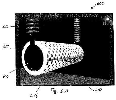
13 [0065] Figure 6A is a schematic three dimensional illustration 600 of a
transparent
14 cylinder 604 having a patterned surface 608. A radiation source (not shown)
is present
within the interior of transparent cylinder 604. The transparent cylinder 604
is suspended
16 above a substrate 610 using a tensioning device 602, which is shown as
springs in
17 illustration 600. One of skill in the art of mechanical engineering will be
familiar with a
18 number of tensioning devices which may be used to obtain the proper amount
of contact
19 between the outer surface 608 of transparent cylinder 604 and the surface
of substrate
610. In one embodiment method of using the apparatus shown in Figure 6A, the
21 apparatus is used to image a radiation-sensitive material (not shown) on a
substrate 610,
22 where substrate 610 is a polymeric film, which may be supplied and
retrieved on a roll to
23 roll system of the kind shown in Figure 2. The transparent cylinder 604 is
lowered toward
24 the polymeric film substrate (or the polymeric film substrate is raised),
until contact is
made with the radiation-sensitive material. The polymeric film, which is
typically
26 elastomeric will create a Van-der-Walls force bond with the radiation-
sensitive material.
27 The transparent cylinder 604 may then be raised (or the polymeric film
substrate lowered)
21
CA 02709718 2010-06-16
WO 2009/094009 PCT/US2008/012901
1 to a position where contact remains between the surface 608 of transparent
cylinder 604
2 and the surface of the radiation-sensitive material, but the tension between
the two
3 surfaces is such that the force placed on the surface 608 is minimal. This
enables the use
4 of very fine nanopatterned features on the surface 608 of transparent
cylinder 604. When
the substrate 610 begins to move, the transparent cylinder 604 will also move,
forcing
6 transparent cylinder 604 to rotate, maintaining the dynamic contact between
the radiation-
7 sensitive material and the underlying polymeric film substrate 610. At any
moment of the
8 dynamic exposure, the contact between the cylinder and a photosensitive
layer is limited
9 to one narrow line. Due to strong Van-der Walls forces between an
elastomeric film, for
example, on the cylinder exterior surface and the radiation sensitive (photo
sensitive)
11 layer on the substrate, contact is maintained uniform throughout the entire
process, and
12 along the entire width of the mask (length) on the cylinder surface. In
instances where
13 Van-der-Walls forces do not provide a strong enough adhesion between the
cylinder
14 contact surface and a photosensitive layer, an actuating (rotating)
cylinder using a stepper-
motor synchronized with the translational movement of the substrate may be
used. This
16 provides a slip-free exposure process for polymeric or other cylinder
surface material
17 which does not provide strong adhesion forces relative to the substrate.
18 [00661 Figure 6B is a schematic of an embodiment 620 where the radiation
used to
19 accomplish imaging is supplied from a radiation source 612 exterior to
cylinder 604, with
the radiation distributed internally 615 and 616 within the hollow portion of
the cylinder
21 604. The radiation may be directed through the transparent cylinder 604
through the
22 patterned mask surface 608 toward the radiation-sensitive surface (not
shown) of
23 substrate 608 using various lenses, mirrors, and combinations thereof.
24 [00671 Figure 6C is a schematic of an embodiment 630 where the radiation
used to
accomplish imaging of the radiation-sensitive material is supplied from a
location which
26 is exterior to the transparent cylinder 604. The exterior radiation source
612 is focused
27 617 into a waveguide 618 and distributed from the waveguide 618 to an
optical grating
22
CA 02709718 2010-06-16
WO 2009/094009 PCT/US2008/012901
1 620 present on the interior surface 601 of the cylinder 604.
2 [0068] Figure 6D is a schematic of an embodiment 640 where the radiation
used to
3 accomplish imaging is supplied from two exterior radiation sources 612A and
612B, and
4 is focused 621 and 619, respectively, upon an optical grating 620 present on
the interior
surface 601 of cylinder 604.
6 [0069] Figure 7A is a schematic 700 showing the use of multiple cylinders,
such as
7 two cylinders 702 and 704, for example, in series to provide multiple
patterning, which
8 may be used to obtain higher resolution, for example. The relative positions
of the
9 cylinders 702 and 704, for example may be controlled using data from an
interferometer
(not shown) in combination with a computerized control system (not shown).
11 [0070] Figure 7B is a cross-sectional schematic 720 showing a pattern 706
created
12 by a first cylinder 702 after imaging and development of a radiation-
sensitive material
13 710. The altered pattern 708 is after imaging and development of the
radiation-sensitive
14 material 710 where the altered pattern 708 is created by use of the first
cylinder 702 in
combination with a second cylinder 704.
16 [0071] Figure 8 shows a cross-sectional schematic of a deformable cylinder
800, the
17 interior 804 of which is pressurized using an apparatus 813 which supplies
an optically
18 transparent gas, such as nitrogen, for example. The outer surface 811 of
deformable
19 cylinder 800 may be a nanopatterned/nanostructured film 812 of a
conformable material,
which can be rolled upon a non-flat substrate 805 so that radiation from
radiation source
21 802 can be precisely applied over a surface 816 of substrate 805.
22 [0072] In another embodiment, a liquid having a refractive index of greater
than one
23 may be used between the cylinder surface and a radiation sensitive (photo
sensitive, for
24 example) material present on the substrate surface. Water may be used, for
example.
This enhances the pattern feature's contrast in the photosensitive layer.
26 [0073] While the invention has been described in detail for a variety of
27 embodiments above, various modifications within the scope and spirit of the
invention
23
CA 02709718 2010-06-16
WO 2009/094009 PCT/US2008/012901
1 will be apparent to those of working skill in this technological field.
Accordingly, the
2 scope of the invention should be measured by the appended claims.
24