Note: Descriptions are shown in the official language in which they were submitted.
CA 02710048 2010-07-16
HIGH EFFICIENCY MICROWAVE AMPLIFIER
BACKGROUND
1. Technical Field
[0001] The present disclosure relates to systems and methods for providing
energy to
biological tissue and, more particularly, to improved apparatus and methods
for amplifying
microwave energy for use during surgical procedures.
2. Background of Related Art
[0002] Energy-based tissue treatment is well known in the art. Various types
of energy (e.g.,
electrical, ultrasonic, microwave, cryogenic, thermal, laser, etc.) are
applied to tissue to achieve a
desired result. Electrosurgery involves application of high radio frequency
electrical current to a
surgical site to cut, ablate, coagulate or seal tissue. In monopolar
electrosurgery, a source or
active electrode delivers radio frequency energy from the electrosurgical
generator to the tissue
and a return electrode carries the current back to the generator. In monopolar
electrosurgery, the
source electrode is typically part of the surgical instrument held by the
surgeon and applied to the
tissue to be treated. A patient return electrode is placed remotely from the
active electrode to
carry the current back to the generator.
[0003] In tissue ablation electrosurgery, the radio frequency energy may be
delivered to
targeted tissue by an antenna or probe. In this instance, a high radio
frequency electrical current
in a microwave range of about 900 MHz to about 5 GHz is applied to a targeted
tissue site to
create an ablation volume, which may have a particular size and shape.
Typically, microwave
apparatus for use in ablation procedures include a microwave generator, which
functions as an
energy source, and a microwave surgical instrument having an antenna assembly
for directing
1
CA 02710048 2010-07-16
the energy to the target tissue. The microwave generator and surgical
instrument are typically
operatively coupled by a cable assembly having a plurality of conductors for
transmitting
microwave energy from the generator to the instrument, and for communicating
control,
feedback and identification signals between the instrument and the generator.
[0004] The microwave generator commonly includes a microwave oscillator
coupled to a
power amplifier. The microwave oscillator generates a relatively low-power
surgical signal that
is amplified by a microwave amplifier to produce a signal of sufficient power
to achieve the
desired effect, e.g., tissue ablation. A user, typically a surgeon, may
specify a particular output
level, which may be accomplished by varying the amplitude of the relatively
low-power input
surgical signal to the microwave amplifier. With decreasing input levels, an
amplifier operates
in linear mode where efficiency decreases, e.g., thermal power dissipation
increases.
Conversely, with increasing input levels, an amplifier operates at or near
saturation mode where
maximum efficiency is achieved and thermal power dissipation is at a minimum.
[0005] Commonly used microwave power amplifiers are known to be inefficient.
For
example, a class AB microwave power amplifier typically exhibits an efficiency
of about 35%.
That is, to achieve a surgical signal of 250W, a class AB power amplifier
requires about 714W
of power, of which 464W is dissipated as thermal energy. The resulting heat
becomes difficult
to manage and may require the use of bulky and costly cooling systems, e.g.,
fans and heat sinks.
Additionally, the excess heat may cause thermal stress to other components of
the generator,
shortening generator life, decreasing reliability, and increasing maintenance
costs.
[0006] Additionally, a class AB amplifier may exhibit crossover distortion
that introduces
undesirable harmonics into the surgical signal, which are known to cause
radiofrequency
interference in excess of acceptable limits.
2
CA 02710048 2010-07-16
SUMMARY
[00071 The present disclosure provides a method and apparatus for an improved
microwave
ablation amplifier having a push-pull configuration which exhibits improved
efficiency over a
wide range of power output levels. A generator in accordance with the present
disclosure may
also exhibit reduced harmonics in the high-power surgical output signal, which
reduces
undesirable radiofrequency interference. In accordance with the present
disclosure, a low power
input signal is maintained at a constant, relatively high level, while the
output level of the
amplifier is adjusted, at least partially, by varying the supply voltage
(e.g., the "rail" voltage) of
a push-pull class B amplifier output stage. At least one LDMOS (laterally
diffused metal oxide
semiconductor) transistor, such as without limitation, a BLC6GIOLS-160,
manufactured by NXP
Semiconductors of Eindhoven, The Netherlands, may be included in the amplifier
output stage.
[00081 Also presented is a method and apparatus for controlling the disclosed
microwave
generator. A disclosed amplifier control unit is in operable communication
with at least one
sensor configured to receive a sensor signal indicative of one or more
operating condition of the
generator and/or amplifier circuit. The amplifier control unit is operably
coupled to a rail voltage
control unit and a drive control unit. The rail voltage control unit is
configured to receive a rail
voltage control signal and in response thereto provide a rail control voltage
in accordance
therewith to an amplifier output stage. The drive control unit is configured
to receive a drive
control signal and in response thereto provide a drive signal in accordance
therewith to an input
of the amplifier output stage. The drive control unit may also include an
input to receive a
relatively low power microwave signal. Additionally or alternatively, a signal
source may be
included within the drive control unit.
3
CA 02710048 2010-07-16
[0009] The amplifier control unit, in response to an at least one sensor
signal, dynamically
varies an operating parameter, e.g., a rail voltage and/or an input level, to
achieve efficient and
stable operation of the generator over a range of output power levels. The
control unit may
impose a rail voltage minima on the presently disclosed amplifier. For
example, the rail voltage
may be held to greater than about 14V in order to avoid undesirable increases
in the internal
capacitance of an LDMOS device, such as without limitation a BLC6G10LS-160 UHF
power
LDMOS transistor manufactured by NXP B.V. of The Netherlands, which may cause
the
amplifier to detune and/or become unstable. The minimum rail voltage is
dependent upon the
LDMOS utilized in an embodiment, and embodiments utilizing LDMOS devices other
than a
BLC6GIOLS-160 may require a minimum rail voltage that is greater than, or less
than, about
14V. In another example, at a lower portion of the amplifier's operating
power, the controller
may be configured to increase power output by first causing the drive
attenuation control unit to
output a signal of sufficient amplitude to cause the LDMOS device(s) to
operate outside the
linear operating region thereof, thereby achieving improved operating
efficiency. When the
LDMOS devices are operating outside the linear region, output power may be
further increased
by increasing the rail voltage. The drive signal may be correlated to the rail
voltage, e.g., the
drive signal may be increased proportionally to the rail voltage.
[0010] The controller may include a processor having the capability of
executing a set of
programmed instructions for executing a method of controlling a microwave
ablation generator
as disclosed herein.
[0011] In an embodiment, the disclosed electromagnetic signal amplifier
includes a gain
stage electrically disposed between a supply rail and a return rail. The gain
stage includes an
input and an output. A rail voltage controller is coupled to the supply rail
and/or the return rail,
4
CA 02710048 2010-07-16
wherein the rail voltage controller includes is configured to provide a rail
voltage responsive to a
rail voltage control signal. A drive controller is coupled to the gain stage
input and provide an
input signal to the gain stage in response to a drive control signal. The
disclosed electromagnetic
signal amplifier includes a sensor configured to sense an operational
parameter of the amplifier,
such as an output voltage, and to provide a corresponding sensor signal to an
amplifier
controller. The amplifier controller is configured to provide a rail voltage
control signal to the
rail voltage controller, and a drive control signal to the drive controller.
[0012] The present disclosure is also directed to a method for controlling a
microwave
amplifier that includes setting a rail voltage to a minimum value and a drive
signal to a minimum
amplitude. The resultant output signal level is measured and compared to a
desired output signal
level. The desired output signal level may be determined by the user. If the
output signal is not
equal (or not substantially equal to) the desired output level, the value of
the drive signal is
examined. If the drive signal is not at a maximum value, the drive signal is
increased. If the
drive signal equals (or substantially equals) a maximum value, the rail
voltage is increased.
[0013] Also disclosed is a method of controlling a microwave amplifier that
includes setting
a rail voltage to an initial value, which may be a minimum value. A rail
current is measured and
compared to a target criteria, e.g., O.IA. If the rail current does not meet
(e.g., not equal to or
substantially not equal to) the target criteria, the bias voltage is
increased. If the rail current
meets (e.g., equal to or substantially equal to) the target criteria, the bias
voltage value is stored,
and the rail voltage is increased. If the rail voltage does not meet the
target criteria, then the bias
voltage is adjusted accordingly until the target voltage is met. The rail
current is again measured
and the process iterates until the rail voltage is at a maximum value.
CA 02710048 2010-07-16
BRIEF DESCRIPTION OF THE DRAWINGS
[0014] The above and other aspects, features, and advantages of the present
disclosure will
become more apparent in light of the following detailed description when taken
in conjunction
with the accompanying drawings in which:
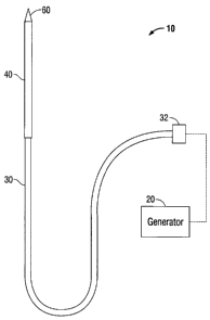
[0015] Fig. 1 shows a diagram of a microwave ablation system having an
electromagnetic
surgical ablation probe in accordance with the present disclosure;
[0016] Fig. 2 is a block diagram of an amplifier having rail voltage and drive
attenuation
control in accordance with the present disclosure;
[0017] Fig. 3 is a flow diagram of a method of controlling rail voltage and
drive attenuation
of an amplifier in accordance with the present disclosure;
[0018] Fig. 4 shows a block diagram of an amplifier having rail voltage and
bias control in
accordance with the present disclosure;
[0019] Fig. 5 is a flow diagram of a method of controlling rail voltage and
bias voltage of an
amplifier in accordance with the present disclosure;
[0020] Fig. 6 is a graph illustrating a relationship between rail current and
rail voltage in
accordance with the present disclosure;
[0021] Fig. 7 is a graph illustrating a relationship between capacitance and
drain-to-source
voltage in accordance with the present disclosure;
[0022] Fig. 8 is a circuit diagram illustrating actual and equivalent
inductive and capacitive
elements of a gain stage of an amplifier in accordance with the present
disclosure;
[0023] Fig. 9A is a graph illustrating the harmonic power distribution of a
prior-art amplifier;
6
CA 02710048 2010-07-16
[0024] Fig. 9B is a graph illustrating the harmonic power distribution of an
amplifier in
accordance with the present disclosure;
[0025] Fig. 1OA is a graph illustrating a relationship between output power
and efficiency of
a prior-art amplifier;
[0026] Fig. I OB is a graph illustrating a relationship between output power
and efficiency of
an amplifier in accordance with the present disclosure;
[0027] Fig. 11 A is a graph illustrating the harmonic power distribution of a
prior-art
amplifier operating at about half-power; and
[0028] Fig. 11 B is a graph illustrating the harmonic power distribution of an
amplifier in
accordance with the present disclosure operating at about half-power.
DETAILED DESCRIPTION
[0029] Particular embodiments of the present disclosure are described
hereinbelow with
reference to the accompanying drawings; however, it is to be understood that
the disclosed
embodiments are merely exemplary of the disclosure, which may be embodied in
various forms.
Well-known functions or constructions are not described in detail to avoid
obscuring the present
disclosure in unnecessary detail. Therefore, specific structural and
functional details disclosed
herein are not to be interpreted as limiting, but merely as a basis for the
claims and as a
representative basis for teaching one skilled in the art to variously employ
the present disclosure
in virtually any appropriately detailed structure.
[0030] Fig. 1 shows an embodiment of a microwave ablation system 10 in
accordance with
the present disclosure. The microwave ablation system 10 includes an
electromagnetic surgical
ablation probe 40 connected by a cable 30 to a connector 32, which may further
operably
7
CA 02710048 2010-07-16
connect the probe 40 to a generator assembly 20. Generator assembly 20 may
include a source
of ablation energy, e.g., microwave or RF energy in the range of about 500 MHz
to about 5 GHz.
[00311 With reference to Fig. 2, a block diagram of a push-pull amplifier 100
having a push-
pull output stage 140 is presented. Output stage 140 may be configured as a
class B push-pull
output stage having a complementary pair of transistors 142, 144. Transistor
142 may be an
NPN transistor that is configured to supply current from supply rail 125 to an
output load, e.g., a
microwave ablation probe 105. Transistor 144 may be a PNP transistor that is
configured to sink
current from the output load to a ground rail 126. Ground rail 126 may be
alternatively be
configured as a negative supply rail.
[00321 Amplifier 100 includes amplifier controller 110 that is configured to
receive at least
one sensor signal and in response thereto output at least one corresponding
control signal to at
least one of a rail voltage controller 120 and a drive controller 130.
Amplifier controller 110 is
operably coupled to at least one sensor 150 that is adapted to sense an
electrical property of an
output signal, e.g., voltage, current, impedance. Additionally or
alternatively, sensor 150 may
sense an instantaneous, peak, RMS, or moving average property of an output
signal. Amplifier
controller 110 may be configured to perform a method of controlling a push
pull amplifier 100 as
will be described in further detail hereinbelow.
[0033] Rail voltage controller 120 is configured to provide a variable output
voltage to
supply rail 125 in response to a rail voltage control signal (not explicitly
shown) received from
amplifier controller 110. The rail voltage control signal may be any suitable
signal, e.g., an
analog or digital signal. Rail voltage controller 120 may include a power
supply having a fixed
or variable output voltage. It is envisioned that rail voltage controller 120
may encompass any
suitable manner of voltage regulation, such as, and without limitation, an
LM317 voltage
8
CA 02710048 2010-07-16
regulator integrated circuit manufactured by National Semiconductor Corp. of
Santa Clara,
California, US. In an embodiment supply rail 125 is referenced to ground at
return rail 126. Rail
voltage controller 120 may be configured to provide a bipolar supply wherein
e.g., a positive
voltage is provided by rail voltage controller 120 to supply rail 125 and a
negative voltage is
provided by rail voltage controller 120 to return rail 126.
[00341 Drive controller 130 is configured to provide an input signal to the
output stage 140.
Drive controller 130 may include an oscillator 134 configured to generate a
radiofrequency
ablation signal that is operable coupled to an output thereof to an
attenuation network 136. In an
embodiment, drive controller 130 may include an RF signal input (not
explicitly shown) that is
operably coupled to an oscillator. Drive controller 130 includes a drive
control input that is
adapted to receive a drive control signal from amplifier controller 110.
Attenuation network 136
is responsive to the drive control signal, whereby the drive control signal
defines the degree of
attenuation provided by attenuation network 136. Drive controller 130 may
provide signal
attenuation by any suitable manner of attenuation, for example, and without
limitation, voltage-
controlled amplifier (e.g., a unity gain voltage controlled amplifier), a
digital potentiometer, or a
digitally-switched voltage dividing network
[00351 Turning to Fig. 3, a rail voltage control method 200 for operating push-
pull amplifier
100 shows initial step 210 which is an entry point wherein initialization may
be performed. In
the step 215, the rail voltage and drive level are set to a minimum. In an
embodiment, amplifier
controller 110 causes rail voltage controller 120 to output a minimum voltage,
which may be in a
range of about OV to about 30V, e.g., 14V, and amplifier controller 110 may
additionally or
alternatively cause drive controller 130 to be set to a minimum drive level
(i.e., maximum drive
attenuation.) In the step 220, a desired output level is set, e.g., wherein a
user selects a desired
9
CA 02710048 2010-07-16
output level, which may be, for example and without limitation, an output
voltage, output
current, or other signal property. In the step 225, a main operational loop is
entered wherein an
output level is measured. For example, amplifier controller 110 may poll an
input thereof
corresponding to an output of sensor 150. Sensor 150 may provide a signal to
amplifier
controller 110 in analog format, or in digital format. In one embodiment, the
step 225 may
include an analog-to-digital conversion of the sensed output.
[00361 In the step 230, the measured level is compared to the desired level to
determine
whether the output level equals the desired level. It is to be understood that
comparisons
performed by the methods disclosed herein may include a tolerance within which
the values
being compared are evaluated, e.g., quantities may be within a range and/or
substantially equal to
be deemed equal. If a positive determination is made (e.g., output level is
acceptably equal to
the desired level as described herein) the process iterates to the step 225.
[00371 If a negative determination is made, that is, the output level does not
equal the desired
level, the step 235 is performed wherein a determination is made whether the
drive level is set to
a maximum value (or alternatively, within a tolerance range of, or
substantially equal to, a
maximum value.) If it is determined the drive level is set to a maximum value
(i.e., minimum
drive attenuation), the step 245 is performed wherein the rail voltage is
increased. For example,
amplifier controller 110 causes rail voltage controller 120 to increase the
output voltage thereof.
The output voltage may be increased by a predetermined amount. Subsequent to
step 245, the
process iterates to step 225. Conversely, if it is determined the drive level
is not set to a
maximum value, the step 240 is performed wherein the drive level is increased
(i.e., drive
attenuation is reduced). Subsequent to step 240, the process iterates to the
step 225. In an
embodiment, step 240 or step 245 includes a time delay.
CA 02710048 2010-07-16
[0038] With reference now to Fig. 4, an amplifier stage 300 according to the
present
disclosure includes a gain element 330, which may be a field effect transistor
(FET), a gallium
nitride (GaN) high electron mobility transistor (HEMTs), gallium arsenide
(GaAs) FET, or a
laterally diffused metal oxide semiconductor transistor (LDMOS), such as
without limitation, a
BLC6G10LS-160 as described hereinabove. Unless stated otherwise, in the
following
description is it to be understood that gain element 330 is an N channel
device, such as a
BLC6G10LS-160. Gain element 330 may alternatively be a P-channel device. Gate
331 of gain
element 330 may be slightly biased at about O.IA of the rail current. However,
as seen in Fig. 6
rail current will increase as rail voltage is increased. To address this,
amplifier stage 300
includes a current sensor 310 that is adapted to measure a bias current of
gain element 330 and
communicate a value corresponding thereto to amplifier controller 110'.
Amplifier 300 includes
bias controller 320 that is in operable communication with amplifier
controller 110'. Bias
controller 320 is responsive to a bias control signal received from amplifier
controller 110' to
provide a bias current to gain element 330 in accordance with a method
described below.
[0039] As shown in Fig. 5, a biasing method 400 for biasing a gain stage 300
begins at step
410 which is an entry point wherein initialization may be performed. In step
415, the rail voltage
is set to an initial value, which may be a minimum value, e.g., 14V. In step
420, the rail current
is measured and compared to a target current, e.g., 0.1A, to determine whether
the rail current
equals the target rail current. If the measured current does not equal the
target current, step 425
is performed wherein the bias voltage is increased. In an embodiment, the bias
voltage is
increased by a fixed amount. Steps 420 and 425 are repeated iteratively until
the rail current
equals the target current.
11
CA 02710048 2010-07-16
[0040] If the measured rail current equals the target current, step 430 is
performed wherein
the bias voltage is stored. Step 435 is then performed wherein the rail
voltage is increased. A
comparison is performed in step 440 to determine whether the rail voltage
equals a maximum
voltage. If the rail voltage equals a maximum voltage, the bias adjustment is
complete and the
process concludes in step 465.
[0041] If, however, the rail voltage does not equal a maximum voltage, step
445 is
performed wherein it is determined whether the rail current equals a target
current value, e.g.,
O.IA. If the rail current is determined to equal the target current, the
process iterates at step 430
wherein the bias voltage is stored and the process continues as described
herein. If the rail
current does not equal the target current value, the rail current is tested in
the step 450 to
determine whether the rail current is less than the target current value. If
it is determined the rail
current is less than the target current value, the step 455 is performed
wherein the bias voltage is
increased, whereupon the process iterates to step 445. Conversely, if it is
determined the rail
current is not less than (e.g., greater than) the target current value, the
step 460 is performed
wherein the bias voltage is decreased, whereupon the process iterates to step
445.
[0042] In embodiments wherein the gain element 330 is P-channel device, the
bias voltage is
adjusted in an opposite manner, e.g., decreased in the step 455 and/or
increased in the step 460,
in accordance with the characteristics of a P-channel device.
[0043] Fig. 7 illustrates a relationship between internal capacitances Ciss,
Coss, and Crss
exhibited by a gain element, e.g., a FET, and a drain-to-source voltage VDS,
e.g., a rail voltage.
As can be seen, as VDS decreases, the internal capacitances Cass, Coss, and
Crss of the FET
increase. The capacitance increases exponentially as VDS approaches zero. In a
tuned gain stage
700 such as illustrated in Fig. 8, reducing VDS, e.g., the rail voltage, lower
than about 14V would
12
CA 02710048 2010-07-16
result in a significant detuning of gain stage 700, which may result in
decreased efficiency and
instability. Accordingly, the present disclosure contemplates a minimum rail
voltage of about
14V.
[0044] A comparison between a prior art amplifier, and an amplifier in
accordance with the
present disclosure, is shown in Fig. 9A which illustrates a graph of the power
spectrum of a prior
art single stage (class B) amplifier operating at 915 MHz at full power of
about +52.55 dBm. As
can be seen, a +9.341 dBm second harmonic is present at 1.83 GHz and a third
harmonic of
-12.63 dBm is present at 2.745 GHz. Fig. 9B illustrates an amplifier according
to the present
disclosure operating on a similar 915 MHz input signal as the Fig. 9A example.
At full power of
about +52.67dBm, which for illustration purposes only is effectively the same
as the prior art
example (i.e., within. 12 dBm of the prior art example), the Fig. 9B spectrum
of the presently
disclosed amplifier exhibits a second harmonic of 5.339 dBm, and a third
harmonic of -27.32
dBm. This represents an improvement over the prior art of about a 4 dBm
reduction in second-
order harmonics and of about a 14.7 dBm reduction in third-order harmonics.
[0045] A comparison of harmonic performance at about half-power is illustrated
with
reference to Figs. 11 A and 11 B, which correspond to a prior art amplifier
and an amplifier in
accordance with the present disclosure, respectively. As can be seen, the
present amplifier
exhibits an improvement of about a 3 dBm reduction in second-order harmonics.
Third-order
harmonics, however, increase about 12 dBm in the present amplifier.
[0046] Continuing the comparison, Fig. 1 OA is a graph representing a
relationship between
output power and efficiency to increasing input power level of a prior art
amplifier, while Fig.
I OB represents a relationship between output power and efficiency to
increasing rail voltage of
an amplifier according to the present invention. As will be readily
appreciated, an amplifier
13
CA 02710048 2010-07-16
according to the present invention exhibits a much higher and flatter
efficiency curve than that of
the prior art amplifier. For example, and with reference to Fig. 1 OA, a prior
art amplifier at about
50% output power exhibits an efficiency of about 40%. In contrast, and with
reference to Fig.
I OB, an amplifier in accordance with the present disclosure at about 50%
output power exhibits
an efficiency of out 70%. As can be seen, the prior art amplifier has an
efficiency which can be
as low as 15%, while the efficiency of the presently disclosed amplifier never
drops below 68%
over an entire operating range thereof.
[0047] While several embodiments of the disclosure have been shown in the
drawings and/or
discussed herein, it is not intended that the disclosure be limited thereto,
as it is intended that the
disclosure be as broad in scope as the art will allow and that the
specification be read likewise.
Therefore, the above description should not be construed as limiting, but
merely as
exemplifications of particular embodiments. The claims can encompass
embodiments in
hardware, software, or a combination thereof. Those skilled in the art will
envision other
modifications within the scope and spirit of the claims appended hereto.
14