Note: Descriptions are shown in the official language in which they were submitted.
CA 02710147 2012-02-13
1
A Voltage Source Converter and a method for
control thereof
The present invention relates to a Voltage Source Converter (VSC)
for converting direct voltage into alternating voltage and conversely,
and a method for controlling the VSC.
The converter to be controlled may have any number of said
phase legs, but it has normally three such phase legs for having
a three phase alternating voltage on the alternating voltage side
thereof.
A Voltage Source Converter of this type may be used in all kinds
of situations, in which direct voltage is to be converted into
alternating .voltage or conversely, in which examples of such
uses are in stations of HVDC-plants (High Voltage Direct Cur-
rent), in which direct voltage is normally converted into a three-
CA 02710147 2010-06-17
WO 2009/092435 PCT/EP2008/050612
2
phase alternating voltage or conversely, or in so-called back-to-
back-stations in which alternating voltage is firstly converted
into direct voltage and this is then converted into alternating
voltage, as well as in SVCs (Static Var Compensator), in which
the direct voltage side consists of one or more capacitors hang-
ing freely. However, the present invention is not restricted to
these applications, but other applications are also conceivable,
such as in different types of drive systems for machines, vehi-
cles etc.
Such a Voltage Source Converter may have more than two cur-
rent valves per phase leg and then deliver pulses of more than
two different amplitudes or levels on said phase output, such as
in a NPC-type converter (Neutral Point Clamped). Each such
valve may also have a plurality of said power semiconductor
devices of turn-off type connected in series for being able to
together block the voltage to be blocked in the blocking state of
the valve. IGBTs (Insulated Gate Bipolar Transistor) are
normally used in such converters as semiconductor devices of
turn-off type, but any such semiconductor device, such as
IGCTs (Integrated Gate Commutated Thyristor) is within the
scope of the present invention.
A two level converter of this type is very schematically shown in
appended Fig 1 for illuminating the present invention but not in
any way restrict it thereto. This VSC converter 1 has three
phase legs 2, 3, 4 with two current valves 5-10 each, each con-
sisting of at least one semiconductor device of turn-off type,
such as an IGBT 11, and a rectifying member in the form of a
diode 12 connected in anti-parallel therewith. A mid point of
each phase leg forms a phase output 13, 14, 15 for connection
through phase reactors 16, 17, 18 to a three-phase alternating
voltage network 19. Opposite ends of each phase leg is con-
nected to opposite poles 20, 21 on a direct voltage side of the
converter, such as a positive and negative pole conductor of a
direct voltage network 22.
CA 02710147 2010-06-17
WO 2009/092435 PCT/EP2008/050612
3
The converter has an arrangement 23 configured to control the
semiconductor devices 11 of the valves to generate a train of
pulses with determined amplitudes according to a Pulse Width
Modulation (PWM) pattern on the respective phase output for
creating an alternating voltage on the respective line of the al-
ternating voltage network 19. When for example the semicon-
ductor device of the valve 7 is turned on a positive pulse will
result on the phase output 15, and if instead the semiconductor
device of the valve 10 is turned on a negative pulse with the
same amplitude will result on the phase output 15. During the
positive half cycle of the alternating voltage to be generated on
the phase output 15 the semiconductor device of the valve 7 will
alternatively be turned on and off for generating a train of posi-
tive pulses, and during the negative half cycle of said alternating
voltage the semiconductor device of the valve 10 will be alter-
natively turned on and off. The pulse number, i.e. the number of
pulses resulting from this Pulse Width Modulation during a pe-
riod of an alternating voltage obtained by this control, may typi-
cally be as high as 15-25 for obtaining an attractive shape of the
curve on the alternating voltage side while keeping costs of
filtering equipment at an acceptable level.
Not neglectible losses are created in the semiconductor devices
of the valves. These losses are of two types, namely conduction
losses resulting in the conducting state of the semiconductor
device and switching losses resulting when the semiconductor
device is turned on or turned off. The problem of high switching
losses is of course the more important the higher the switching
frequency, i.e. said pulse number. Semiconductor devices with a
voltage blocking capacity rating of a low level have considerably
lower switching losses than such semiconductor devices with
such a rating of a higher level, so that a higher number of such
semiconductor devices with a voltage blocking capacity rating of
a lower level may be connected in series instead of one or few
such semiconductor devices with a rating of a higher level for by
that considerably reducing the switching losses of the valve in
CA 02710147 2012-02-13
4
question. However, this will then result in higher conduction
losses of the valve, since a semiconductor device having a volt-
age blocking capacity rating of a higher level will have consid-
erably lower conduction losses. It may be mentioned as an ex-
ample that for a pulse number of 23 the switching losses of five
1200 V IGBTs connected in series would be 1300 u compared to
12000 u for a 6500 V IGBT, whereas the conduction losses
would for said series connection be 8000 u and for said single
6500 V IGBT 3200 u. Accordingly, there is for each application
intended for such a VSC converter a trade off between
conduction losses and switching losses when determining the
number of such semiconductor devices of turn-off type to be
connected in series in each said valve of the converter.
SUMMARY OF THE INVENTION
An object of the present invention is to provide a converter of
the type defined in the introduction addressing the problems
mentioned above with respect to losses created in the valves of
the converter for making it possible to reduce the total losses
created in such valves with respect to such converters already
known.
More specifically, the present invention provides a system
comprising a valve in a Voltage Source Converter and a control
arrangement,
wherein said valve comprises one first semiconductor device
of turn-off type with a voltage blocking capacity rating of a first, high
level and connected in parallel with a series connection of a plurality
of second semiconductor devices of turn-off type with a voltage
blocking capacity rating of a second, lower level, wherein said control
arrangement is configured to switch said valve into a conducting
state starting from a forward biased blocking state of the valve by
controlling said second semiconductor devices to be turned on and
then said first semiconductor devices to be turned on with a delay
sufficient for the voltage across said valve to fall to a fraction of less
than 10% of the voltage across the valve in said forward biased
blocking state of the valve and the end of the conducting state to turn
off said first semiconductor device in advance of turning said second
semiconductor devices off, and wherein said second semiconductor
devices are turned off by said control arrangement after a majority of
CA 02710147 2014-11-20
4a
recombinations of charge carriers in said first semiconductor device
has taken place.
The present invention also provides a Voltage Source Converter, for
converting direct voltage into alternating voltage and conversely, has
at least one phase leg configured to be connected to opposite poles
on a direct voltage side of the converter and comprises:
a series connection of at least two current valves, each valve
having the features of a valve as described herein, where
a mid point of said series connection of valves forms a phase
output which is configured to be connected to an alternating voltage
side of the converter,
the converter further comprising a control arrangement
configured to control the semiconductor devices of said valves to
generate a train of pulses with determined amplitudes according to a
Pulse Width Modulation (PWM) pattern on said phase output, where
the control arrangement comprises a control arrangement as
described herein.
According to an aspect of the present invention, there is provided a
system comprising:
a valve in a Voltage Source Converter (VSC); and
a control arrangement,
wherein said valve comprises one first semiconductor device
of turn-off type with a voltage blocking capacity rating of a first, high
level and series-connected second semiconductor devices of turn-off
type with a voltage blocking capacity rating of a second, lower level,
the first semiconductor device is connected in parallel with the
series-connected second semiconductor devices, and said control
arrangement is configured to switch said valve into a conducting
state starting from a forward biased blocking state of the valve by
controlling said second semiconductor devices to be turned on and
then said first semiconductor device to be turned on with a delay
sufficient for the voltage across said valve to fall to a fraction of less
than 10% of the voltage across the valve in said forward biased
blocking state of the valve and at the end of the conducting state to
turn off said first semiconductor device in advance of turning said
second semiconductor devices off, where said second
semiconductor devices are turned off by said control arrangement
after a majority of recombinations of charge carriers in said first
semiconductor device has taken place.
CA 02710147 2014-11-20
4b
According to another aspect of the present invention, there is
provided a Voltage Source Converter (VSC) for converting direct
voltage into alternating voltage and conversely, which has at least
one phase leg configured to be connected to opposite poles on a
direct voltage side of the converter and comprising:
a series connection of at least two current valves, each of said
valves comprising one first semiconductor device of turn-off type with
a voltage blocking capacity rating of a first, high level and series-
connected second semiconductor devices of turn-off type with a
voltage blocking capacity rating of a second, lower level, the first
semiconductor device being connected in parallel with the series-
connected second semiconductor devices, wherein
a mid point of said series connection of valves forms a phase
output which is configured to be connected to an alternating voltage
side of the converter,
the converter further comprising a control arrangement
configured to control the semiconductor devices of said valves to
generate a train of pulses with determined amplitudes according to a
Pulse Width Modulation (PWM) pattern on said phase output, where
the control arrangement and said control arrangement is configured
to switch said valve into a conducting state starting from a forward
biased blocking state of the valve by controlling said second
semiconductor devices to be turned on and then said first
semiconductor device to be turned on with a delay sufficient for the
voltage across said valve to fall to a fraction of less than 10% of the
voltage across the valve in said forward biased blocking state of the
valve and at the end of the conducting state to turn off said first
semiconductor device in advance of turning said second
semiconductor devices off, where said second semiconductor
devices are turned off by said control arrangement after a majority of
recombinations of charge carriers in said first semiconductor device
has taken place.
According to another aspect of the present invention, there is
provided a method for controlling a Voltage Source Converter (VSC)
comprising a series connection of at least two current valves, said
valves comprising at least one semiconductor device of turn-off type
and one rectifying member connected in anti-parallel therewith,
wherein the method is carried out for a converter in which each said
valve comprises one first semiconductor device of turn-off type with a
CA 02710147 2014-11-20
4c
voltage blocking capacity rating of a first, high level and series-
connected second semiconductor devices of turn-off type with a
voltage blocking capacity rating of a second, lower level, the first
semiconductor device being connected in parallel with the series-
connected second semiconductor devices, that said valve is
switched into a conducting state starting from a forward biased
blocking state of the valve by controlling said second semiconductor
devices to be turned on and then said first semiconductor device to
be turned on with a delay sufficient for the voltage across said valve
to fall to a fraction of less than 10% of the voltage across the valve in
said forward biased blocking state of the valve, and that at the end of
the conducting state said first semiconductor device is turned off in
advance of turning said second semiconductor devices off, where
said second semiconductor devices are turned off after a majority of
recombinations of charge carriers in said first semiconductor device
has taken place.
This object is according to the invention obtained by providing a
converter of the type defined in the introduction, which is
characterized in that each said valve comprises one first semi-
conductor device of turn-off type with a voltage blocking capac-
ity rating of a first, high level and connected in parallel therewith
a series connection of a plurality of second semiconductor de-
vices of turn-off type with a voltage blocking capacity rating of a
second, lower level, and that said control arrangement is con-
figured to switch a said valve into a conducting state starting
from a forward biased blocking state of the valve by controlling
said second semiconductor devices to be turned on and then
said first semiconductor device to be turned on with a delay suf-
ficient for the voltage across said valve to fall to a fraction of
CA 02710147 2010-06-17
WO 2009/092435 PCT/EP2008/050612
less than 10% of the voltage across the valve in said forward
biased blocking state of the valve and at the end of the con-
ducting state to turn off said first semiconductor device suffi-
ciently in advance of turning said second semiconductor devices
5 off for enabling a majority of recombinations of charge carriers
in said first semiconductor device to take place before said
turning off of the second semiconductor devices.
Accordingly, said first semiconductor device with a voltage
blocking capacity rating of a high level will be turned on and
turned off when the voltage across the valve is low, so that the
switching losses will be determined by the configuration of said
second semiconductor devices having a voltage blocking capac-
ity rating of a lower level, whereas the current will during the
conducting state of the valve flow through said first semicon-
ductor device, which will then determine the conduction losses
of the valve. This means that the low conduction losses of a
semiconductor device with a voltage blocking capacity rating of
a high level may be combined with the low switching losses of
semiconductor devices with a voltage blocking capacity rating of
a lower level, so that the losses of the valve may be reduced
considerably without sacrificing the good performance of the
converter.
According to an embodiment of the invention the number of said
second semiconductor devices connected in series and in par-
allel with one said first semiconductor device are 3-
10 or 4-
7. These are suitable numbers of such second semiconductor
devices per first semiconductor device, but it is pointed out that
the number of first semiconductor devices may of course be
comparatively high, such as 20, in which case the number of
second semiconductor devices in the valve may well be about
100. The relationship of said first high level/said second low
level is then approximately equal to the number of second semi-
conductor devices connected in parallel with said first semicon-
CA 02710147 2010-06-17
WO 2009/092435 PCT/EP2008/050612
6
ductor device for fully utilize the properties of each such semi-
conductor device, also with respect to the costs thereof.
According to another embodiment of the invention said control
arrangement is configured to control said valves to deliver a
said Pulse Width Modulation pattern with a pulse number p 10,
13-40 or 15-25, in which the pulse number is defined as the
number of pulses resulting from said Pulse Width Modulation
pattern during a period of an alternating voltage obtained by
said control on said phase output. The invention is particularly
interesting when the pulse number p is comparatively high, so
that the switching losses of a semiconductor device with a volt-
age blocking capacity rating of a high level will be considerable
with respect to the conduction losses of such a semiconductor
device.
According to another embodiment of the invention said delay is
less than 10% of an average duration of a conducting state of
said valve, which means that the current may be converted to
flow through said first semiconductor device during the major
part of said conducting state. This delay will for a specific con-
verter be a fixed delay, which typically may be in the order of
Ps.
According to another embodiment of the invention said turning-
off in advance is controlled to take place at a time being suffi-
cient for reducing the current through said first semiconductor
device to be less than 10% of the current therethrough in the
conducting state of said valve, which means that the valve may
be transferred to the forward biased blocking state when sub-
stantially all the current flows through said second semiconduc-
tor devices, which will then determine the switching losses cre-
ated. The control arrangement is preferably configured to control
said second semiconductor device of the valve to turn on and
turn off when a saw tooth voltage used for said PWM crosses a
reference alternating voltage, and to control the first semicon-
CA 02710147 2010-06-17
WO 2009/092435 PCT/EP2008/050612
7
ductor device at times being with a certain delay or prior to the
control of the second semiconductor devices.
According to other embodiments of the invention said first and
second semiconductor devices are IGBTs (Insulated Gate Bipo-
lar Transistor) and IGCTs (Integrated Gate Commutated Thyris-
tor), respectively.
According to another embodiment of the invention said first
semiconductor device has a said first, high level 3kV, ?.. 5kV, ?_
10kV or 5kV-30kV. These are suitable levels for the voltage
blocking capacity rating of said first semiconductor device, in
which the corresponding level will for the second semiconductor
devices typically be 1/3-1/7 thereof.
According to another embodiment of the invention each said
valve comprises a series connection of a plurality of units having
on one hand one first semiconductor device and on the other a
series connection of second semiconductor devices connected
in parallel therewith, and said control arrangement is configured
to control all said first semiconductor devices of the valve sub-
stantially simultaneously and all second semiconductor devices
of the valve substantially simultaneously.
According to another embodiment of the invention said number
of first semiconductor devices in said valve adapted to be con-
trolled simultaneously 3, 5, 10,
20, 20-130 or 40-80. The
higher numbers are typically to be used for the application of a
converter according to the invention in HVDC-plants in which
voltages to be handled may well be in the order of 400 kV ¨ 800
kV.
According to another embodiment of the invention said control
arrangement is configured to control said valves to generate an
alternating voltage on said phase output having a frequency of
Hz ¨ 70 Hz, 50 Hz or 60 Hz. These are suitable frequencies
CA 02710147 2010-06-17
WO 2009/092435 PCT/EP2008/050612
8
for an alternating voltage to be generated on said phase output
of the converter.
According to another embodiment of the invention said valve
has a first rectifying member with a voltage blocking capacity
rating of a third, high level connected in anti-parallel with said
first semiconductor device and a plurality of second rectifying
members with a voltage blocking capacity rating of a fourth,
lower level connected in series and in anti-parallel with said
series connection of second semiconductor devices, which is
suitable for a good function of each said valve and the con-
verter, and according to a further development of this embodi-
ment said valve comprises a third semiconductor device of turn-
off type connected in series with said first rectifying member and
in parallel with said first semiconductor device, and said control
arrangement is configured, when said valve is in a state in which
the current flows through the rectifying members thereof, to
control said third semiconductor device to turn off prior to a
main commutation of the current to flow through a valve on the
other side of said mid point than said valve for having the cur-
rent commutated into the second rectifying members before
such a main commutation. This means that the losses created in
said valve may be reduced even more, since said first rectifying
member will have a lower on-state voltage than the on-state
voltage of the series connection of said second rectifying
members, so that the current will go through the first rectifying
member when it flows through the rectifying members of such a
valve, but this means that would then a said main commutation
take place comparatively high losses would result in this first
rectifying member. By commutating the current into the second
rectifying members before a said main commutation of the
current to flow through the valve on the other side of said mid
point the losses will be determined by the properties of said
second rectifying members and by that be considerably lower.
CA 02710147 2012-02-13
9
According to another embodiment of the invention said third
semiconductor device is a MOS transistor. This is advanta-
geous, since such a transistor can have an on-state voltage be-
ing neglectible at rated current with respect to the forward volt-
age drop of a said first rectifying member with a voltage blocking
capacity rating of a high level, so that this third semiconductor
device will only contribute marginally to the on-state losses of
the converter.
According to another embodiment of the invention the number of
said second rectifying members is the same as the number of
said second semiconductor devices, and one said second recti-
fying member is connected in anti-parallel with each said semi-
conductor device. Said rectifying members are preferably recti-
fying diodes.
According to another embodiment of the invention the converter
is configured to have said direct voltage side connected to a di-
rect voltage network for transmitting High Voltage Direct Current
(HVDC) and the alternating voltage side connected to an alter-
nating voltage phase line belonging to an alternating voltage
network.
According to a further embodiment of the invention said
converter is a part of a SVC (Static Var Compensator) with the
direct voltage side formed by capacitors hanging freely and the
alternating voltage phase output connected to an alternating
voltage network.
According to another embodiment of the invention the converter
is configured to have a direct voltage across said two poles be-
ing 1 kV ¨ 1200 kV, 10 kV ¨ 1200 kV or 100 kV ¨ 1200 kV.
CA 02710147 2012-02-13
=
The present invention also provides a method for controlling a Voltage
Source Converter (VSC) comprising a series connection of at least two
current valves, said valves comprising at least one semiconductor device
of turn-off type and one rectifying member connected in anti-parallel
5 therewith,
wherein each valve comprises one first semiconductor device of
turn-off type with a voltage blocking capacity rating of a first, high level
and
is connected in parallel with a series connection of a plurality of second
semiconductor devices of turn-off type with a voltage blocking capacity
10 rating of a second, lower level, the method comprising:
switching said valve into a conducting state starting from a forward
biased blocking state of the valve by controlling said second
semiconductor devices to be turned on and controlling said first
semiconductor devices to be turned on with a delay sufficient for the
voltage across said valve to fall to a fraction of less than 10% of the
voltage across the valve in said forward biased blocking state of the valve;
and
turning off said first semiconductor device at the end of the
conducting state in advance of turning said semiconductor devices off,
wherein said second semiconductor devices are turned off after a
majority of recombinations of charge carriers in said first semiconductor
device has taken place.
The present invention also provides a plant for transmitting electric power
comprising a direct voltage network and at least one alternating voltage
network connected thereto through a station, said station being adapted to
perform transmitting of electric power between the first voltage network
and the at least one alternating voltage network and comprising at least
one Voltage Source Converter as described herein, and adapted to
convert direct voltage into alternating voltage and conversely.
The invention further relates to a computer program and computer
readable medium. It is easily understood that the method according to the
invention is well suited to be carried out through program instructions from
CA 02710147 2012-02-13
1 Oa
a processor which may be influenced by a computer program provided
with the program steps in question.
Further advantages as well as advantageous features of the in-
vention will appear from the following description.
BRIEF DESCRIPTION OF THE DRAWINGS
With reference to the appended drawings, below follows a de-
scription of embodiments of the invention cited as examples.
In the drawings:
Fig 1 is a schematic diagram illustrating the general structure of
a known VSC converter to which the present invention is appli-
cable,
Fig 2 is a schematic view of a valve of a Voltage Source Con-
verter according to a first embodiment of the present invention,
Fig 3 and Fig 4 are graphs of voltages and currents, respec-
tively, versus time for the semiconductor devices of turn-off type
in Fig 2 when switching that valve in the forward biased state of
that valve,
CA 02710147 2012-02-13
11
Fig 5 is a view corresponding to Fig 2 of a valve in a converter
according to a second embodiment of the invention, and
Figs 6 and 7 are graphs of voltages and currents, respectively,
versus time for the rectifying members of the valve according to
Fig 5 when the current flow direction through this valve is
through the rectifying members.
DETAILED DESCRIPTION OF EMBODIMENTS OF THE INVEN-
TION
The present invention relates to a Voltage Source Converter
(VSC) for converting direct voltage into alternating voltage and
conversely and which has at least one phase leg configured to
be connected to opposite poles on a direct voltage side of the
converter and comprising a series connection of at least two
current valves, said valves comprising at least one semicon-
ductor device of turn-off type and one rectifying member con-
nected in anti-parallel therewith, a mid point of said series con-
nection of valves forming a phase output being configured to be
connected to an alternating voltage side of the converter, the
converter further comprising an arrangement configured to con-
trol said semiconductor devices of said valves to generate a
train of pulses with determined amplitudes according to a Pulse
Width Modulation (PWM) pattern on said phase output, as well
as a method for controlling a Voltage Source Converter (VSC).
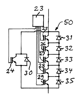
Fig 2 shows very schematically a valve in a Voltage Source
Converter according to the present invention, in which the con-
verter may be a two level converter of the type shown in Fig 1 or
any other type of known Voltage Source Converter. This valve
has one first semiconductor device 24 of turn-off type with a
voltage blocking capacity rating of a first, high level, in the pre-
sent case 6.5 kV, and connected in parallel therewith a series
connection of five second semiconductor devices 25-29 of turn-
,
CA 02710147 2012-02-13
ha
off type with a voltage blocking capacity rating of a second,
- lower level, in this case 1.2 kV. The first semiconductor device
and the second semiconductor devices are in this case IGBTs. A
rectifying diode 30 with a voltage blocking capacity rating of a
third, high level, such as in the order of that of the 1GBT 24, is
connected in anti-parallel with the IGBT 24, and a plurality of
second rectifying diodes 31-35 with a voltage blocking capacity
rating of a fourth, lower level, such as in the order of that of the
IGBTs 25-29, are connected in series and in anti-parallel with
the series connection of the second IGBTs 25-29.
The control arrangement 23 is configured to switch such a valve
into a conducting state starting from a forward biased blocking
state of the valve by controlling the second semiconductor de-
vices 25-29 to be turned on and then said first semiconductor
device 24 to be turned on with a delay sufficient for the voltage
CA 02710147 2010-06-17
WO 2009/092435 PCT/EP2008/050612
12
across the valve to fall to a fraction of less than 10% of the volt-
age across the valve in said forward biased blocking state. This
control arrangement is also configured to at the end of the con-
ducting state turn off the first semiconductor device 24 suffi-
ciently in advance of turning the second semiconductor devices
25-29 off for enabling a majority of recombinations of charge
carriers in the first semiconductor device 24 to take place before
the turning-off of the second semiconductor devices 25-29. This
means that the high voltage IGBT 24 will be turned on at a low
voltage thereacross and turned off before the voltage
thereacross rises to a high level, so that the switching losses of
the semiconductor devices of turn-off type of the valve will be
determined by the switching losses in the second semiconductor
devices 25-29, whereas the conduction losses of the semicon-
ductor devices of turn-off type will be primarily determined by
the conduction losses of the high voltage IGBT 24. For the case
discussed in the introduction this means total losses in the unit
50 shown in Fig 2 of 4500 u compared to 9300 u and 15200 u
when only using the 1.2 kV IGBTs and the 6.5 kV IGBT,
respectively.
Simulations of the voltages and currents in the valve shown in
Fig 2 have been carried out, and the result thereof is shown in
Fig 3 and Fig 4. Fig 3 shows the voltage across the high voltage
IGBT 24 (dashed line) and across the low voltage IGBTs 25-29
(solid line) versus time t, and Fig 4 shows the current through
the high voltage IGBT 24 (dashed line) and the current through
the low voltage IGBTs 25-29 (solid line) versus time. The low
voltage IGBTs 25-29 are turned on at the time to and the high
voltage IGBT 24 at the time t1, when the voltage thereacross is
low. The high voltage IGBT having a lower on-state voltage will
then take over the current through the valve until the point of
time t2, at which the IGBT 24 is turned off and the current com-
mutated into the low voltage IGBTs 25-29, which are then turned
off at the time t3.
CA 02710147 2010-06-17
WO 2009/092435 PCT/EP2008/050612
13
Fig 5 shows schematically a valve of a converter according to
another embodiment of the invention, in which the same refer-
ence numerals as used in Fig 2 have been used in this Figure
for corresponding members. This embodiment differs from the
previous one by the fact that a third semiconductor device 40 of
turn-off type is connected in series with the rectifying member
30 and in parallel with the first semiconductor device 24. This
third semiconductor device is in the present case a MOS tran-
sistor having a low on-state voltage being approximately 0.1 V,
which shall be compared with the forward voltage drop of the
diode 30, which is about 3.5 V.
Furthermore, the number of second semiconductor devices and
second rectifying diodes is in this case six, which is indicated by
the reference numerals 36 and 37.
The control arrangement 23 is configured, when the valve is in a
state in which the current flows through the rectifying diodes
thereof, which will be through the first rectifying diode 30, to
control the MOS transistor 40 to turn off prior to a main
commutation of the current to flow through a valve (the IGBTs
thereof) on the other side of said mid point than said valve for
having the current commutated into the second rectifying diodes
31-36 before such a main commutation. The voltage needed for
commutating the current to flow through the diodes 31-36
instead of through the diode 30 will be approximately 20 V. Said
main commutation will then take place at current flow through
the low voltage diodes 31-36 and not through the high voltage
diode 30 substantially reducing losses created by said
commutation.
Results of simulations carried out for a valve according to Fig 5
are shown in Fig 6 and Fig 7, in which Fig 6 shows the voltage
across the high voltage diode 30 (dashed line) and the voltage
across the low voltage diodes 31-36 (solid line) versus time t,
whereas Fig 7 shows the current through the high voltage diode
CA 02710147 2010-06-17
WO 2009/092435 PCT/EP2008/050612
14
30 (dashed line) and the current through the low voltage diodes
31-36 (solid line) versus time t. It is shown how the MOS
transistor 40 is turned on at the time to and the current is then
transferred to flow through the diodes 31-36, whereupon said
main commutation is carried out at t1.
The invention is of course not in any way restricted to the em-
bodiments described above, but many possibilities to modifica-
tions thereof will be apparent to a person with ordinary skill in
the art without departing from the basic idea of the invention as
defined in the appended claims.
A current valve of the converter according to the invention may
of course be constituted by a number of units 50, 60 shown in
Fig 2 or Fig 5 connected in series, and all first semiconductor
devices thereof are then intended to be controlled
simultaneously, whereas all second semiconductor devices are
intended to be controlled simultaneously.