Note: Descriptions are shown in the official language in which they were submitted.
CA 02710548 2010-06-22
WO 2009/102706 PCT/US2009/033660
ENERGY CONVERSION DEVICE
This application claims priority from U.S. Provisional Application Serial No.
61/065,915, riled February 15, 2008 the contents of which are incorporated by
reference.
The present invention pertains to diode, thermionic, tunneling, and other
devices
that are designed to have very small spacing between electrodes and in some
cases also
require thermal isolation between electrodes. The invention may be applied to
thermo-
tunneling generators and heat pumps, and can be applied to similar systems
using
thermionic and thermoelectric methods. These thermo-tunneling generators and
heat
pumps convert thermal energy into electrical energy and can operate in reverse
to
provide refrigeration. The invention may also be applied to any device that
requires
close, parallel spacing of two electrodes with a voltage applied or generated
between
them.
The phenomenon of high-energy electron flow from one conductor (emitter) to
another conductor (collector) has been used in many electronic devices and for
a variety
of purposes. For example, vacuum-tube diodes were implemented this way, and
the
physical phenomenon was called thermionic emission. Because of the limitations
imposed by the relatively large physical spacing available, these diodes
needed to
operate at a very high temperature (greater than 1000 degrees Kelvin). The hot
electrode
needed to be very hot for the electrons to gain enough energy to travel the
large distance
to the collector and overcome the high quantum barrier. Nevertheless, the
vacuum tube
permitted electronic diodes and later amplifiers to be built. Over time, these
devices were
optimized, by using alkali metals, like cesium, or oxides to coat the
electrodes, in an
effort to reduce the operating temperature. Although the temperatures for
thermionic
generation are still much higher than room temperature, this method of power
generation
has utility for conversion of heat from combustion or from solar concentrators
to
electricity.
Later, it was discovered that if the emitter and the collector were very close
to
each other, on the order of atomic distances like 2 to 20 nanometers, then the
electrons
could flow at much lower temperatures, even at room temperature. At this small
spacing,
the electron clouds of the atoms of the two electrodes are so close that hot
electrons
actually flow from the emitter cloud to the collector cloud without physical
conduction.
This type of current flow when the electron clouds are intersecting, but the
electrodes are
1
CA 02710548 2010-06-22
WO 2009/102706 PCT/US2009/033660
not physically touching, is called tunneling. The scanning tunneling
microscope, for
example, uses a pointed, conducting stylus that is brought very close to a
conducting
surface, and the atomic contours of this surface can be mapped out by plotting
the
electrical current flow as the stylus is scanned across the surface. US Patent
4343993
(Binnig, et al.) teaches such a method applied to scanning tunneling
microscopy.
It has been known in the industry that if such atomic separations could be
maintained over a large area (one square centimeter or even one square
millimeter, for
example), then a significant amount of heat could be converted to electricity
by a single
diode-like device and these devices would have utility as refrigerators or in
recovering
wasted heat energy from a variety of sources. See Efficiency of Refrigeration
using
Thermotunneling and Thermionic Emission in a Vacuum: Use of Nanometer Scale
Design, by Y. Hishinuna, T.H. Geballe, B.Y. Moyzhes, and T.W. Kenny, Applied
Physics Letters, Volume 78, No. 17, 23 April 2001; Vacuum Thermionic
Refrigeration
with a Semiconductor Heterojunetion Structure, by Y. Hishinuna, T.H. Geballe,
B.Y.
Moyzhes, Applied Physics Letters, Volume 81, No. 22, 25 November 2002; and
Measurements of Cooling by Room Temperature Thermionic Emission Across a
Nanometer Gap, by Y. Hishinuma, T.H. Geballe, B.Y. Moyzhes, and T.W. Kenny,
Journal of Applied Physics, Volume 94, No. 7, 1 October 2003. The spacing
between
the electrodes must be small enough to allow the "hot" electrons (those
electrons with
energy above the Fermi level) to flow, but not so close as to allow normal
conduction
(flow of electrons at or below the Fermi level). In some cases, the vacuum gap
might be
used to minimize thermal conductance by lattice phonon vibration and the
filtering of the
hot electrons can take place in a semiconductor or thermoelectric material
adjacent to the
gap as exemplified in International PCT PCT/US07/77042 by the same inventor.
There is
a workable range of separation distance between 0.5 and 20 nanometers that
allows
thousands of watts per square centimeter of conversion from electricity to
refrigeration.
See Efficiency of Refrigeration using Thermotunneling and Thermionic Emission
in a
Vacuum: Use of Nanometer Scale Design, by Y. Hishinuna, T.H. Geballe, B.Y.
Moyzhes, and T.W. Kenny, Applied Physics Letters, Volume 78, No. 17, 23 April
2001.
These references also suggest the advantage of a coating or monolayer of an
alkali metal,
or other material, on the emitting electrode in order to achieve a low work
function in the
transfer of electrons from one electrode to the other. This coating or
monolayer further
reduces the operating temperature and increases the efficiency of conversion
for those
configurations without a separate means for electron filtering.
2
CA 02710548 2010-06-22
WO 2009/102706 PCT/US2009/033660
Mahan showed that the theoretical efficiency of a thermionic refrigerator,
using
electrodes with a work function of 0.7 eV and a cold temperature of 500 K, is
higher than
80% of Carnot efficiency. See Thermionic Refrigeration, By G.D. Mahan, Journal
of
Applied Physics, Volume 76, No. 7, 1 October 1994. Also, see Multilayer
Thermionic
Refrigerator, By G.D. Mahan, J.A. Sofao and M. Bartkoiwak, Journal of Applied
Physics, Volume 83, No. 9, 1 May 1998. By analogy a conversion efficiency of
the
electron tunneling process is expected to also be a high fraction of Carnot
efficiency.
Carnot efficiency presents an upper bound on the achievable efficiency of
thermal energy
conversion.
The maintenance of separation of the electrodes at atomic dimensions over a
large area has been the single, most significant challenge in building devices
that can
remove heat from a conductor. The scanning tunneling microscope, for example,
requires
a special lab environment that is vibration free, and its operation is limited
to an area of a
few square nanometers. Measurements of cooling in a working apparatus have
been
limited to an area of a few square nanometers. See Measurements of Cooling by
Room
Temperature Thermionic Emission Across a Nanometer Gap, by Y. Hishinuma, T.H.
Geballe, B.Y. Moyzhes, and T.W. Kenny, Journal of Applied Physics, Volume 94,
No.
7, 1 October 2003.
More recently, in PCT/US07/77042, devices have been built that achieve much
larger amounts of energy conversion of milliwatts or fractions of watt using a
pair of
bimetal electrodes tested in a vacuum chamber. The device described in this
patent
application, by the same inventor, has been used successfully to form
nanometer gaps in
a bell jar vacuum apparatus such that many materials on either side of the gap
can be
explored and measured. In addition, a fully packaged device with the
successful gap-
forming method of PCT/US07/77042 will be presented here, and this device can
serve as
a fully functional energy conversion product usable outside of a vacuum
apparatus.
Hence, there remains a need for a fully packaged device, which cost-
effectively
and efficiently converts heat energy into electrical energy in a package that
is convenient
to use for both the heat source as input and the electrical circuits needing
power as
output. Abundant sources of heat, including waste heat, could easily become
sources of
electricity. Examples where employing such devices would help the environment,
save
money, or both, include:
(1) Conversion of the sun's heat and light into electricity more cost
effectively
than photovoltaic devices currently used.
3
CA 02710548 2010-06-22
WO 2009/102706 PCT/US2009/033660
(2) Recovery of the heat generated by an internal combustion engine, like that
used in automobile, back into useful motion. Some automobiles available today,
called
hybrid gas-electric automobiles, can use either electrical power or internal
combustion to
create motion. About 75% of the energy in gasoline is converted to waste heat
in today's
internal combustion engine. A tunneling conversion device could recover much
of that
heat energy from the engine of a hybrid automobile and put it into the battery
for later
use. US Patent 6651760 (Cox, et al.) teaches a method of converting the heat
from a
combustion chamber and storing or converting the energy to motion.
(3) Reducing the need for noxious gases to enter the atmosphere. The more
energy-efficient hybrid automobile is a clear example where noxious exhaust
gases
escaping into the atmosphere can be reduced. A device that converts engine and
exhaust
heat of the hybrid engine and then stores or produces electricity in the
hybrid battery
would further increase the efficiency of the hybrid automobile and reduce the
need to
expel noxious gases. Coolants used in refrigeration are other examples of
noxious gases
that are necessary to remove heat, and tunneling conversion devices could
reduce the
need for emission of noxious gases.
(4) Recovery of heat energy at a time when it is available, then storing it as
chemical energy in a battery, and then re-using it at a time when it is not
available.
Tunneling conversion devices could convert the sun's energy to electricity
during the
day and then store it in a battery. During the night, the stored battery power
could be
used to produce electricity.
(5) Power generation from geothermal energy. Heat exists in many places on the
surface of the earth, and is virtually infinitely abundant deep inside the
earth. An efficient
tunneling conversion device could tap this supply of energy.
(6) Production of refrigeration by compact, silent and stationary solid state
devices, where such a tunneling device could provide cooling for air
conditioners or
refrigeration to replace the need for bulky pneumatic machinery and
compressors.
(7) Power generation from body heat. The human body generates about 100 watts
of heat, and this heat can be converted to useful electrical power for
handheld products
like cell phones, cordless phones, music players, personal digital assistants,
and
flashlights. A thermal conversion device as presented in this disclosure can
generate
sufficient power to operate or charge the batteries for these handheld
products from heat
applied through partial contact with the body.
4
CA 02710548 2010-06-22
WO 2009/102706 PCT/US2009/033660
(8) Electrical power from burning fuel. A wood stove generates tens of
thousands
of watts of heat. Such a tunneling device could generate one or two kilowatts
from that
heat which is enough to power a typical home's electric appliances. Similar
applications
are possible by burning other fuels such as natural gas, coal, and others.
Then homes in
remote areas may not require connection to the power grid or noisy electrical
generators
to have modern conveniences.
The challenge in bringing two parallel electrodes together within less than
20.0
nanometer separation gap and the proposed solution by this inventor and others
is well
described in PCT/US07/77042 and in "Analysis of nanometer vacuum gap formation
in
thermo-tunneling devices ", by E T Enikov and T Makansi, Nanotechnology
Journal,
2008. Here, we will focus on a fully packaged device with its own vacuum
chamber that
can be manufactured at a low cost for mass production and competitively priced
relative
to compressors, turbines, and electrical generators. This device contains
within it the
gap-forming bimetal electrode design summarized in PCT/US07/77042.
The art of separating two conductors by about 2.0 to 20.0 nanometers over a
square centimeter area has been advanced by the use of an array of feedback
control
systems that are very precise over these distances. A control system includes
a feedback
means for measuring the actual separation, comparing that to the desired
separation, and
then a moving means for bringing the elements either closer or further away in
order to
maintain the desired separation. The feedback means can measure the
capacitance
between the two electrodes, which increases as the separation is reduced. The
moving
means for these dimensions is, in the state of the art, an actuator that
produces motion
through piezoelectric, magnetostriction, or electrostriction phenomena. U.S.
Patents
6,720,704 (Tavkhelidze, et al.) and 7,253,549 (Tavkhelidze, et al.) and US
Patent
Application No. 2007/0033782 (Taliashvili et al.) describes such a design that
includes
shaping one surface using the other and then using feedback control systems to
finalize
the parallelism prior to use. Because of the elaborate processes involved in
shaping one
surface against the other and the use of multiple feedback control systems to
maintain
parallelism, this design approach is a challenge to manufacture at a low cost.
Other methods have been documented in US Patents 6,774,003 (Tavkhelidze, et
al.), and 7,140,102 (Taliashvili , et al.), and US Patent Applications
2002/0170172
(Tavkhelidze, et al.), 2006/0038290 (Tavkhelidze, et al.), and 2001/0046749
(Tavkhelidze, et al.) that involve the insertion of a "sacrificial layer"
between the
electrodes during fabrication. The sacrificial layer is then evaporated to
produce a gap
5
CA 02710548 2010-06-22
WO 2009/102706 PCT/US2009/033660
between the electrodes that is close to the desired spacing of 2 to 20
nanometers. These
three methods are either susceptible to post-fabrication fluctuations due to
warping or
thermal expansion differences between the electrodes, or require the array of
actuators to
compensate for these fluctuations, as described in US Patent Application Nos.
2005/0189871 (Tavkhelidze, et al.) and 2007/0056623 (Tavkhelidze, et al.).
Another method of achieving and maintaining the desired spacing over time is
documented in US Patents 6,876,123 (Martinovsky, et al.) and 7,305,839
(Weaver) and
6,946,596 (Kucherov , et al.) in US Patent Application Nos. 2004/0050415,
2006/0192196 (Tavlhelidze, et al.), 2003/0042819 (Martinovsky, et al.),
2006/0207643
(Weaver et al.), 2007/0069357 (Weaver et al.), and 2008/0042163 (Weaver)
through the
use of dielectric spacers that hold the spacing of a flexible electrode much
like the way
poles hold up a tent. One disadvantage of these dielectric spacers is that
they conduct
heat from one electrode to the other, reducing the efficiency of the
conversion process.
Another disadvantage of this method is that the flexible electrodes can
stretch or deform
between the spacers over time in the presence of the large electrostatic
forces and
migrate slowly toward a spacing that permits conduction rather than tunneling
or
thermionic emission. Some of the challenges of forming a nanometer gap with
these
methods is summarized in " Thermotunneling Based Cooling Systems for High
Efficiency
Buildings ", by Marco Aimi, Mehmet Arik, James Bray, Thomas Gorczyca, Darryl
Michael, and Stan Weaver, General Electric Global Research Center, DOE Report
Identifier DE-FC26-04NT42324, 2007.
Another method for achieving a desired vacuum spacing between electrodes is
reveled in US Patent Application Nos. 2004/0195934 (Tanielian) , 2006/0162761
(Tanielian), 2007/0023077 (Tanielian), 2007/0137687 (Tanielian), and
2008/0155981
(Tanielian) wherein small voids are created at the interface of two bonded
wafers. These
voids are small enough to allow thermo-tunneling of electrons across a gap of
a few
nanometers. Although these gaps can support thermo-tunneling, unwanted thermal
conduction takes place around the gaps, and the uniformity of the electrode
spacing is
difficult to control.
Yet another method for achieving a thermo-tunneling gap is by having the
facing
surfaces of two wafers be in contact, then using actuators to pull them apart
by a few
nanometers, as described in U.S. Patent Application 2006/0000226. Although
this
method can produce a thermo-tunneling gap, this method suffers from the cost
of
multiple actuators and the thermal conduction between wafers outside of the
gap area.
6
CA 02710548 2010-06-22
WO 2009/102706 PCT/US2009/033660
The present disclosure provides improvements in the packaging, fabrication,
and
more specific implementation detail of the gap-forming designs described in
PCT/US07/77042. Four package design approaches are presented, each trading off
cost
and reliability uniquely. The first and preferred package design uses flexible
glass and
flexible silicon to serve simultaneously as the vacuum wall, the electrode
substrate, and
optionally the circuit board for interconnect. The second package design uses
all glass
substrates with metal inserts. The third package design employs a flexible
plastic
material that is a vacuum-compatible offering lower cost, but less reliability
due to
plastic out-gassing, lower wall rigidity, and some porosity. The fourth
package design
employs a thick glass wall that is not flexible and hence the gap-forming
mechanism is
less disturbed by external vibration or shock. However, this design is more
costly to
manufacture.
For each of the four designs, two embodiments are possible. In one embodiment,
each tunneling junction has its own vacuum chamber, and a separate connector
is
required to provide the interconnecting of multiple junctions. In the second
embodiment,
multiple junctions share a vacuum chamber with the interconnecting also
contained
within. Without limitation, the diagrams will show the multiple junction
embodiments of
which the single junction embodiment is a subset.
A surface roughness of less than 1.0 nanometer can be achieved by any of
several
techniques known to the industry. Even though silicon and glass wafers are
routinely
polished to sub-nanometer roughness, the deposition of metal films creates
additional
roughness from nucleation and grain formation. This surface roughness can then
be
removed by (1) using a post-polishing process such as chemical mechanical
polish called
CMP, (2) cooling the substrate during deposition to prevent or minimize grain
formation,
or (3) pressing the surface against a known smooth surface such as that of a
raw wafer.
These and other polishing techniques are readily available in the industry for
achieving
less than 1.0 nanometers surface roughness on metals, semiconductors, and
other
materials.
Other systems, devices, features and advantages of the disclosed device and
process will be or become apparent to one with skill in the art upon
examination of the
following drawings and detailed description. It is intended that all
additional systems,
devices, features, and advantages be included within this description, be
within the scope
of the present invention, and be protected by the accompanying claims.
7
CA 02710548 2010-06-22
WO 2009/102706 PCT/US2009/033660
Many aspects of the disclosed device and process can be better understood with
reference to the attached drawings. The components in the drawings are not
necessarily
to scale, emphasis instead being placed upon clearly illustrating the
principles of the
present invention. Moreover, in the drawings, like reference numerals do not
need
corresponding parts throughout the several views. While exemplary embodiments
are
disclosed in connection with the drawings, there is no intent to limit the
disclosure to the
embodiments disclosed herein. On the contrary the intent is to cover all
alternatives,
modifications and equivalents.
FIG. la and FIG. lb illustrate a single junction of the present invention with
one
curved electrode and one flat electrode with contact in the center; FIG. la is
a profile
view, and FIG. lb illustrates regions of the interior surface;
FIG. 2a and FIG. 2b illustrate a single junction, but with corner posts added
in
order for the center contact to be replaced with a nanometer gap under certain
operating
conditions. FIG. 2a is a profile view, and FIG. 2b illustrates regions of the
interior
surface;
FIG 3a shows how the junction of FIGS. la and lb or FIGs. 2a and 2b can be
used to provide refrigeration upon electrical activation, and FIG. 3b
alternatively shows
how these same devices can be used to convert heat to electricity'
FIG. 4a through FIG. 4d show how a plurality of junctions connected in series
electrically can come together in a single vacuum package where silicon serves
as the
flexible substrates as well as a partial vacuum wall, and flexible glass
serves as a thermal
isolator as well as the remaining vacuum wall;
FIG. 5a and FIG. 5b show more detail of the device of FIG. 4 in a profile view
including the stack of films to create the thermoelectric junctions and to
connect them
together;
FIG. 6 shows an alternative embodiment to FIG 5a and Fig. 5b using flexible
glass as the substrates and the vacuum walls, and with metal inserts in the
glass to
improve thermal conduction away from the junction;
FIG. 7 shows another alternative embodiment to FIG. 5a and FIG. 5b using a
flexible, vacuum-compatible plastic as the vacuum wall and separate silicon
dice as the
substrates;
FIG. 8a and FIG. 8b show another alternative embodiment to FIG. 5a and FIG.
5b using rigid glass as the vacuum wall and flexible silicon as the substrate.
FIG. 9a
8
CA 02710548 2010-06-22
WO 2009/102706 PCT/US2009/033660
illustrates an arrangement for decreasing the curvature in the center of a
bimetal
arrangement (which in turn increases the active area of tunneling) by removing
some
material, which may be applied to any or all of the embodiments of Fig. I
through FIG.
8;
FIG. 9b plots radius of curvature and radius of hole;
FIG. I Oa and FIG. I Ob show other geometric configurations that are analogous
to
FIG. la and FIG, lb and FIG. 2a and FIG. 2b in providing a small contact area
combined
with a larger tunneling area for electron flow;
FIG. 11 illustrates a device similar to that shown in FIG. 2a; and
FIG. 12 is a plot of Peltier coefficient against Chip Temperature.
The figure of merit for a thermoelectric device is
ZT = a2T/KR
a is the Seebeck coefficient in volts per degree of temperature difference, T
is the
temperature in Kelvin, K is the thermal conduction in watts per degree of
temperature
difference, and R is the electrical resistance. The electrical resistance R
can further be
expressed as
R = pL/Ae
p is the electrical resistivity of the thermoelectric material, L is the
length that the
electrons must travel in this material, and Ae is the cross-sectional area of
the electron
flow. The thermal conduction K can be further expressed as
K = (KeAe + K,Ai)/L
L is again the length of the material. Two mechanisms exist for heat
conduction in a
metal or semiconductor, one due to electron flow and the other due to phonon
flow. The
heat conduction due to phonon flow is also called lattice thermal conduction.
In this
equation, Ke is the thermal conductivity component due to electrons and Ae is
the cross-
sectional area over which electrons can flow, as before. K, is component of
thermal
conductivity due to phonons and A, is the cross-sectional area through which
phonons
can flow, Substituting the expressions for R and K into the formula for ZT
yields the
following equation:
ZT = (x 2TAe/Cp(KeAe + iciA,)]
In thermoelectric materials and for traditional thermoelectric devices Ae =
A,, and hence
KR = Kp.
9
CA 02710548 2010-06-22
WO 2009/102706 PCT/US2009/033660
In a thermoelectric device, it is desirable to minimize electrical resistance
to reduce
electrical losses, which affects efficiency. It is also desirable to minimize
thermal
conduction so that losses due to heat backflow from the hot side to the cold
side are
minimized. A traditional thermoelectric device only allows electrons to
conduct through
the thermoelectrically active material. In one embodiment of this invention
illustrated in
FIG. la and FIG. lb, electrons and phonons conduct though a portion of the
cross-
sectional area, but only electrons are able to tunnel through a much larger
area. By
having a larger area for electron flow than for phonon flow, the performance
of the
device can be increased significantly. An important part of this invention is
a device
wherein Ai can be less than Ae and this difference leads to a higher ZT and a
higher
efficiency and performance.
In another embodiment of this invention illustrated in FIG. 2, no phonon
transfer
is possible, but electrons are still able to tunnel over the entire cross-
sectional area,
increasing performance and efficiency even further than illustrated in FIG, la
and FIG
1 b. In this case Ai is zero, leading to an even higher ZT, efficiency, and
performance.
Referring more specifically to the drawings in which like reference numerals
refer to like elements throughout the several views, exemplary embodiments of
the
device and process of the present disclosure are illustrated in FIGs. 1-12.
In FIG. I a, two electrodes are shown, one curved and the other essentially
flat. A
piece of single-crystal silicon 100 serves as the substrate, and this
substrate is highly
doped to levels of 0.001 to 0.01 ohm-em to allow electrical conductivity from
top to
bottom. Without limitation, other semiconductors could be used for substrate
100 such as
silicon carbide, germanium, and gallium arsenide. Both types of metal layers
101 and
102 serve to spread the electrical current allowing this current to flow
across the entire
area of the silicon substrate 100, thereby reducing resistance of current flow
from the top
of the device to the bottom. Metal layer 101 is thicker, or laterally larger,
or both thicker
and laterally larger than metal layer 102. Layer 103 is the thermoelectrically
active
material. Depositing metal layer 101 on or otherwise adhering it to silicon
substrate 100
at an elevated temperature forms the curved upper electrode. As the pair of
layers 100
and 101 cool down to room temperature after deposition or adhesion, the
greater thermal
contraction of metal 101 relative to silicon 100 introduces mechanical
stresses that give
rise the curved shape shown. This curvature occurs in both lateral dimensions,
making
CA 02710548 2010-06-22
WO 2009/102706 PCT/US2009/033660
the curved shape a dome, although FIG. la shows only a profile view. Without
limitation, other arrangements for achieving a curved surface are included
such as
micromachining or pulling forces of an interior vacuum cavity.
In operation, the two electrodes in FIG. I a are spring loaded to push against
each
other, and the apparatus in this figure is placed in a vacuum chamber. To
activate the
device for cooling, a voltage is applied between the very top 101 and very
bottom 102
metal layers 102. This voltage gives rise to a current flow through the
thermoelectrically
active layer 103 and this current moves heat either in the same direction of
the current if
the material 103 is p-type or in the opposite direction as the current if
material 103 is n-
type material. To activate the device for power generation, heat is applied to
the lower
electrode, giving rise to a temperature gradient between the lower and upper
electrodes
and this gradient produces a voltage, called the Seebeck voltage, between the
top and
bottom electrodes.
The central portion 107 of the invention illustrated in FIG. la is similar to
a
traditional thermoelectric device with one unique exception, which is a key
aspect of this
invention. In a standard thermoelectric device, active layer 103 in central
portion 107
would be continuous from top to bottom. In the invention device, active layer
103 has
some continuity vertically through a contact area 104 illustrated in FIG, lb.
In this
contact area 104, both electrons and phonons can conduct heat, and electrons
can
conduct electricity. The area 105 surrounding the contact area 104 is of
particular
interest. The geometry of the device is designed such that electrons are able
to tunnel in
non-contact vacuum-gap area 105, but phonons are not able to flow at all due
to
interruption of the crystal lattice with a vacuum layer. Hence the area of
electron flow
105 is larger than the area of phonon flow 104. Area 106 is the total area of
the silicon
substrate, which may include an area where neither electrons nor phonons can
flow
because the vacuum gap is too large for electrons to tunnel.
To estimate the figure of merit ZT improvement of the device of FIG. la, the
active layer material 103 will be assumed to be Bi2Te3, the most widely used
thermoelectric material. Furthermore, the operating temperature T will be
assumed to be
room temperature or 300 Kelvin. The following parameter values are well
published for
this material: a = 260 microvolts per degree Kelvin, p = 0.001 ohm-centimeter,
xe = 0.4
watts/meter-degree Kelvin, K1 = 1.6 watts/meter-degree Kelvin. For a
traditional
thermoelectric device, Ae = A,. Substituting these values into the formula for
ZT
11
CA 02710548 2010-06-22
WO 2009/102706 PCT/US2009/033660
ZT = a2TAe/[P(KeAe + K A )]
The formula for ZT computes to a value of 1.04, which is the published and
commonly cited ZT performance for Bi2Te3 devices when Ae = A,. If we now refer
to
FIG. 1 a and FIG. I b, and assume that the area of phonon flow 104 has a
radius that is
four times lower than the radius of electron flow 105, then A,/A, is 1/16
which yields
from the equation ZT = 4.06. Hence we see that for the embodiment illustrated
in FIG.
1 a and FIG. lb that the figure of merit ZT for the thermoelectric performance
can be
approximately four times higher than for traditional devices. Without
limitation, more
complex thermoelectric materials may substitute for Bi2Te3. One example of a
complex
thermoelectric material is a super-lattice, which is a thermoelectric film
comprised of
multiple very thin films, the borders of which reduce the lattice thermal
conduction.
Other examples of complex thermoelectric materials include clathrates and
chalcogenides. A comprehensive review of complex thermoelectric materials is
provided
in Complex Thermoelectric Materials, by G. Jeffrey Snyder and Eric S. Tober,
Nature
Materials, Vol. 7, February 2008.
FIG. 2a and FIG 2b show a variation on the embodiment of FIG. la and FIG. lb
where four separators 108 are placed between the electrodes in each of the
four corners.
Only two of these separators are shown because FIG. 2a is a profile view.
These
separators may be made of glass or other dielectric material preferably with
low thermal
and electrical conductivity. The height of separators 108 is selected such
that as the
upper electrode heats up, the thermal expansion differences the silicon and
the metals
cause the upper electrode to flatten, ultimately forming a gap in the center,
as the corner
separators become the supports. If the gap of FIG 2a is controlled to create a
I nm or less
vacuum layer between the two electrodes, then the contact area illustrated by
104 in FIG.
lb is eliminated, and all phonon flow is blocked. However, electrons are able
to tunnel in
area 105. In this case, A, = 0 and the formula for ZT
ZT = a2TAe/[p(Ks0Ae + K1A1)]
yields a ZT of 5.07 for the material parameters quantified above for Bi2Te3
and at room
temperature.
The ZT calculations for the invention presented thus far assume the
characteristics of the thermoelectric material Bi2Te3 that is widely used
today for
traditional thermoelectric devices. In the case of the embodiment illustrated
in FIG. 2a
12
CA 02710548 2010-06-22
WO 2009/102706 PCT/US2009/033660
and FIG. 2b, the lattice thermal conductivity of the thermoelectric material
is irrelevant
because the vacuum gap area 105 prevents all phonon flow. The center contact
approach
illustrated in FIG. la and FIG. lb prevents most of the phonon flow. For these
reasons,
the optimal thermoelectric material for the invention might not be Bi2Te3,
which has
evolved as the optimum for traditional devices. Including those materials that
have large
or larger lattice thermal conductivity can enlarge the space of candidate
materials for the
invention device. These new material possibilities are important for many
reasons.
Elements in the periodic table with low lattice thermal conductivity are those
with
relatively large atomic weights. Semiconductors and metals with relatively
large atomic
weights tend have the following undesirable properties: (1) toxicity, (2)
radioactive, (3)
high cost, (4) scarcity in either natural or man-made forms, and (5) inability
to withstand
higher temperatures.
For example, toxicity is a major concern for traditional thermoelectric
materials.
Tellurium and similar elements like Antimony that are used in traditional
devices are
toxic. Silicon and Germanium are semiconductors that are non-toxic, plentiful,
and
inexpensive. Silicon and Germanium are not used in traditional thermoelectric
devices,
however, because their lattice thermal conductivities are several times higher
than
Tellurium and Antimony. Silicon and Germanium would work just fine in the
embodiment of FIG. 2a and FIG. 2b because lattice thermal conduction is
minimized by
the vacuum gap.
Also, in order for thermoelectric devices to be used in power generation, the
desire is great to operate them at high temperatures. The laws of
thermodynamics state
that the higher the temperature delta in an engine, the higher the efficiency
of that
engine. Very high temperatures, approaching 1000 Kelvin are required to
maintain high
efficiency power generators, and these temperatures are routinely used in
power plant
engines fueled by coal, gas, or nuclear energy. Thermoelectric devices need to
sustain
these same temperatures in order to compete with existing power plants.
Bismuth,
Tellurium, and Antimony have melting points of 555K, 723K, and 904K
respectively.
Because of these low melting points, the operational temperature of
traditional
thermoelectric devices has been limited to 500K. If the hot side of the device
is 500K
and the cold side is cooled to room temperature. or 300K, then the theoretical
maximum
efficiency is 40%, and that assumes an infinite ZT. However, silicon and
germanium
have melting points of 1693K and 1211K, and hence can sustain the temperatures
of up
13
CA 02710548 2010-06-22
WO 2009/102706 PCT/US2009/033660
to 1000K required to compete with existing power plants in thermodynamic
efficiency.
For details of thermoelectric performance of silicon-germanium, see Thermal
and
electrical properties of Czochralski grown GeSi single crystals, by I.
Yonenaga et. al.
Journal of Physics and Chemistry of Solids 2001. For details about the surface
behavior
of these materials, see "Selective Epitaxial Growth of SiGe on a SOI Substrate
by Using
Ultra-High-Vacuum Chemical Vapor Deposition ", by H. Choi, J. Bae, D. Soh, and
S.
Hong, Journal of the Korean Physical Society, Vol. 48, No. 4, April 2006, pp.
648-652
and "Strain relaxation of SiGe islands on compliant oxide ", by H. Yin et. al.
Journal of
Applied Physics, vol. 91, number 12, 15 June 2002.
Another advantage of the invention is the ability to operate over a range of
temperatures, For traditional thermoelectric devices, Bi2Te3 and similar
materials are
used at low temperatures (lower lattice thermal conductivity, but lower
melting points)
and other materials like SiGe are used at higher temperatures (higher lattice
thermal
conductivity but higher melting points). The present invention allows a
material such as
SiGe to be used at the full range of temperatures because lattice thermal
conduction is
partially or totally eliminated by the vacuum gap illustrated in FIG. la and
FIG, lb and
FIG. 2a and FIG.2b.
Thermoelectric devices are generally reversible, meaning that a current flow
through the device will produce refrigeration and, conversely, applying heat
to one side
will produce a voltage. The device of this invention is also reversible, and
FIG. 3a and
FIG. 3b show the preferred configuration for each of the two modes of
operation. FIG.
3a shows the preferred configuration for refrigeration, and FIG, 3b shows the
preferred
configuration for power generation from heat.
In FIG. 3a, the curved bimetallic electrode 113 with the thick copper layer is
the
hot side. A voltage source 109 supplies a voltage to the top and bottom of the
device
through wires 110. This voltage produces a current flow through the
thermoelectric
material in the center of the device, and this current flow moves heat from
the bottom
electrode to the top electrode assuming that the thermoelectric material used
is n-type.
Without limitation, a similar diagram could be made with current flowing
oppositely by
reversing the applied voltage 109, and with a p-type material, the heat would
still flow
from the bottom electrode to the top electrode.
When the device of FIG. 3a is turned off, the voltage 109 is zero, and central
contact exists between the two electrodes. The flow of current moves heat to
the top
electrode, increasing its temperature. This increased temperature causes the
top electrode
14
CA 02710548 2010-06-22
WO 2009/102706 PCT/US2009/033660
to flatten out which eventually creates a gap in the center and the top
electrode now uses
the corner separators for support. The gap in the center will increase in size
until it
reaches an equilibrium value. If a disturbance causes the gap to become larger
than the
equilibrium value, then less current will flow because the gap is opening the
circuit
between the two electrodes. Less current means less heat is moved to the upper
electrode,
lowering its temperature, and bending back toward the bottom electrode until
the
equilibrium is re-established. Conversely, if a disturbance causes the gap to
be smaller
than its equilibrium value, then more current will flow, moving more heat,
increasing the
temperature of the top electrode, and bending it away from the bottom
electrode until
again the equilibrium is re-established.
The device of FIG. 3a can be applied to thermoelectric cooling methods, also
called the Peltier effect, by choosing active layer 103 to be a
thermoelectrically sensitive
material. Bimuth Telluride, Antimony Bismuth Telluride, Lead Telluride,
Silicon
Germanium, and many other materials are known to exhibit the thermoelectric
effect,
without limitation. In the case of thermoelectric methods applied to the
device of FIG.
3a, the gap can be barrier-free, meaning that electrons do need higher than
average
energy to traverse the gap. The quantum barrier of the bandgap of the
thermoelectric
material 103 already filters higher energy electrons which enables heat to be
moved. So,
in this case, the nanometer gap between the two active layers 103 merely needs
to
interrupt the lattice thermal conduction, The device of FIG. 3a can also be
applied to
thermo-tunneling cooling methods by choosing active layer 103 to be a low work
function material. Examples of low work function materials are Cesium, Barium,
Strontium and their oxides. The layer 103 could take the form of a monolayer,
sub-
monolayer, multiple monolayers, or deposited film. In the case of thereto-
tunneling
methods applied to the device of FIG. 3a, the gap length does introduce a
barrier over
which only higher energy electrons can traverse. In thermo-tunneling
applications, the
nanometer gap serves as both the quantum barrier to filter electrons and also
as an
interruption of the lattice thermal conduction.
In the preferred configuration for power generation in FIG. 3b, note that the
curved, bimetallic electrode is now the cold side, Heat is applied to the flat
electrode
from a heat source 111. Because the temperature of the heat source might vary
during
operation, as in a concentrated solar application for example, it is
preferable to apply the
heat to the side that would not vary the gap from its optimal value. As is
typical in
thermoelectric devices, the heat source 111 creates a temperature gradient
within the
CA 02710548 2010-06-22
WO 2009/102706 PCT/US2009/033660
thermoelectrically sensitive material, which in turn creates a voltage that
can be brought
to an electrical circuit needing power 112 through wires 110.
When no heat is applied at heat source 1 11, center contact exists between the
two
electrodes. As the heat source is turned on, some of this heat will flow
through the center
contact, increasing the temperature of the top electrode 1] 3. The increased
temperature
causes the top electrode 113 to flatten out, ultimately creating a gap in the
center as the
top electrode then rests on the corner separators 108. As in the case for
refrigeration, an
equilibrium gap is formed. If a disturbance causes the gap to become larger
than
equilibrium, then the top electrode will cool down because of less heat
traversing the
gap, which causes the top electrode 113 to bend toward the bottom electrode,
and re-
establish the equilibrium. If a disturbance causes the gap to become smaller
than
equilibrium, then the increased heat conduction in the center will increase
the
temperature of the top electrode, causing it to bend away in the center until
the
equilibrium gap is re-established.
The device of FIG. 3b may be applied to thermoelectric power generation
effects,
also called the Seebeck effect, by choosing active layer material 103 to be a
thermoelectrically sensitive material. Again, without limitation, the same
materials
mentioned earlier that exhibit the Peltier effect also exhibit the Seebeck
effect. The
device of FIG. 3b may also be applied to thermo-tunneling power generation by
choosing the active layer 103 to be a low work function material. Without
limitation, the
same materials useful for thermo-tunneling cooling are also useful for thermo-
tunneling
power generation. The device of FIG. 3b may also be applied to thermo-
photovoltaic
methods by choosing lower active layer material 103 to be photo-emissive and
the upper
layer 103 to be photosensitive. , Photo-emissive materials emit photons in
response to the
application of heat. Photosensitive materials generate electricity upon the
receipt of
photons. Photons are also capable of tunneling across a vacuum gap such as the
one
illustrated in FIG. 3b, thereby converting heat to electricity while retaining
thermal
isolation. The required gap length for photon tunneling is typically much less
than the
wavelength. For visible light, the wavelength is 400 to 700 nanometers, so a
gap length
of 1 nm to 200 nm is sufficiently small for effective photon tunneling.
Without
limitation, examples of photo-emissive materials are tungsten and titanium.
Also without
limitation, examples of photosensitive materials include photovoltaic
materials such as
silicon, germanium, tellurium, cadmium and combinations of these. For a
summary of
thermo-photovoltaic methods, see Micron-gap ThermoPhotoVoltaics (MTPV), by R.
16
CA 02710548 2010-06-22
WO 2009/102706 PCT/US2009/033660
DiMatteo et al, Thermophotovoltaic Generation of Electricity, American
Institute of
Physics, 2004.
The previous figures FIG. 1 through FIG. 3 showed the preferred embodiments
for a single thermoelectric junction. FIG. 4a to FIG. 4d show how a plurality
of junctions
can be fabricated using standard silicon substrates with deposited metal
films, with the
hot.and cold sides vacuum-sealed together using standard wafer bonding
processes and
equipment.
FIG. 4a shows how the top substrate 115 comes together with bottom substrate
116 with glass frame 114 in between. These three components 115, 116, and 114
also
comprise the walls of the vacuum chamber. The top 115 and bottom 116 are each
attached to the glass frame 114 using glass frit or other vacuum sealing
adhesives along
the overlapping perimeter. The bottom substrate 116 extends out beyond the
glass frame
and beyond the vacuum seal in order to expose electrical connections 120.
These
electrical connections allow the device to be connected to an electrical power
supply for
refrigeration or to an electrical load for power generation. Bottom silicon
substrate 116
in FIG. 4d serves as the carrier for the thermoelectric stacks 118 and 203 and
associated
interconnect circuitry 117. Note how, in contrast with FIG. Ia and FIG. lb and
FIG. 2a
and FIG. 2b, the electrical current does not need to flow through the silicon
substrate in
FIG 4a and FIG, 4b. The silicon substrate used in this embodiment of FIG. 4a
and FIG.
4b is un-doped or lightly doped to prevent the silicon from becoming short
circuits. This
substrate 116 in FIG. 4d also serves as the bottom of the vacuum package. The
top
silicon substrate 115 in FIG. 4c is has thick metal pads 101. These pads are
deposited or
adhered to the silicon substrate 115 at a high temperature so that at room
temperature and
at operating temperatures, a local curvature exists caused by bimetallic
stresses between
thick metal 101 and silicon substrate 115. The top substrate also has
thermoelectric
stacks, which face the thermoelectric stacks of the bottom substrate 103 and
118 in FIG.
4d. The thermoelectric stacks for the top substrate are not visible in FIG.
4c. The primary
function of the glass frame 114 in FIG. 4b is to minimize the heat conduction
between
the hot and cold sides, as glass has a much lower thermal conductivity than
silicon. A
direct face-to-face perimeter bond of the top and bottom silicon substrates
would have
high thermal conduction, decreasing performance. The side width of the glass
frame 114
in FIG. 4b can be selected to achieve the desired amount of thermal isolation.
FIG. 5a shows a profile view of the device of FIG. 4 including detail about
the
film stack. The inset in FIG. 5b is a blow-up view of FIG. 5a. Glass frame 114
is bonded
17
CA 02710548 2010-06-22
WO 2009/102706 PCT/US2009/033660
and vacuum-sealed to the top substrate 1 l 5 using perimeter sealant 121,
which might be
glass frit, solder, compression bond, or other suitable material. A similar
perimeter
sealant 121 bonds the glass frame 114 to the bottom substrate. Pad 120 is
externally
exposed for electrical connection purposes. Getter 122 is positioned within
the vacuum
cavity to react with any residual, out-gassed, or leaked-in gases during the
life of the
device, helping to maintain close to ideal vacuum conditions. Electrical
traces 117
connect the thermoelectric pads to each other and to the external pads.
Optional glass
posts 108 serve as corner separators for each thermoelectric stack during
operation when
a gap is formed. When the device is turned off, the center contact of the
thermoelectric
stacks provide support against the vacuum pressure pulling the top and bottom
electrodes
together. Film 101 is a thick film with a thermal expansion coefficient that
is higher than
for the substrate 115. This film 101 is deposited or bonded to substrate 115
at an elevated
temperature for reasons described earlier. Copper, aluminum, tin, and many
other metals
and alloys are appropriate for film 101. Film 119 is a thin layer of another
metal such as
titanium, tungsten, or other alloy that provides good adhesion between the
thick film 101
and the substrate 115. Without limitation, other adhesion layers are known to
the art.
The films deposited on the interior portion of the device will now be
described.
Adhesion layer 102 provides good adhesion between substrate 115 or 116 and the
film
102, which has high electrical conductivity. Film 102 carries most of the
electrical
current from one thermoelectric stack to the next and to the external
connections. Film
118 is the thermoelectrically active layer, which may be a semiconductor, an
oxide, or a
low work function material, photosensitive or photo-emissive layer as
previously
described.
Because low voltage and high current characterize thermoelectric junctions,
most
thermoelectric devices internally connect the junctions in series. By having
many series
connected junctions, the available supply or load voltage can better match a
sum of
individual junction voltages. These series connections mean that the heat must
flow with
the current in the p-type junctions and against the current in the n-type
junctions.
The preferred material for thermoelectric film 103 of FIG. 4d is in cooling
configurations Bismuth Telluride for the n-type stacks and Antimony Bismuth
Telluride
for the p-type stacks. Film 118 in FIG. 4d and FIG. 5b show an example of how
the p-
type material if used in contrast with the n-type material 103. For power
generation
operation, the preferred material for film 103 and 118 is Silicon Germanium,
each with
differing compositions. Without limitation, the material for film 103 can also
be a super-
18
CA 02710548 2010-06-22
WO 2009/102706 PCT/US2009/033660
lattice thermoelectric material, a quantum well, appropriately doped
semiconductor, or
other thermoelectric material.
FIG. 6 shows an alternative embodiment to the device of FIG. 4a and FIG. 4b
and
FIG. 5a and FIG. Sb. Glass 124 is used as both the top and bottom substrates.
Because
glass has much lower thermal conductivity (I watt/meter-degree) as compared to
silicon
(150 watts/meter-degree), another means is useful to conduct heat away from
the
thermoelectric junctions to the outside. Metal inserts 123 in the glass
substrates 124
provide this means, and a highly thermal conducting path now exists from the
thermoelectric junction to the outside. Metal inserts 123 also optionally
provide an
electrical path to connect the thermoelectric junctions together using metal
traces 117.
These metal traces may be located on the inside or the outside of the vacuum
cavity
defined by the substrate top and bottom. The thick metal pads 101 provide the
bimetallic
arrangement and produce curvature as before. The remainder of the parts and
operation
of the device of FIG. 6 is evident from the very similar diagram in FIG. 4a
and FIG. 4b
and FIG. 5a and FIG. 5b.
FIG. 7 shows another alternative embodiment to the device of FIG. 4a and FIG.
4b and FIG. 5a and FIG. 5b using a flexible plastic vacuum wall 127. Flexible
plastic
materials like polyimide and Kapton are known to be very low out-gassing and
hence
compatible with vacuum environments. In FIG. 7, silicon substrates 100,
optional glass
posts 108, and bimetallic arrangements are used as before. The polyimide
vacuum walls
127 have electrical traces 117 that provide the connections between the
thermoelectric
stacks and to the external connections using a through-hole 126 and a solder
pad 125 for
easy electrical connection to wires. A vacuum seal 125 is provided around the
perimeter.
One way to achieve this perimeter vacuum seal is to place a copper or similar
metal trace
128 and use solder 125 as the sealant. Without limitation, other sealing
techniques may
also be applied. Polyimide is known to be porous, and a thin layer of non-
porous material
such as a metal film or silicon dioxide or other film may be required (not
shown).
The embodiments shown in FIG. 4 through FIG. 7 all use a flexible material as
the vacuum wall. For some implementations, particularly in harsh environments,
a rigid
package might be desired or required. FIG. 8a and FIG. 8b show an alternative
embodiment where the vacuum walls are rigid glass substrates 129. Rigid
silicon
substrates 100 are exposed by holes 131 in the glass to provide electrical and
thermal
connections to the outside. In the fabrication of the device of FIG. 8a and
FIG. 8b, the
19
CA 02710548 2010-06-22
WO 2009/102706 PCT/US2009/033660
upper and lower substrates 129 start as glass wafers with holes 131. These
substrates
serve as the top and bottom of the vacuum cavity, except in the holes 131
wherein silicon
substrates 100 are vacuum-sealed around the perimeter of these holes. A glass
lattice 130
is inserted between the upper and lower substrates and is perimeter-bonded
with a
vacuum seal. The bimetal configuration is achieved by the middle silicon die
100 in
combination with its thick metal layer 101 and is electrically connected to
the rigid
silicon die by a metal bump 134. Flexible thermal interface layer 132 is
placed between
the flexible silicon die and the rigid silicon die to allow heat to flow while
permitting
compliance during the flexing. Thermal interface layer 132 may be, without
limitation,
graphite. Optional glass posts 108 serve the same function as before. The
dotted lines in
FIG. 8a are cut lines showing where individual devices are cut out using a
wafer saw,
ultrasonic saw, laser ablator, or similar machine. FIG. 8b shows one final
package once
it has been cut out. The entire outside of the package is rigid glass except
for metals
exposed by through holes 131. These metals are deposited on rigid silicon
substrates.
Note that the top and bottom of FIG. 8b originated from the top and bottom
silicon
substrate wafers 129 in FIG. 8a, and that the sidewalls of FIG. 8b are halves
of the glass
lattice 130 inserted between these same glass substrate wafers.
From the previous discussion, the following is the formula for figure of merit
ZT.
ZT = a2TAe/[p(KeAe + K,A,)]
It is evident that a higher electron tunneling area Ae relative to the phonon
tunneling or
contact area A, benefits equates to a higher ZT and improves the device
performance. In
the previous embodiments illustrated in FIG. I through FIG. 8, the areas Ae
and A, were
determined by the curvature of the bimetal, which in turn is a function of the
properties
of the materials used for the substrate and the thick metal film and the
geometry
(thickness and width). FIG. 9a illustrates an arrangement for decreasing the
curvature
further while not changing the materials used or the dimensions of the
electrodes. The
metal layer in the center area of the bimetal thick film 135 is either
removed, not
deposited, or deposited with much less thickness on substrate 136, leaving a
void located
at 137. The end result is a device with a less curvature in the center, or
equivalently a
higher radius of curvature in the center. FIG 9b shows a graph with radius of
curvature
on the Y-axis 138, and radius of the hole 137 on the X-axis 139. The values on
the graph
140 were generated by computer simulation using ANSYS software. As indicated
by the
graph, the radius of curvature of the bimetal in the center increases as the
diameter of the
CA 02710548 2010-06-22
WO 2009/102706 PCT/US2009/033660
hole increases. In this simulation, the lateral dimension of the square
bimetal structure in
FIG. 9a was 10 millimeters. As the radius of the hole increases toward half of
the width
of the bimetal, the radius of curvature in the center 141 increases without
bound,
indicating that very low center curvatures can be achieved with this approach.
FIG. IOa and FIG. 10b show other analogous geometries for achieving a local
contact area surrounded by a tunneling area. In FIG. 10a, the tunneling area
is an annular
ring around a thinner annular ring in contact. In FIG. 10b, the tunneling area
is a linear
stripe surrounding a thinner stripe in contact. Much other analogous
geometries are
possible that apply the same concept illustrated in FIG. la and FIG. lb and
FIG. 2a and
FIG. 2b.
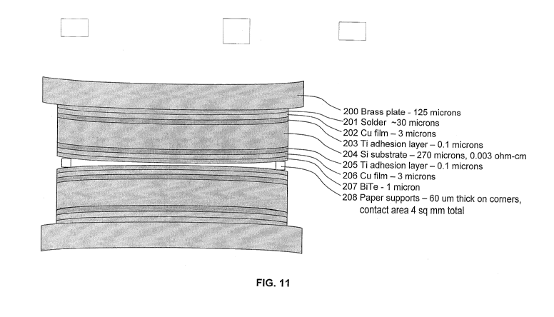
FIG. 11 illustrates an apparatus very similar to FIG. 2a that was built to
test the
concept of this invention. Each electrode was 1 square centimeter. The bimetal
arrangement consisted of a brass plate 200 that was 125 microns thick and was
soldered
to a silicon die 204 that was 270 microns thick. The corner separators 208
were made of
paper 60 microns in thickness and each one consisted of about I square
millimeter of
corner contact area. The thermoelectric layer was formed by depositing 10
nanometers of
Bismuth, followed by 15 nanometers of Tellurium repetitively until the total
thickness of
1 micron was achieved. Copper films 202 and 206 were 3.0 microns thick and
served as
current spreaders, allowing current to be conducted, through the entire area
of the silicon
die 204. Titanium adhesion layers 203 and 205 were placed between the copper
and the
silicon on both top and bottom of silicon die 204. All layers on the silicon
die 204 were
sequentially deposited using thermal evaporation from pure element sources in
an
electron beam evaporation system maintained at high vacuum pressure. After
fabrication,
the finished electrodes were baked at 200 degrees centigrade for about 1 hour
to anneal
the Bi2Te3 film. The bottom electrode was fabricated identically to the top
electrode,
only positioned upside down as shown in FIG. 11.
The entire electrode pair illustrated in FIG. 11 was placed between spring-
loaded
electrical connectors in a vacuum bell jar. A voltage from a DC power supply
was
applied to the spring-loaded connectors. A voltmeter permitted reading the
voltage right
at the brass plates, and two small thermocouples permitted reading the
temperature on
each brass plate. The current flow through the device was read from a meter on
the
power supply.
During the experiment, the applied voltage was increased gradually, and the
voltage, current, and temperature of each electrode were measured at several
data points.
21
CA 02710548 2010-06-22
WO 2009/102706 PCT/US2009/033660
As the supply voltage increased, the current increased, and the electrical
resistance of the
device caused both electrodes to heat up. As the electrode pair heated up to
approximately 50 degrees centigrade, a nanometer gap started to form.
FIG. 12 illustrates that a nanometer gap formed and that the thermoelectric
effect
was enhanced by the formation of the nanometer vacuum gap. In FIG. 12, the
Peltier
coefficient axis 211 was indicated for several readings of the average
electrode
temperature axis 212. The Peltier coefficient is proportional to the Seebeck
coefficient.
As the device heats up to approximately 57 degrees centigrade, the gap begins
to form
and the Peltier coefficient rises rapidly providing evidence of the advantage
of this
invention's gap forming means. The round data points 213 indicate current flow
in the
opposite direction as the square data points 214. The ZT for this experiment
was
estimated to be 0.2.
Many limitations in the apparatus used for these measurements prevented the
demonstration of a ZT that is better than the state of the art ZT of 1.04. The
non-uniform
stoichiometry of the film deposition process caused inferior Peltier and
Seebeck
coefficients prior to gap formation. The expected Peltier coefficient value
for Bi2Te3 is
about 0.06 watts/amp. The value measured in this experiment for without the
gap was
about 0.0 15 watts/amp. The lower measured value is likely due to the non-
uniform
stoichiometry from the alternating layers, as the Peltier coefficient is
strongly dependent
on correct stoichiometry for this material. The surface roughness was much
greater than
the required 1 nanometer. The curvature of the soldered brass plate onto the
silicon die is
much greater than what would be possible with hot-substrate deposition in a
semiconductor foundry. Finally, the paper spacers introduced much greater
thermal
backflow than would the glass separators in the preferred embodiment. The
glass
separators can be fabricated with semiconductor processing to be 25 microns
laterally
instead of the 1000 microns for the paper spacers used in this experiment.
Without these
limitations, a significant improvement over the state of the art ZT would have
been
expected.
Multiples units of this device can be connected together in parallel and in
series
in order to achieve higher levels of energy conversion or to match voltages
with the
power supply or electrical load.
It should be emphasized that the above-described embodiments of the present
device and process, particularly, and "preferred" embodiments, are merely
possible
examples of implementations and merely set forth for a clear understanding of
the
22
CA 02710548 2010-06-22
WO 2009/102706 PCT/US2009/033660
principles of the invention. Many different embodiments of the tunneling and
self-
positioning electrode device described herein may be designed and/or
fabricated without
departing from the spirit and scope of the invention. All such modifications
and
variations are intended to be included herein within the scope of this
disclosure and
protected by the following claims. Therefore the scope of the invention is not
intended
to be limited except as indicated in the appended claims.
23