Note: Descriptions are shown in the official language in which they were submitted.
CA 02710940 2010-06-28
WO 2009/099926 PCT/US2009/032569
RADIO FREQUENCY CONNECTOR
FIELD OF THE INVENTION
[0001] This invention relates to radio frequency (RF) connectors and more
particularly to RF connectors having a relatively high isolation
characteristic.
BACKGROUND OF THE INVENTION
[0002] As is known in the art, a radio frequency (RF) connector is an
electrical
connector designed to work at RF frequencies in the megahertz range and
above. RF connectors are often used with coaxial cables. One desirable
characteristc of an RF connector is its ability to maintain the shielding
provided by a coaxial cable as well as the characteristic of reducing changes
in transmission line impedance at the interface of the coaxial cable and the
RF connector. Mechanically, RF connectors typically utlize a fastening
mechanism (thread, bayonet, braces, push-pull) and springs to provide a low
ohmic electric contact while sparing connector surfaces (which are often gold-
plated). This allows above one-thousand reconnects and reduces the
required insertion force.
[0003] As is also known, research activity in the area of RF circuit design
has
surged in the last decade in direct response to market demand for
inexpensive, high data rate wireless transceivers. Such transceivers and
other circuits utilize connectors so that signals can be coupled between
various modules.
[0004] One type of RF connector is a so-called "edge-launch" connector.
Edge launch connectors are provided having a housing through which a
signal pin is disposed to contact a circuit on a printed wiring board (PWB).
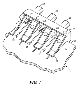
The PWB is often provided as part of a circuit card assembly (CCA), for
example. RF signals propagate through the edge launch connector via the
signal pin. As the name implies, edge launch connectors couple to an edge of
the PWB (and thus, an edge of a CCA). One attractive feature of an edge
launch connector is that owing to the manner in which such connectors are
CA 02710940 2010-06-28
WO 2009/099926 PCT/US2009/032569
coupled to CCAs, edge launch connectors often introduce a relatively small
insertion loss characteristic and a relatively low voltage standing wave ratio
(VSWR) characteristic when connected to circuits on the CCA. One drawback
with edge launch connectors, however, is that it is relatively difficult to
provide a
high degree of isolation between signal pins of multiple edge launch
connectors
mounted in proximity to each other on a CCA.
[0005] This is particularly true when isolation levels of about 100 dB are
required between connectors mounted in proximity to each other on the same
CCA. In one application, for example, an RF module requires over 100 dB of
isolation from individual signals operating at similar microwave frequencies
on a
CCA. A common problem with conventional RF edge launch connectors is RF
leakage which exists between the connector and the circuit card or between the
connector and a circuit card cover due to connector geometry and practical
limitations in holding mechanical tolerances during manufacturing operations.
To improve the isolation characteristic of a conventional edge launch
connector, an EMI gasket is sometimes disposed between the mating surfaces
of the CCA and the connector disposed against the edge of the CCA. One
problem with this gasket approach is that the gasket can become deformed
(e.g. "bunch up") or can shear off completely resulting in gaps between the
connector and CCA surfaces. This reduces the isolation characteristic of the
connector.
[0006] It would, therefore, be desirable to provide an RF connector which can
provide a high level of signal isolation between connector signal pins when
several such signal pins are disposed in proximity on a CCA. It would also be
desirable to provide an RF connector which can blindly mate to a circuit card
since this provides for ease of circuit card insertion/extraction. It would
also be
desirable to provide an RF connector which can be mounted in close proximity
with other connectors to accommodate tightly spaced signal paths necessitated
by electrical and mechanical design constraints on a circuit. It would also be
desirable to provide an edge launch RF connector which has one or more of
the afore-mentioned characteristics.
2
CA 02710940 2010-06-28
WO 2009/099926 PCT/US2009/032569
SUMMARY OF THE INVENTION
[0007] In accordance with the concepts and structures described herein, an
edge launch RF connector assembly adapted to couple to a printed wiring
board (PWB) of a circuit card assembly (CCA) includes an RF connector
block having a plurality of dividers projecting from a surface of the
connector
block, an EMI gasket configured to interface with the dividers of the RF
connector block and the circuit card and a cover adapted to be disposed over
the sloped surface of the RF connector block and a plurality of signal
contacts
with at least one divider disposed between each signal contact..
[0008] With this particular arrangement, an edge launch RF connector
assembly having a high degree of isolation between signal contacts is
provided. In one particular embodiment, the RF connector block includes a
body portion having a slot provided therein to accept an edge of the PWB to
which the RF connector block be will coupled and the dividers projecting from
the body portion and having a sloped surface. The plurality of signal contacts
also project from a first surface of the body portion and a plurality of
ground
tabs project from the first surface of the body portion proximate the signal
contacts with the plurality of ground tabs adapted to couple a ground plane of
the PWB to the RF connector block.
[0009] In one particular embodiment, the sloped dividers have one surface
having a twenty-five degree sloping geometry (with the angle being measured
relative to and from a PWB surface which contacts the divider). This allows
the RF gasket to be provided as one continuous RF gasket to be disposed
between the RF connector block and the cover with no gaps therebetween. In
this manner, the signal contacts in the RF connector block are isolated from
each other and are also isolated from noise outside the RF module to which
the connector assembly is coupled. Thus, the edge launch RF connector
assembly isolates each individual signal from each other and from extraneous
RF signals external to the PWB (e.g. RF noise signals). Furthermore, each
divider in the assembly includes an insert disposed between each signal
3
CA 02710940 2010-06-28
WO 2009/099926 PCT/US2009/032569
contact. The insert allows the circuit card ground plane to be securely mated
to the connector. Providing a secure connection between grounded portions
of the connector and the RFP WB ground plane can improve the connector
isolation characteristic as well as other connector performance
characteristics
such as insertion loss and impedance matching characteristics.
[0010] In one embodiment, there are two ground tabs on both sides of each
signal pin. The ground tabs are coupled to a ground plane of the PWB to
further improve the signal integrity and maintain a relatively high degree of
isolation between signal contacts. By tightly grouping a plurality of signal
contacts into one connector body, this approach also reduces the amount of
circuit card space needed for RF connections. In one embodiment, two such
edge launch RF connector assemblies, each containing seven edge launch
connectors, fit on the edge of a standard 6U VME CCA, thereby allowing
fourteen isolated RF signals to enter and exit the CCA.
[0011] The "dividers" are also sometimes referred to herein as "fingers" or
"signal isolators." The angle (or slope) of one divider surface is selected to
match the angle of the PWB on which it is disposed. A second surface of the
divider is sloped. In one embodiment, the angle (or slope) of the second
divider surface can range from about 10 to about 40 degrees as measured
relative to and taken from a PWB surface upon which a connector signal
contact is disposed. Factors to consider in selecting a specific angle for the
sloped divider surface include, but are not limited to the particular type of
material from which a gasket (e.g. an EMI gasket) disposed over the dividers
is provided as well as the frequency range over which the connectors must
operate. In one embodiment, twenty- five degrees is preferred. The smaller
the angle chosen for the sloped surface, then the longer the divider which
leaves less room for components on the PWB. If a larger angle is used,
however, the divider becomes shorter using less component space, but there
is an increase in the risk of shearing or bunching a gasket disposed over the
sloped surface of the divider. A tear or other imperfection or bunching of the
gasket would lead to a significant decrease in isolation between signal
4
CA 02710940 2010-06-28
WO 2009/099926 PCT/US2009/032569
contacts. Thus, the designer needs to choose the angle that best fits the
amount of PWB space available and matches the gasket material used. The
dividers may be provided having a truncated-right triangle cross-sectional
shape (in a cross-section taken along a central-longitudinal axis of the
divider). It should be appreciated, of course, that other shapes may also be
used including but not limited to: curved shapes; irregular shapes or regular
shapes generally composed, in whole or in part, of straight line segments; and
irregular shapes or regular shapes generally composed, in whole or in part, of
arc segments.
[0012] In accordance with a further aspect of the concepts described herein,
an RF connector block includes a body portion having a slot provided therein
to accept an edge of a PWB to which the RF connector block will coupled, a
plurality of sloped dividers projecting from a surface of the body portion, a
plurality of signal contacts projecting a first surface of the body portion
and a
plurality of ground tabs projecting from the first surface of the body portion
proximate the signal contacts wherein the plurality of ground tabs are adapted
to couple a ground plane of the PWB to which the RF connector block will be
coupled.
[0013] With this particular arrangement, an RF connector block, which
provides a high level of RF isolation between signal paths on a CCA is
provided. By providing the dividers having sloped surfaces (e.g. in the range
of about twenty-five degrees to about forty-five degrees with respect to the
PWB surface), a continuous bead of EMI gasket can be placed on a CCA
cover and will not shear off when the cover is disposed over the gasket and is
sealed to the connector block surface. Furthermore, the connector block can
be provided with guide pins to ensure proper alignment of signal contacts to
signal paths on a PWB to thereby reduce signal loss. When the connector
block is provided a having a groove therein (via milling or some other
technique), the edge of a circuit card can seat into the grove thereby
improving isolation between the top and bottom surfaces of the card. In other
embodiments, the PWB or CCA may be provided having a slot, groove, or
5
CA 02710940 2010-06-28
WO 2009/099926 PCT/US2009/032569
other feature which mates with a corresponding feature on the connector
block or some other portion of the connector assembly. By providing the
connector with threaded inserts between each signal contact, a screw or other
fastener is allowed to come through the bottom of the circuit and securely
fasten the connector block onto a ground plane of the card which improves
isolation between signal contacts (e.g. pin-to-pin isolation). Furthermore, by
providing the ground tabs as solderable ground tabs in close proximity to both
sides of each signal contact, the connector block provides improved
grounding and impedance matching (e.g. VSWR characteristics) to RF
connectors coupled to the connector block.
BRIEF DESCRIPTION OF THE DRAWINGS
[0014] The foregoing features of this invention, as well as the invention
itself,
may be more fully understood from the following description of the drawings in
which:
[0015] FIG. 1 is an isometric top view of a portion of a radio frequency (RF)
connector block coupled to an RF;
[0016] FIG. 2 is an exploded isometric top view of a portion of an RF
connector block and an RF printed wiring board (PWB);
[0017] FIG. 3 is an exploded isometric bottom view of an RF connector block
and an RF PWB;
[0018] FIG. 4 is an isometric top view of a portion of an RF connector block
assembled on an RF PWB;
[0019] FIG. 4A is a side view of an RF connector block and top RF cover
assembled on an RF PWB;
[0020] FIG. 5 is a top view of an RF connector block;
6
CA 02710940 2010-06-28
WO 2009/099926 PCT/US2009/032569
[0021] FIG. 5A is a front view of an RF connector block;
[0022] FIG. 5B is a bottom view of an RF connector block; and
[0023] FIG. 5C is a side view of an RF connector block.
[0024] FIG. 6 is a side sectional view of an RF connector block;
[0025] FIG. 7 is an exploded isometric view of an RF connector block
assembled into an RF CCA module;
[0026] FIG. 7A is an isometric view of an RF connector block assembled into
an RF CCA module;
[0027] FIG. 8 is a top view of an RF PWB having cut-outs made therein to
accept an RF connector block;
[0028] FIG. 8A is a top view of an RF connector block assembled to an RF
PWB;
[0029] FIG. 8B is a bottom view of an RF connector block assembled to an
RF PWB;
DETAILED DESCRIPTION OF THE PREFERRED EMBODIMENTS
[0030] Referring now to FIGs. 1 - 4A in which like elements are provided
having like reference designations throughout the several views, an edge
launch radio frequency (RF) connector block 10 is coupled to an edge 12a of
a printed wiring board (PWB) 12 having first and second opposing surfaces
13a, 13b. The RF connector block 10 includes a body portion 14 having a
plurality of threaded holes 15 provided therein. In one embodiment, holes 15
are provided from threaded #2 inserts. As is known, a "threaded insert" is a
piece of hardware which would be inserted into hole 15 to make it a threaded
7
CA 02710940 2010-06-28
WO 2009/099926 PCT/US2009/032569
hole instead of a thru hole. This is done instead of mechanically threading
hole 15. As will become apparent from the description hereinbelow in
conjunction with FIG. 7, threaded inserts 15 are used to secure an RF cover
to the RF connector which improves isolation between different RF signals.
[0031] A plurality of dividers 16 project from a surface of body portion 14.
The dividers 16 have a first or lower surface disposed on a first or top
surface
13a of the PWB 12 and a second or upper sloped surface 17. An optional
hole 42 is provided in dividers 16. In one embodiment, and for reasons which
will become apparent from the description herein below, hole 42 is provided
as a threaded hole which accepts a screw which secures the connector to
PWB 12. In one embodiment, stainless steel threaded inserts are disposed in
openings provided the connector block. Thus, in the event that screws 40
used to attach a connector to a circuit card are provided from a relatively
hard
material (e.g. steel or . stainless steel) and the connector block is provided
from a material which is softer than the screw material (e.g. aluminum is
softer
than stainless steel), then the screws 40 will not damage softer connector
block material.
[0032] As can be most clearly seen in FIGs. 2 and 3, the body portion 14 has
an opening 18, (such as a slot, a channel, or a groove) provided therein.
Opening 18 is provided having a shape which can accept at least a portion of
PWB 12 such as edge 12a of the PWB 12. Also projecting from a surface of
body portion 14 of connector block 10 are a plurality of signal contacts 20
(e.g. pins, tabs or the like) as well as ground contacts 24. On the PWB side,
the signal contacts lead to signal paths 21 on the PWB. Signal paths 21 may
be implemented as any type of RF transmission line including but not limited
to any type of printed circuit transmission line including but not limited to
stripline, microstrip, and co-planar waveguide.
[0033] It should be appreciated that slight modifications may need to be
made in connector 10 depending upon the manner in which the signal paths
are implemented. It should also be understood that such changes are within
8
CA 02710940 2010-06-28
WO 2009/099926 PCT/US2009/032569
the level of skill of one of ordinary skill in the art and that such changes
do not
depart from the concepts described herein which relate to an RF connector
which provides a high RF isolation characteristic between proximately
disposed signal contacts.
[0034] To promote clarity in the drawings, signal paths 21 have been omitted
from drawing FIG. 2, but can be clearly seen in FIG. 4. The other end of
signal contacts 20 (i.e. the portions of signal contacts 20 which are not
visible
in FIGs. 1-4) lead to a connector mating structure 22. Also projecting from a
surface of the body portion 14 are a plurality of ground tabs 24, which are
coupled to a ground plane of the PWB. In one embodiment, a pair of ground
tabs are provided on each side of every signal contact 20.
[0035] As may be most clearly seen in FIGs. 4 and 4A, on the PWB side of
the connector block, the signal contact 20 are coupled to respective ones of
signal paths 21 on the PWB (signal paths 21 being omitted from Fig. 1 to
improve the clarity of the figure) and the ground tabs 24 are coupled to the
ground plane of the PWB. Each of the signal contacts are adapted to couple
RF signals through the connector block and to an RF connector coupled to
the opposite side of the connector block 14.
[0036] In one embodiment, the ground tabs are milled into body portion 14 of
the connector block 10. Thus, in this embodiment, the connector block and
ground tabs are provided from a monolithic block. Also, in one embodiment,
the ground tabs are coupled to the ground plane of the PWB by soldering the
ground tabs to the ground plane. Techniques other than soldering may, of
course, also be used to couple the ground tabs to the PWB ground plane. It
should, of course, also be appreciated that in other embodiments, it may be
preferable, desirable or even necessary to provide the ground tabs as a part
which is separate from the body portion (or some other portion) of the
connector block in which case the ground tabs would be secured to the
connector block by an appropriate technique (e.g. by boring one or more
holes into a portion of the connector block and press fitting the ground tabs
9
CA 02710940 2010-06-28
WO 2009/099926 PCT/US2009/032569
into the one or more holes or by otherwise securing the ground tabs to the
connector block via fasteners, epoxy, glue or via some other technique).
[0037] As may also be most clearly seen in FIGs. 4 and 4A, an RF gasket 19
is disposed over the sloped dividers 16 to help provide the RF connector
block having a relatively high isolation characteristic between RF signals
propagation on each of the signal contacts 20. Thus, for example, RF signals
propagating on a first signal contact 20a are highly isolated from RF signals
propagating on signal contacts 20b, 20c. In one embodiment, RF gasket 19
may be provided as a continuous EMI gasket which increases signal isolation
between signal contacts 20. Also, in one embodiment, 110 db of isolation is
provided between signal contacts. It should , of course, be appreciated that
the specific amount of isolation achieved in any particular embodiment is
highly dependent upon the type of RF connector used within connector block
10 as well as the operational frequency range of the connector.
[0038] Referring now to FIG. 4A, a top RF cover 30 is secured to connector
block 10 via screws (not shown in FIG. 4A) which pass through cover 30 and
mate with openings 15 in the RF connector block. A bottom cover 31 is
secured to PWB 12 and connector block 10 via screws 40 (only one of which
is visible in FIG. 4A) which mates with a threaded hole provided in RF
connector block 10 (e.g. threaded hole 42 in FIG. 3).
[0039] It should be noted that EMI gasket 19 is disposed over sloped surface
17. It should be appreciated that surface 17 is provided having a gradual
slope selected to reduce shear force that could tear or bunch the EMI gasket
19.
[0040] In one embodiment, opening or slot 18 in connector block can accept
any PWB edge having a thickness less than .112 inches and the angle of the
slope on the sloped dividers 16 can range from about 10 to about 40 degrees
as measured from PWB surface 13a with a slope of about 25 degrees being
preferred. The particular angle of the sloped divider surface to use in any
CA 02710940 2010-06-28
WO 2009/099926 PCT/US2009/032569
particular application is selected in accordance with a variety of factors
including, but not limited to, the type of material from which the gasket 19
is
provided and the amount of available space on the PWB. The smaller the
angle chosen, the longer the divider which leaves less room for components
on the PWB. The larger the angle used, the shorter the length of the divider
thereby using less space on the PWB (which leaves more space on the PWB,
e.g. for mounting circuit components), but the risk of shearing or bunching
the
gasket 19 on top of the divider 16 increases. If the gasket shears or bunches,
this would likely lead to a decrease (possibly a significant decrease) in the
RF
isolation characteristic between RF signals propagating on adjacent or even
proximate signal paths and/or signal contacts. Thus, an angle that best fits
the amount of PWB space available and matches the gasket material should
be used. It should be appreciated that the slope of surface 17 has a
relationship to the shear force exerted with cover 30 disposed over gasket 17
and that such sheer force could tear or bunch the gasket 19. In particular,
the
more shallow the slope of surface 17, the lower the shear force.
[0041] As shown in FIG. 4A, a top cover 30 is disposed over the connector
block 10 and the RF PWB 12 to further improve the isolation characteristic
between the signal pins 20. By sealing the RF cover 30 to the RF PWB 12, a
high level of RF isolation between signal contacts coupled to the PWB 12 is
provided.
[0042] Referring now to FIG. 2, in one embodiment PWB 12 is provided
having one or more slots therein. In some embodiments, slot(s) 92 may be
provided as a plated slot(s) 92 (also visible in FIG. 8). Slots 92 accept a
corresponding tab 46 (FIG. 3) projecting from a surface of the RF connector
block 18. In the embodiment shown in FIG. 3, tabs 46 project from a surface
of channel 18. The slots 92 and mating tabs 46 cooperate to align the
connector 10 and PWB 12 in desired relative positions.
[0043] The PWB 12 also has a plurality of through holes 44 provided therein.
Through holes 44 accept connector mounting screws 40 (FIG. 3) which are
11
CA 02710940 2010-06-28
WO 2009/099926 PCT/US2009/032569
disposed through openings 42 (FIG. 3) in dividers 16. The screws 40 secure
the PWB 12 to the RF connector 10. In the embodiment shown herein,
screws 44 are located on both sides of signal contacts 20 (and hence on both
sides of an RF signal path leading to contacts 20) which improves RF
isolation between RF signals propagating along the multiple signal paths to
the respective signal contacts 20. In one embodiment, openings 42 are
provided as threaded openings sized to accept a #2 size screw 40 which is
used to secure the connector 10 to the PWB 12 The fastener 40 travels
through bottom cover 31, board hole 44, then into connector hole 42. In some
embodiments a lock-washer may be used on surface 13b to keep the fastener
from pulling out.
[0044] In one embodiment, the ground tabs 24 are soldered to a surface 12a
of PWB 12. This improves isolation between RF signals propagating through
signal contacts 20. The signal contacts are soldered to the signal paths 21
(FIG. 4) on PWB 12.
[0045] In the embodiment described herein, the PWB solder layout is
provided in a manner which matches industry standard SMP edge mount
connectors. It should, however, be appreciated that other configurations may
also be used to match other industry standard connectors or configurations
may be used to match any type of standard or non-standard connectors.
Thus, connector 10 may be configured for use in a wide variety of applications
requiring a large number of different connector types including, but not
limited
to SMA, SSMA, ETC. SMB, SSMB and SMP connector types.
[0046] Connector block surfacel4 also has provided therein a plurality of
holes 15. In one embodiment, holes 15 may be provided as threaded #2
inserts which are configured to secure an RF cover (e.g. RF cover 30 in FIG.
4A) to the RF connector block10 which improves isolation between different
RF signals propagating on PWB 12.
12
CA 02710940 2010-06-28
WO 2009/099926 PCT/US2009/032569
[0047] As shown in FIG 3., screws 40 are disposed in holes 42 in the
dividers 16 and through holes 44 in the PWB. The screws secure the PWB to
the RF connector block, while at the same time improving the RF isolation
between the signal contacts. The opening 18 has tabs 46 projecting
therefrom, which mate with corresponding openings 48 in the PWB.
[0048] By providing the connector assembly having the mounting tabs and
screws, the RF connector block 10 is adapted to blindly mate to a circuit card
assembly (CCA) having corresponding mating structures (e.g. openings 44,
48).
[0049] In one embodiment, screws 40 are provided as #2 Phillips-head
screws which are disposed through openings in both bottom cover 31 (FIB.
4A) and RFPWB 12 in divider 16. Those of ordinary skill in the art will, of
course, understand how to select the size (e.g. diameter, length, thread
pitch,
etc. ...) of screws 40 for particular applications. It should be understood
that
the size of screws 40 and openings 42, 44 are selected to cooperate with
each other.
[0050] As noted above, an edge of PWB 12a fits into groove 18 on connector
10. In some embodiments, groove 18 can be soldered or sealed into the
PWB to improve isolation. This solder connection in groove 18 is made
between the surface of PWB edge 12a and surface 18a of groove 18. In one
embodiment, PWB slots 48 are plated and are soldered to isolation tabs 46 on
connector 10.
[0051] Referring now to FIGs. 5-5C in which like elements are provided
having like reference designations throughout the several views, an RF
connector block 50 able to accept seven RF connectors are shown. It should
be appreciated that although seven connectors are shown, the connector
block may, of course, be provided having fewer or greater than seven
connectors.
13
CA 02710940 2010-06-28
WO 2009/099926 PCT/US2009/032569
[0052] With seven connectors, the connector block 50 may be secured to a
PWB with four screws, disposed through openings 52 arranged approximately
as shown The particular number of screws to use in any application is
selected to help provide a desired amount of isolation between signal
contacts. Also, the connector block may be secured to the PWB via a solder
technique or any other technique known to those of ordinary skill in the art.
[0053] Referring now to FIG. 6, a partial side-sectional view of RF connector
block 150 reveals openings 67, which may be used to mount an RF connector
(not shown) or an RF backplane (not shown) to the connector block.
[0054] Referring now to FIGs. 7 and 7A, in which like elements are provided
having like reference designations throughout the several views, a pair of RF
connector assemblies 70a, 70b are coupled to a circuit card assembly (CCA}
module 72 provided from an RF CCA 76 and an RF CCA cover 82. Each RF
connector assembly 70a, 70b includes an RF connector block 74 coupled
to an RF CCA 76, an RF connector backplane 78 which serves to secure and
align the connectors 80 which couple to the connector block 74, , a plurality
of
RF connector receptacles 80 coupled to the RF connector block through the
backplane and a cover 82. In this particular embodiment, the cover 82 serves
as both a cover for the RF connector block as well as a top cover for the RF
CCA. In some embodiments, the cover for the RF connector assembly may
be provided having a size and shape which covers the RF connector block. In
this case, CCA module would be provided having a top and a bottom cover
84. It should be appreciated that the decision to use a cover in a particular
application depends upon the application and it not necessarily related to the
connector or improving isolation between connector contacts.
[0055] Referring now to FIGs. 8-8B in which like elements are provided
having like reference designations throughout the several views, a PWB 90
has a first plurality of cut-outs 92 provided in an edge thereof. The cut-outs
92 are provided to accept a like plurality of tabs 93 (which may be the same
as or similar to tabs 46 in Fig. 3) provided on the RF connector block. With
this technique, the RF connector block can be properly aligned on the PWB
90. This also allows blind mating of the RF connector block to the PWB. The
14
CA 02710940 2010-06-28
WO 2009/099926 PCT/US2009/032569
PWB also includes holes 94, which accept mounting screws 95 (which may
be the same as or similar to screw 40 shown in Fig. 3).
[0056] Furthermore the connector assembly described herein includes guide
pins to ensure proper signal alignment and reduce loss; this connector has a
groove milled into it that allows the edge of the circuit card to seal into
improving isolation from the topside of the card to the bottom; this connector
has threaded inserts between each signal to allow a screw to come through
the bottom of the circuit and securely fasten the connector into the cards top
ground plane, improving pin-to-pin isolation; and for additional grounding and
improved VSWR, solderable ground tabs have been added very closely to
both sides of each signal pin.
[0057] What is claimed is: