Note: Descriptions are shown in the official language in which they were submitted.
CA 02710948 2010-06-28
WO 2009/085660 PCT/US2008/086590
MAGNETIC SHIELDING GASKET AND METHOD OF FILLING A GAP IN AN
EMI SHIELDED SYSTEM
Field of the Invention
The present invention relates to an electromagnetic shield technology,
particularly, to
a magnetic shielding gasket for shielding the Electro Magnetic Interference
(EMI)/Radio
Frequency Interference (RFI). In addition, the present invention also relates
to a method of
filling a gap in an EMI shielded system.
Background
Electro Magnetic Interference (EMI) is an undesired electromagnetism generated
in
or radiated from an electronic/electric apparatus, which may disadvantageously
affect the
normal operations of the electronic/electric apparatus. Generally, such
Electro Magnetic
Interference may occur at any frequency band of the electromagnetic frequency
spectrum.
Furthermore, Radio Frequency Interference (RFI) often occurs accompanying with
Electro
Magnetic Interference (EMI). In practice, Radio Frequency Interference (RFI)
is controlled
to happen at the Radio Frequency of the electromagnetic frequency spectrum,
that is, at a
frequency band from 10 KHz to 100 GHz.
In order to effectively prevent Electro Magnetic Interference (EMI)/Radio
Frequency
Interference (RFI), generally, a shield is disposed between the source of
EMI/RFI and the
region to be protected. The shield is used for preventing the electromagnetic
energy from
being radiated out of the source of EMI/RFI, and also for preventing the outer
electromagnetic energy from entering into the source of EMI/RFI.
Commonly, the shield is formed in a conductive seal shell that may be grounded
via a
ground wire on PCB. In prior art, the conductive seal shell may be integrally
made of a
magnetic shielding gasket material. In addition, in practice, according to the
requirement
from the inner circuit or structure, a groove may be provided in the
conductive seal shell so
-1-
CA 02710948 2010-06-28
WO 2009/085660 PCT/US2008/086590
as to form a gap in the shield. In this case, the gap formed in the shield may
be filled with a
shielding gasket so as to prevent the electromagnetic energy from being
radiated out of the
source of EMI/RFI, and also to prevent the outer electromagnetic energy from
entering
into the electronic/electric apparatus.
Recently, the electronic/electric apparatuses, such as mobile telephone, PDA,
and
navigation system, are becoming more compact and with better portability. On
the one
hand, in order to prevent the dust or moisture from entering into the core
parts, such as
LCD modules, of these communication equipments, and to prevent the impaction
and
vibration to the core parts due to bump or fall during carrying or delivering,
it is needed to
provide an absorption gasket material with high impact and vibration
absorptivity outside
these electronic modules of the electronic/electric apparatus. Such absorption
gasket
material generally is made of an open-celled material, such as polyurethane
foam, so that
the absorption gasket material has certain resilience and recoverability. On
the other hand,
since the LCD modules of these electronic communication equipments are
required to
have larger screen and multi-functions such as character or picture
communication
function, and photographing function, the circuits and electronic modules in
the
electronic/electric apparatus become sensitive to the exterior static
electricity,
electromagnetic wave, and magnetic field, and tend to be disadvantageously
affected by
the inner and outer sources of Electro Magnetic Interference/Radio Frequency
Interference.
Thus, not only the absorption gasket material of aforesaid electronic/electric
apparatus need have a high impact and vibration absorptivity, but also have a
gapless seal
capability in a narrow space of the electronic/electric apparatus and a good
shielding
capability to Electro Magnetic Interference (EMI)/Radio Frequency Interference
(RFI)
generated in or outside the electronic/electric apparatus.
US 6,309,742 discloses a magnetic shielding gasket formed by depositing a
metal
coating onto an open-celled foam structure such as a silicone rubber. Since
the deposited
metal material penetrates the open-celled foam structure so that the open-
celled foam
structure has an excellent conductivity. Accordingly, the gasket material is
die-cut into or
cut into various shapes or shaped into a shielding structure, and then filled
in or covered
-2-
CA 02710948 2010-06-28
WO 2009/085660 PCT/US2008/086590
around the electronic/electric apparatus so as to shield Electro Magnetic
Interference
(EMI)/Radio Frequency Interference (RFI) generated in or outside the
electronic/electric
apparatus by means of its conductivity.
However, the above-mentioned prior art has following disadvantages. Firstly,
although the gasket material of prior art has certain conductivity and has
good shielding
effect on the static electricity and magnetic field, the gasket material has
poor shielding
effect on the magnetic field generated in or outside the electronic/electric
apparatus,
particularly, on the near field magnetic field. Secondly, although the gasket
material of
prior art has good resilience and recoverability, the mechanical strength of
gasket material
is very low for it is only formed of the open-celled foam structure,
increasing the difficulty
in cutting or die-cutting out the gasket material to predetermined shape and
also increasing
difficulty of performing the cutting or die-cutting operation. Also, it is
very difficult to
locate the gasket material on the predetermined electronic module of the
electronic/electric
apparatus.
Summary
The present inventors have determined that it is desirable to provide a
magnetic
shielding gasket that not only can effectively shield the electric field and
magnetic field,
but also has sufficient resilience, recoverability and mechanical strength so
as to obtain an
excellent sealing performance while improving the operability during cutting
and locating
the gasket material and the efficiency during machining and assembling.
The present invention is directed to solve at least one aspect of the
aforesaid problems
existing in the prior art.
One aspect of the present invention is to provide a magnetic shielding gasket
having
magnetic permeability, which can effectively shield the electric field and has
a satisfactory
magnetic field shielding performance.
Another aspect of the present invention is to provide a magnetic shielding
gasket
comprising a structure reinforcing layer to achieve a satisfied mechanical
strength, thereby
-3-
CA 02710948 2010-06-28
WO 2009/085660 PCT/US2008/086590
improving the operability during cutting and locating the gasket material and
the efficiency
during machining and assembling.
Another aspect of the present invention is to provide a method of filling a
gap in an
EMI shielded system with aforesaid magnetic shielding gasket material.
One embodiment of the present invention is to provide a magnetic shielding
gasket,
comprising: a conductive foam substrate exhibiting resilience and
recoverability and
having a first surface; a magnetic layer attached to said first surface of the
conductive foam
substrate and wherein the magnetic layer exhibits magnetic permeability,
wherein the
initial magnetic permeability of the magnetic layer is greater than 1000 @
0.1A/m and the
maximum magnetic permeability of the magnetic layer is greater than 5000 @
0.1A/m.
Another embodiment of the present invention is to provide a magnetic shielding
gasket, comprising: a conductive foam substrate exhibiting resilience and
recoverability
and having a surface; a structure reinforcing layer made of conductive fabric,
said structure
reinforcing layer being attached to said surface of the conductive foam
substrate; and a
magnetic layer attached to an outer surface of the structure reinforcing layer
and wherein
the magnetic layer exhibits high magnetic permeability, wherein the initial
magnetic
permeability of the magnetic layer is greater than 1000 @ 0.1 A/m and the
maximum
magnetic permeability of the magnetic layer is greater than 5000 @ 0.1A/m. In
one
preferred embodiment, the initial magnetic permeability of the magnetic layer
is greater
than 35,000 @ 0.1A/rn and the maximum magnetic permeability of the magnetic
layer is
greater than 200,000@ 0.1 A/m.
In another preferred embodiment, the initial magnetic permeability of the
magnetic
layer is greater than 50,000 @ 0.1A/m and the maximum magnetic permeability of
the
magnetic layer is greater than 300,000@ 0.1A/m.
In another preferred embodiment, the initial magnetic permeability of the
magnetic
layer is greater than 80,000 @ 0.1A/m and the maximum magnetic permeability of
the
magnetic layer is greater than 400,000@ 0.1A/m.
-4-
CA 02710948 2010-06-28
WO 2009/085660 PCT/US2008/086590
In a further preferred embodiment, the conductive foam substrate further
includes a
second surface opposite to said first surface; and a structure reinforcing
layer made of
conductive fabric is attached to said second surface of the conductive foam
substrate.
In an alternative embodiment, the magnetic shielding gasket further comprises
a
structure reinforcing layer made of conductive fabric, said structure
reinforcing layer being
attached to an outer surface of said magnetic layer.
With the magnetic shielding gasket, the present invention can effectively
shield the
electric field and magnetic field, particularly, the near field magnetic
field. Meanwhile,
since it has appropriate resilience, recoverability and mechanical strength,
the magnetic
shielding gasket can obtain an excellent sealing performance while improving
the
operability during cutting and locating the gasket material, and the
efficiency during
machining and assembling.
Brief Description of the Drawings
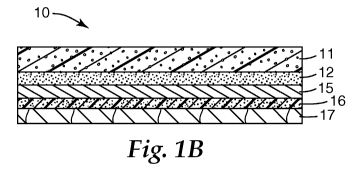
Fig. 1 is a view showing the structure of the magnetic shielding gasket
according to
an embodiment of the present invention, wherein in Fig.1A is a perspective
view
illustrating the construction of the magnetic shielding gasket, and Fig.1B is
a cross-
sectional view of the magnetic shielding gasket.
Fig. 2 is a view showing the structure of the magnetic shielding gasket
according to
another embodiment of the present invention;
Fig. 3 is a view showing the structure of the magnetic shielding gasket
according to a
further embodiment of the present invention;
Fig. 4 is a view showing the structure of the magnetic shielding gasket
according to a
further another embodiment of the present invention;
Fig. 5 is an illustration showing the shielding effect of seal structure of
the magnetic
shielding gasket according to the present invention;
Fig. 6 is a contrastive illustration showing the shielding effect of the
magnetic
shielding gasket of the present invention applied on the Printed Circuit Board
(PCB),
wherein Fig. 6A is an illustration showing the shielding effect of the Printed
Circuit Board
-5-
CA 02710948 2010-06-28
WO 2009/085660 PCT/US2008/086590
(PCB) on which no magnetic shielding gasket is mounted; Fig. 6B is an
illustration
showing the shielding effect of the Printed Circuit Board (PCB) on which the
magnetic
shielding gasket is mounted;
Fig. 7 is a graph showing the experiment data of the shielding effect of the
magnetic
shielding gasket according to the present invention.
Fig. 8 is a graph illustrating hysteresis loop of the magnetic layer according
to an
embodiment of the present invention.
Fig. 9 is schematic view of a typical application of the magnetic shielding
gasket
according to the present invention.
Detailed Description
Preferred embodiments of the present invention will be described hereinafter
in detail
with reference to the attached drawings, wherein the like reference numerals
refer to the
like elements throughout the specification. The present invention may,
however, be
embodied in many different forms and should not be construed as being limited
to the
embodiment set forth herein; rather, this embodiment is provided so that the
present
disclosure will be thorough and complete, and will fully convey the concept of
the
invention to those skilled in the art.
Embodiment 1
Fig.1 is a view showing the structure of the magnetic shielding gasket
according to
an embodiment of the present invention. As shown in Fig. 1, the magnetic
shielding gasket
10 includes a conductive foam substrate 11 and a magnetic layer 15 attached to
the
conductive foam substrate 11. In this embodiment, the conductive foam
substrate 11 is
made of a material having resilience and recoverability and has an upper
surface and a
lower surface (for simplification, the surface on upper side of the drawing is
defined as the
upper surface; the surface on lower side of the drawing is defined as the
lower surface,
referring to the same hereinafter). The magnetic layer 15 is attached to one
surface, for
example, the lower surface shown in Fig. 1, of the conductive foam substrate
11. The
-6-
CA 02710948 2010-06-28
WO 2009/085660 PCT/US2008/086590
magnetic layer 15 exhibits magnetic permeability, wherein the initial magnetic
permeability of the magnetic layer 15 is greater than 1000 @ 0.1A/m and the
maximum
magnetic permeability of the magnetic layer 15 is greater than 5000 @ 0.1A/m.
In an embodiment, the conductive foam substrate 11 is an open-celled foam that
is
made of a resilient macromolecule material, such as polyurethane, by the
expanding or
foaming process and has good resilience. The conductive foam substrate 11,
however, is
not limited to above material, it may be made of any one resilient material
that has
predetermined recoverability upon an external force is applied, for example,
it may be
macromolecule synthetic resin foam such as polyurethane, polyvinyl chloride
(PVC),
silicone, ethylene-vinyl-acetate copolymer (EVA) bend, and polyethylene etc.
On the one hand, for having good impaction absorptivity and anti-vibration,
and for
achieving an excellent sealing performance during pressing the magnetic
shielding gasket
10 into the predetermined gap, the conductive foam substrate 11 should exhibit
compressibility during an external force is applied thereon.
On the other hand, the conductive foam substrate 11 also should exhibit
suitable
recoverability when the external force is removed. In an embodiment, the
magnetic
shielding gasket 10 having aforesaid conductive foam substrate 11 is
substantially
deformable with less than 50 psi of pressure and substantially recoverable
after the
pressure is removed. Further, after the pressure is removed, the gasket 10 is
able to recover
at least 10% of the amount it is compressed. In a preferred embodiment, after
the pressure
is removed, the gasketl0 is able to recover at least 30% of the amount it is
compressed. In
a preferred embodiment, after the pressure is removed, the gasket 10 is able
to recover at
least 70% of the amount it is compressed.
The open-celled foam structure has a pore density of 50-250ppi, preferably 60-
150ppi,
and more preferably 80-120ppi. In order to have good conductivity, the
conductive foam
substrate 11 is formed by depositing a metal coating onto the open-celled foam
structure
via a vacuum evaporation coating process, an electroplating process or
chemical plating
process. Since the open-celled foam structure has a plurality of pores, after
depositing a
metal coating onto the open-celled foam structure, the conductive foam
substrate 11 is not
-7-
CA 02710948 2010-06-28
WO 2009/085660 PCT/US2008/086590
only conductive on the surface thereof, but also conductive in vertical
direction and other
directions thereof, so as to form a continuously conductive open-celled foam
structure in
three-dimensions.
The method for depositing a metal coating onto the conductive foam substrate
11 may
includes at least one of the vacuum evaporation coating process,
electroplating process or
chemical plating process. The metal coating comprises at least one of Cu, Ni,
Sn, Au, Ag,
Co and Pd and the mixture thereof. In one embodiment, the metal coating may be
Ni-
coating + Cu-coating + Ni-coating, Ni-vacuum evaporation coating + Ni-
electroplating,
chemical catalyst coating + Cu-chemical plating + Ni-electroplating, Ni-
coating + Cu-
coating + Sn-coating, chemical catalyst coating + Cu-chemical plating + Sn-
electroplating.
The metal coating deposited onto the conductive foam substrate 11 has a
thickness of
0.5-10mm, preferably 1.0-3.0mm, more preferably 1.5-2.0mm.
In one preferred embodiment, the conductive foam substrate 11 has a thickness
of
1.6mm and a pore density of 1 l Oppi. Using Ni-vacuum evaporation coating
process + Ni-
electroplating process, the metal coating is deposited onto the conductive
foam substrate
11. The Ni-vacuum evaporation coating has an average thickness less than 0.01
mm and a
density of 0.3-0.4 g/m2, and the Ni-electroplating has an average thickness
equal to 1 mm
and a density of 15-20 g/m2.
The magnetic layer 15 may be made of at least one high permeability alloy
ribbon of
the group consisting of permalloy ribbon, nanocrystalline iron-based alloy
ribbon, and Co-
based amorphous alloy ribbon. The magnetic layer 15 having aforesaid material
exhibits
excellent conductivity and high magnetic permeability. Accordingly, the
initial magnetic
permeability of the magnetic layer 15 is greater than 1000 @ O.lA/m and the
maximum
magnetic permeability of the magnetic layer 15 is greater than 5000 @ O.1A/m.
With the
above high value of magnetic permeability of the magnetic layer 15, the
magnetic field of
the EMI/RFI source, particularly, the near-field EMI source tends to be easily
conducted
through the magnetic layer 15, thus effectively shielding the interference
from the near-
field EMI source.
-8-
CA 02710948 2010-06-28
WO 2009/085660 PCT/US2008/086590
In one embodiment, the initial magnetic permeability of the magnetic layer 15
is
greater than 35,000 @ 0.1A/m and the maximum magnetic permeability of the
magnetic
layer 15 is greater than 200,000 @ O.IA/m. In one preferred embodiment, the
initial
magnetic permeability of the magnetic layer 15 is greater than 50,000 @ O.lA/m
and the
maximum magnetic permeability of the magnetic layer 15 is greater than 300,000
@
0. l A/m. In one more preferred embodiment, the initial magnetic permeability
of the
magnetic layer 15 is greater than 80,000 @ O.lA/m and the maximum magnetic
permeability of the magnetic layer 15 is greater than 400,000 @ 0.1A/m.
The magnetic layer 15 may be formed by at least one of the rolling, chemical
deposing, and vacuum evaporation coating. The magnetic layer 15 has a
thickness of 10-
100 m, preferably 15-30 m.
In one preferred embodiment, the magnetic layer 15 may be made of a FeNi-based
alloy ribbon with excellent conductivity and high magnetic permeability,
wherein the
content of Ni is larger than 30%w, preferably larger than 50%w, more
preferably larger
than 80%w. In this embodiment, the content of Ni is 60%w. The magnetic layer
15 is
formed by the chemical deposing process and has a thickness of about 20 m.
After the
chemical deposing process, the magnetic layer with high magnetic permeability
may be
further treated by an annealing process so as to obtain good magnetic
permeability and
metal plasticity. In this embodiment, the initial magnetic permeability of the
magnetic
layer 15 is greater than 53,000 @ O.1A/m and the maximum magnetic permeability
of the
magnetic layer 15 is greater than 460,000 @ 0.1A/m.
The magnetic layer 15 is attached to the conductive foam substrate 11 by an
adhesive.
The adhesive may be a conductive adhesive or a non-conductive adhesive. If the
non-
conductive adhesive is used, the electric field shielding effect of the
magnetic shielding
gasket 10 may be influenced to some extent. As shown in Fig. 1, preferably,
the magnetic
layer 15 is attached onto the conductive foam substrate 11 by the conductive
adhesive.
Alternatively, as shown in Fig. 1, a liner 17 is disposed onto an outer
surface of the
magnetic layer 15 by a conductive adhesive 16 such as a black adhesive tape.
In this way,
if the magnetic shielding gasket 10 is to be placed on a predetermined
position of the PCB,
-9-
CA 02710948 2010-06-28
WO 2009/085660 PCT/US2008/086590
it is only needed to peel the liner from the outer surface of the magnetic
layer 15, and then
simply attach the magnetic shielding gasket 10 onto the PCB by means of the
conductive
adhesive on outer surface of the magnetic layer 15, thus, improving the
installation and
position efficiency of magnetic shielding gasket 10.
The attachment between the conductive foam substrate 11, magnetic layer 15 and
liner 17 may be accomplished by the normal temperature film attaching, normal
temperature jointing, thermal melt film attaching, or continuously thermal
pressing. In one
preferred embodiment, for further promoting the conductivity, the attachment
between the
conductive foam substrate 11, magnetic layer 15 and liner 17 is accomplished
by the
normal temperature conductive adhesive film attaching.
Embodiment 2
Fig. 2 shows the structure of the magnetic shielding gasket 20 according to
another
embodiment of the present invention. Compared with Embodiment 1, the
Embodiment 2
differs in that the magnetic shielding gasket 20 additionally includes a
structure reinforcing
layer 23 between the conductive foam substrate 21 and magnetic layer 25. The
conductive
foam substrate 21 and magnetic layer 25 of Embodiment 2 are similar or same to
the
conductive foam substrate 11 and magnetic layer 15 of Embodiment 1,
respectively. For
purpose of clarity and simplification, only the structures, parts and features
different from
Embodiment 1 are described in this specification, and the similar or same
structures, parts
and features are omitted.
As shown in Fig.2, the magnetic shielding gasket 20 from the outside towards
inside
sequentially comprises: a conductive foam substrate 21 exhibiting resilience
and
recoverability and having upper and lower surfaces; a structure reinforcing
layer 23 made
of conductive fabric and attached to the lower surface of the conductive foam
substrate 21;
and a magnetic layer 25 attached to an outer surface of the structure
reinforcing layer 23.
Similar to Embodiment 1, the structure reinforcing layer 23 is attached onto
the
conductive foam substrate 21 by a conductive adhesive 22; the magnetic layer
25 is
attached onto the outer surface of the structure reinforcing layer 23 by a
conductive
-10-
CA 02710948 2010-06-28
WO 2009/085660 PCT/US2008/086590
adhesive 24. Alternatively, the liner 27 is disposed onto the outer surface of
the magnetic
layer 25 by a conductive adhesive 26 such as a black adhesive tape.
Identical to Embodiment 1, the magnetic layer of Embodiment 2 also exhibits
high
magnetic permeability, wherein the initial magnetic permeability of the
magnetic layer is
greater than 10 @ 0.1 A/m and the maximum magnetic permeability of the
magnetic layer
is greater than 10 @ 0.1 A/m.
The structure reinforcing layer 23 is made of conductive fabric so as to have
good
conductivity and suitable mechanical strength. The conductive fabric may be
formed by a
mesh fabric constructed by a macromolecule compound, such as knitting fibers
of PET
material, and the knitting tightness is in the range of 100-350T, preferably
150-260T. The
structure reinforcing layer 23 has a thickness of 0.05-0.15mm, preferably 0.05-
0.09mm.
After the chemically pre-processing, chemically Cu-depositing, and Ni-
electroplating, the
mesh fabric is formed into a continuously uniform conductive fabric. The
surface
resistivity of the structure reinforcing layer 23 is not greater than 0.5
ohm/sgr, preferably
not greater than 0.1 ohm/sgr, more preferably not greater than 0.05 ohm/sgr.
In one
preferred embodiment, the surface resistivity of the structure reinforcing
layer 23 is not
greater than 0.03 ohm/sgr.
In one preferred embodiment, the structure reinforcing layer 23 has a knitting
tightness of 220T and a thickness of 0.06mm. In one preferred embodiment, the
mechanical strength of the structure reinforcing layer 23 is larger than
18Kg/in.
In the present invention, by additionally providing a structure reinforcing
layer 23, the
mechanical strength of the magnetic shielding gasket 20 is increased, thus,
improving the
operability during cutting or dieing out the magnetic shielding gasket
material to
predetermined shape and the efficiency during machining. Meanwhile, the
operation to
locate the gasket material on the predetermined electronic module of the
electronic/electric
apparatus will become easier and simpler.
-11-
CA 02710948 2010-06-28
WO 2009/085660 PCT/US2008/086590
Embodiment 3
Fig. 3 shows the structure of the magnetic shielding gasket 30 according to
another
embodiment of the present invention. The magnetic shielding gasket 30 of
Embodiment 3
is substantively same to the magnetic shielding gasket 10 of Embodiment 1.
Compared
with Embodiment 1, the Embodiment 3 differs in that a structure reinforcing
layer 33 is
additionally provided on the magnetic layer 35. The structure reinforcing
layer 33 of
Embodiment 3 is similar or identical to the structure reinforcing layer 23 of
Embodiment
2. The conductive foam substrate 31 and magnetic layer 35 of Embodiment 3 are
similar or
identical to the conductive foam substrate 11 and magnetic layer 15 of
Embodiment 1,
respectively. For purpose of clarity and simplification, only the structures,
parts and
features different from Embodiments 1 and 2 are described in this
specification, and the
similar or same structures, parts and features are omitted.
As shown in Fig.3, the magnetic shielding gasket 30 comprises: a conductive
foam
substrate 31 exhibiting resilience and recoverability and having upper and
lower surfaces;
a magnetic layer 35 attached to the lower surface of the conductive foam
substrate 31; and
a structure reinforcing layer 33 attached to the outer surface of the magnetic
layer 35;
Similar to Embodiments 1 and 2, the magnetic layer 35 is attached to the
conductive
foam substrate 31 by a conductive adhesive 32; the structure reinforcing layer
33 is
attached to the outer surface of the magnetic layer 35 by a conductive
adhesive 34.
Substitutively, the liner 37 is disposed onto the outer surface of the
magnetic layer 35 by a
conductive adhesive 36 such as the black adhesive tape.
Embodiment 4
Fig. 4 shows the structure of the magnetic shielding gasket 40 according to
another
embodiment of the present invention. The magnetic shielding gasket 40 of
Embodiment 4
is substantively same to the magnetic shielding gasket 30 of Embodiment 3.
Compared
with Embodiment 3, the Embodiment 4 differs in that a structure reinforcing
layer 43 is
not provided on one side of the magnetic layer 45, but on one side of the
conductive foam
substrate 41. The conductive foam substrate4 1, structure reinforcing layer 43
and magnetic
-12-
CA 02710948 2010-06-28
WO 2009/085660 PCT/US2008/086590
layer45 of Embodiment 4 are similar or identical to the conductive foam
substrate 31,
structure reinforcing layer 33 and magnetic layer 35 of Embodiment 3,
respectively. For
purpose of clarity and simplification, only the structures, parts and features
different from
Embodiment 3 are described in this specification, and the similar or same
structures, parts
and features are omitted.
As shown in Fig.4, the magnetic shielding gasket 40 comprises: a conductive
foam
substrate 41 exhibiting resilience and recoverability and having upper and
lower surfaces;
a magnetic layer 45 attached to the lower surface of the conductive foam
substrate 41; and
a structure reinforcing layer 43 made of conductive fabric and attached to the
upper surface
of the conductive foam substrate 41.
Similar to Embodiments 1 and 2, the magnetic layer 45 is attached to the
conductive
foam substrate 41 by a conductive adhesive 44; the structure reinforcing layer
43 is
attached to the outer surface of the magnetic layer 45 by a conductive
adhesive 42.
Alternatively, the liner 47 is disposed onto the outer surface of the magnetic
layer 45 by a
conductive adhesive 46 such as a black adhesive tape.
The actual application and effect of the magnetic shielding gasket according
to the
present invention will be described hereinafter.
Fig.5 is a graph showing the shielding effect of seal structure of the
magnetic
shielding gasket according to the present invention. As shown in Fig.5, the
magnetic
shielding gasket 10, 20, 30 or 40 according to the present invention is formed
to a sealing
shield 100 to surround a source 101 of Electro Magnetic Interference/Radio
Frequency
Interference. Since the magnetic shielding gaskets 10, 20, 30 and 40 according
to the
present invention have good conductivity and magnetic permeability, the
electromagnetic
energy, such as magnetic field B, emitted by the source 101 of Electro
Magnetic
Interference/Radio Frequency Interference is effectively shielded by the
sealing shield 100.
Fig.6 is a contrastive illustration showing the shielding effect of the
magnetic
shielding gasket of the present invention applied on the Printed Circuit Board
(PCB),
wherein Fig. 6A is an illustration showing the shielding effect of the Printed
Circuit Board
(PCB) on which no magnetic shielding gasket is mounted; Fig. 6B is an
illustration
-13-
CA 02710948 2010-06-28
WO 2009/085660 PCT/US2008/086590
showing the shielding effect of the Printed Circuit Board (PCB) on which the
magnetic
shielding gasket is mounted.
As shown in 6A, a plurality of electron/electric parts, such as two parts 104,
104, are
provided on the PCB 103. A Near-Field EMI/EFI source 102 is provided near the
parts
104, 104. As shown in 6A, the electromagnetic energy, such as magnetic field
B, emitted
by the Near-Field EMI/EFI source 102 will affect and interfere with the
operation of the
parts 104, 104 when no magnetic shielding gasket is provided on the PCB 103.
As shown
in 6B, a plurality of electron/electric parts, such as two parts 104, 104, are
provided on the
PCB 103. A Near-Field EMI/EFI source 102 is provided near the parts 104, 104.
As shown
in 6B, the electromagnetic energy, such as magnetic field B, emitted by the
Near-Field
EMI/EFI source 102 will be effectively shielded when the magnetic shielding
gasket 200 is
provided on the PCB 103.
Fig.7 is a graph showing the experiment data of the shielding effect of the
magnetic
shielding gasket according to the present invention. When setting the
electromagnetic
wave frequency in the range of 30MHz-5GHz and measuring based on ASTM D4935-
99,
the electromagnetic shielding effect of the magnetic layer 15, 25, 35 or 45
according to the
present invention is greater than 90 dB, the electromagnetic shielding effect
of conductive
structure reinforcing layer according to the present invention is greater than
80 dB, and the
electromagnetic shielding effect of the conductive foam substrate 11, 21, 31
or 41
compressed to the stop point according to the present invention is greater
than 80 dB. As
shown in Fig.7, when measuring based on ASTM D4935-99, the shielding effect of
the
magnetic shielding gasket 10, 20, 30 or 40 according to various embodiments of
the
present invention is greater than 80 dB.
The measuring method and the measuring results on performance parameters of
the
magnetic shielding gasket 10, 20, 30 or 40 according to various embodiments of
the
present invention will be described hereinafter.
For measuring the compression ratio of the magnetic shielding gasket according
to
the present invention, the initial thickness and the limit compression
thickness of the
magnetic shielding gasket 10, 20, 30 or 40 are defined as dl and d3,
respectively, then the
-14-
CA 02710948 2010-06-28
WO 2009/085660 PCT/US2008/086590
compression ratio R can be expressed as R=(dl-d3)/dl*100%. In one sample of
the
magnetic shielding gasket 10, 20, 30 or 40, the initial thickness dl of the
magnetic
shielding gasket 10, 20, 30 or 40 measured by Mitutoyo digital display caliper
is 1.8mm+/-
0.25mm. The limit compression thickness d3, which is measured in case where a
pressure
is applied on the magnetic shielding gasket 10, 20, 30 or 40 within the range
of less than
50PSI, is 0.3-0.4mm. According to aforesaid formula, it will be easily
obtained that the
possible compression ratio of the magnetic shielding gasket 10, 20, 30 or 40
is larger than
75%.
On the other hand, the magnetic shielding gasket 10, 20, 30 or 40 can be
substantially
recoverable after aforesaid pressure that is applied within the range of less
than 50PSI is
removed. Further, after the pressure is removed, the magnetic shielding gasket
10, 20, 30
or 40 is able to recover at least 10% of the amount it is compressed. In one
preferred
embodiment, after the pressure is removed, the magnetic shielding gasket 10,
20, 30 or 40
is able to recover at least 30% of the amount it is compressed. In one still
preferred
embodiment, after the pressure is removed, the magnetic shielding gasket 10,
20, 30 or 40
is able to recover at least 70% of the amount it is compressed.
For measuring the residual deformation based on GB7759, ISO815, a tester
composed of a parallel steel plate limiter and a fixing member is provided.
The sample of
the magnetic shielding gasket 10, 20, 30 or 40 according to the present
invention is held
between the parallel steel plates, and the compression amount is set to 50% of
the initial
thickness d 1. After fixing the sample with the fixing member, place it in an
oven at 70 C
temperature for 22 hours, and then take out it, open the fixing member and
dispose it in the
air for 10 minutes, finally measure the thickness d2. Thus, the residual
deformation D can
be calculated according to the equation D=(dl-d2)/dl *100%. As for aforesaid
sample, the
compression set is less than 20%.
For measuring the surface resistivity based on MIL-G-83528, a clip that weighs
250
gram is provided. The electrodes of the clip are treated with an Ag-deposited
process. The
contact dimension of the electrodes with the sample is 25.4mm*4.75mm, the
space
between the electrodes is 25.4 mm. After placing the electrodes on one surface
of the
-15-
CA 02710948 2010-06-28
WO 2009/085660 PCT/US2008/086590
sample of the magnetic shielding gasket 10, 20, 30 or 40, the resistance will
be read out.
Through test, the surface resistivity of the magnetic shielding gasket 10, 20,
30 or 40
according to the present invention is not greater than 0.05ohm/sgr.
For measuring the contact resistance of the magnetic shielding gasket 10, 20,
30 or 40
according to the present invention based on MIL-STD-202, a clip composed of
two
clipping blocks each having 1 inch area and a standard weight block is
provided. During
measuring, firstly to cut the sample of the magnetic shielding gasket 10, 20,
30 or 40
according to the present invention into square piece with a width and length
both of 1 inch,
then place the cut sample piece between the two clipping blocks and apply a
pressure of,
for example 2Kg, on the sample piece by the standard weight block, finally to
read out the
resistance between the two clipping blocks. Through test, the contact
resistance of the
magnetic shielding gasket 10, 20, 30 or 40 according to the present invention
is not greater
than 0.07ohm/square inch.
Fig. 8 is a graph illustrating hysteresis loop of the magnetic layer according
to an
embodiment of the present invention. For measuring the permeability of the
magnetic layer
according to the present invention based on IEC60404-6, the magnetic alloy
ribbon
material, such as permalloy ribbon, nanocrystalline iron-based alloy ribbon,
and Co-based
amorphous alloy ribbon, that serves as the magnetic layer 15, 25, 35 or 45 is
cut with a
width of 10mm, and then is rolled into a magnetic ring with an inner diameter
of 20mm, an
outer diameter of 32mm, and a duty ratio of larger than 70%. For example, with
the
MATS-2010SA tester, the test curve (that is, the hysteresis loop) as shown in
Fig. 8 of the
sample will be obtained when the initial magnetic field defined by the initial
magnetic
permeability is O.IA/m. Through test, the initial magnetic permeability of the
magnetic
alloy ribbon material used in the magnetic layer 15, 25, 35 or 45 according to
the present
invention is greater than 1000 @ 0.1A/m, and the maximum magnetic permeability
of it is
greater than 5000@0.1A/m.
In one preferred embodiment, the initial magnetic permeability of the magnetic
layer
is greater than 35,000@0.lA/m, and the maximum magnetic permeability of it is
greater
than 200,000@0.1 A/m. In one preferred embodiment, the initial magnetic
permeability of
-16-
CA 02710948 2010-06-28
WO 2009/085660 PCT/US2008/086590
the magnetic layer is greater than 50,000@0.IA/m, and the maximum magnetic
permeability of it is greater than 300,000@0.1A/m. In one preferred
embodiment, the
initial magnetic permeability of the magnetic layer is greater than 80,000@0.
1 A/m, and the
maximum magnetic permeability of it is greater than 400,000@0.1A/m.
At last, the typical application of the magnetic shielding gasket 10, 20, 30
or 40
according to various embodiments of the present invention will be described
hereinafter.
In one typical application, as shown in Fig.5, the magnetic shielding gasket
10, 20, 30
or 40 is formed to a sealing shield 100 to surround a source 101 of Electro
Magnetic
Interference/Radio Frequency Interference, and to shield the electromagnetic
energy
emitted by the source 101.
Fig. 9 is schematic view of another typical application of the magnetic
shielding
gasket according to the present invention. In the another typical application,
in a shield
system mainly composed of shielding members 201 and 202 , with the requirement
of the
inner circuit or structure, a groove 203 may be formed in the conductive seal
structure so
that a gap 204 is formed in the shield structure. In this case, the gap 204
may be filled with
the magnetic shielding gasket 300 according to the present invention so as to
prevent the
outer electromagnetic energy or the electromagnetic energy emitted from the
source of
Electro Magnetic Interference/Radio Frequency Interference from entering into
the
electronic/electric apparatus.
Although several preferred embodiments has been shown and described, it would
be
appreciated by those skilled in the art that changes may be made in these
embodiments
without departing from the principles and spirit of the invention, the scope
of which is
defined in the claims and their equivalents.
-17-