Note: Descriptions are shown in the official language in which they were submitted.
CA 02710955 2010-06-28
1
DESCRIPTION
LASER LIGHT SOURCE DEVICE
TECHNICAL FIELD
[0001] The present invention relates to a laser light
source device.
BACKGROUND ART
[0002] Conventionally, in a semiconductor laser device,
a joining material is used when bonding a semiconductor
chip and the like and a sub mount. When bonding the
semiconductor chip, for controlling protrusion of the
joining material in a predetermined direction, the sub
mount in which a hollow portion is provided such that an
area of a bonding surface of the semiconductor chip is made
smaller than that of the semiconductor chip and the sub
mount has a slope is used. According to this, the joining
material protruding when joining the semiconductor chip
flows along the slope to be accumulated in the hollow
portion, so that the joining material is prevented from
protruding on an optical surface of the semiconductor chip
and from creeping up (for example, refer to the patent
document 1).
[0003] Patent Document 1: Japanese Patent Laid-Open
CA 02710955 2010-06-28
2
Application No. 2000-183439
DISCLOSURE OF INVENTION
PROBLEM TO BE SOLVED BY THE INVENTION
[0004] However, in order to optically directly couple a
plurality of optical elements with each other by means of
butt joint as in a laser for light source, it is required
to bring the optical elements closer to each other with a
distance of several tens of micrometers. In this case,
there is a problem that it is difficult in dimension and in
shape to provide the slope and to add a concave shape such
that the protruding joining material flows to be
accumulated as in the above-described conventional sub
mount. Further, since a minute amount of joining material
protrudes on end faces of a heat sink, there is a problem
that the optical elements are joined without a sufficient
optical characteristic due to mechanical interference
generated when bringing the optical elements closer to each
other.
[0005] The present invention is achieved in view of the
above description, and an object thereof is to obtain the
laser light source device provided with a high-quality
optical characteristic in which deterioration of the
optical characteristic due to an excess joining material at
the time of assembly is prevented.
CA 02710955 2013-09-04
3
MEANS FOR SOLVING PROBLEM
[0006] In order to solve the above problem, and in order
to attain the above object, in a laser light source device
having an optical element and a plurality of heat sinks on
which the optical element is joined directly or through a
sub mount, and obtained by joining the heat sinks to each
other by means of a joining material such that optical
elements are optically directly joined to each other, the
laser light source device of the present invention
includes a groove portion extending in a direction
substantially orthogonal to an optical axis of light in the
laser light source device on any one of a joining surface
of the optical element or the sub mount to join with the
heat sink and a joining surface of the heat sink to join
with the optical element or the sub mount.
According to an aspect of the present invention, there
is provided a laser light source device, comprising:
at least one optical element;
at least one heat sink on which the at least one
optical element is joined via contact surfaces of a first
joining surface formed on the at least one optical element;
and
CA 02710955 2013-09-04
3a
a groove portion extending in a direction
substantially orthogonal to an optical axis of light in the
laser light source device, the groove portion formed on the
first joining surface of the at least one optical element
for joining with a second joining surface of the at least
one heat sink; and
a joining material for bonding the at least one
optical element to the at least one heat sink, the joining
material provided in the groove portion.
EFFECT OF THE INVENTION
[0007] According to the present invention, by including
the groove portion extending in the direction substantially
orthogonal to the optical axis of the laser light in the
laser light source device on any one of the joining surface
of the optical element or the sub mount to join with the
heat sink and the joining surface of the heat sink to join
with the optical element or the sub mount, it is possible
CA 02710955 2010-06-28
4
to prevent the joining material from protruding in the
optical axis direction of the laser light on the joining
surface of the heat sink. According to this, the
mechanical interference generated due to the protruding
joining material when bringing the optical elements closer
to each other for optically directly coupling the optical
elements with each other by means of the butt joint may be
prevented. Therefore, according to the present invention,
there is an effect that the laser light source device
having the high-quality optical characteristic by
preventing deterioration of the optical characteristic due
to the protrusion of the excess joining material at the
time of assembly may be realized.
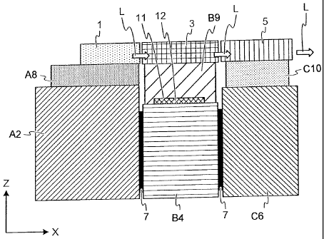
BRIEF DESCRIPTION OF DRAWINGS
[0008] FIG. 1 is a cross-sectional view of a schematic
configuration of an optical module being a laser light
source device according to a first embodiment of the
present invention;
FIG. 2 is a perspective view of a sub mount alone
composing the optical module according to the first
embodiment of the present invention;
FIG. 3 is a perspective view for illustrating a state
in which a sub mount on which a slit-like concave portion
is not provided is joined to a heat sink by means of a
CA 02710955 2013-09-04
joining material; and
FIG. 4 is a perspective view for illustrating a state
in which the sub mount according to the first embodiment of
the present invention is joined to the heat sink by means
5 of the joining material.
EXPLANATIONS OF REFERENCE CHARACTERS
[0009] 1 semiconductor laser chip
A2 heat sink A
3 solid laser
84 heat sink B
5 wavelength conversion element
C6 heat sink C
7 joining material
A8 sub mount A
B9 sub mount B
C10 sub mount C
11 concave portion
12 joining material
13 conventional sub mount
BEST MODE(S) FOR CARRYING OUT THE INVENTION
[0010] Hereinafter, embodiments of a laser light source
device according to the present invention is described in
detail with reference to the drawings. Meanwhile, the
CA 02710955 2010-06-28
6
present invention is not limited to a following description
and may be appropriately changed without departing from the
scope of the present invention.
[0011] First Embodiment
FIG. 1 is a cross-sectional view of a schematic
configuration of an optical module being the laser light
source device according to a first embodiment of the
present invention. The optical module according to the
first embodiment is an LD pumped solid laser light source
having a laser diode (LD) as a pumping source.
[0012] The optical module according to the first
embodiment is provided with a semiconductor laser chip 1, a
solid laser 3 and a wavelength conversion element 5 as
optical elements as shown in FIG. 1. The semiconductor
laser chip 1 is fixedly bonded to a heat sink A2 by means
of a joining material through a sub mount A8 as shown in
FIG. 1 for diffusing heat in the semiconductor laser chip 1.
The solid laser 3 is fixedly bonded to a heat sink B4 by
means of the joining material through a sub mount B9 as
shown in FIG. 1 for diffusing heat in the solid laser 3.
The wavelength conversion element 5 is fixedly bonded to a
heat sink C6 by means of the joining material through a sub
mount C10 as shown in FIG. 1 for diffusing heat in the
wavelength conversion element 5.
[0013] Here, each optical element is fixedly bonded to
CA 02710955 2010-06-28
7
each heat sink through the sub mount such that an end face
(side surface) of the heat sink and an end face (side
surface) of the optical element mounted on the heat sink
are substantially flush with each other. That is to say,
it is configured such that an end face (side surface) on a
solid laser 3 side of the semiconductor laser chip 1 is
substantially flush with an end face (side surface) on a
solid laser 3 side of the heat sink A2 on which the
semiconductor laser chip 1 is mounted through the sub mount
A8.
[0014] Also, it is configured such that an end face
(side surface) on a semiconductor laser chip 1 side of the
solid laser 3 is substantially flush with an end face (side
surface) on a semiconductor laser chip 1 side of the heat
sink B4 on which the solid laser 3 is mounted through the
sub mount B9. It is configured such that an end face (side
surface) on a wavelength conversion element 5 side of the
solid laser 3 is substantially flush with an end face (side
surface) on a wavelength conversion element 5 side of the
heat sink B4 on which the solid laser 3 is mounted through
the sub mount B9.
[0015] Also, it is configured such that an end face
(side surface) on a solid laser 3 side of the wavelength
conversion element 5 is substantially flush with an end
face (side surface) on a solid laser 3 side of the heat
CA 02710955 2010-06-28
8
sink C6 on which the wavelength conversion element 5 is
mounted through the sub mount C10.
[0016] Also, the heat sink A2 is joined to the heat sink
B4 by means of a joining material 7, and the heat sink B4
is joined to the heat sink C6 by means of the joining
material. The optical elements (the semiconductor laser
chip 1 and the solid laser 3, the solid laser 3 and the
wavelength conversion element 5) are optically directly
coupled with each other by means of butt joint, and it is
configured such that the heat sinks are joined to each
other in a state in which the end faces of the optical
elements are brought closer to each other with a distance
of several tens of micrometers for obtaining a sufficient
optical characteristic.
[0017] In this optical module, laser light enters the
solid laser 3 from the semiconductor laser chip 1,
amplified laser light enters the wavelength conversion
element 5 from the solid laser 3, and this is wavelength
converted and is emitted from the wavelength conversion
element 5. An optical axis of the laser light at that time
is represented by L (X-direction) in FIG. 1.
[0018] A width (X-direction in FIG. 1) of a joining
surface of the sub mount B9 with the heat sink B4 is made
shorter than a width of the heat sink B4. Also, a slit-
like concave portion 11 is provided on a rear surface of
CA 02710955 2010-06-28
9
the sub mount 39 (the joining surface of the sub mount B9
with the heat sink B4) as a groove portion extending in a
direction substantially horizontal to the joining surface
and substantially orthogonal to the direction of the
optical axis L of the laser light. Meanwhile, the groove
portion in the present invention is the groove portion,
which does not have openings on end faces (side surfaces)
on a heat sink A2 side and a heat sink C6 side of the sub
mount 39.
[0019] FIG. 2 is a perspective view of the sub mount 39
alone used in the optical module according to this
embodiment. The slit-like concave portion 11 is provided
in order to prevent an excess joining material from
overflowing on a joining surface of the heat sink B4 and
running down end faces (side surfaces) on a heat sink A2
side and a heat sink 06 side of the heat sink B4 when
joining the sub mount B9 to the heat sink 34 by means of
the joining material. That is to say, in the optical
module according to this embodiment, the excess joining
material out of the joining material for joining the sub
mount 39 to the heat sink B4 is accumulated in the slit-
like concave portion 11, so that the excess joining
material is prevented from overflowing on the joining
surface of the heat sink 34 and running down the end faces
(side surfaces) on the heat sink A2 side and the heat sink
CA 02710955 2010-06-28
C6 side of the heat sink B4.
[0020] FIG. 3 is a perspective view for illustrating a
state in which a conventional sub mount 13 on which the
slit-like concave portion 11 is not provided is joined to
5 the heat sink B4 by means of the joining material. In this
case, since the slit-like concave portion 11 is not
provided on the sub mount 13, an excess joining material 12
out of the joining material for joining the sub mount 13 to
the heat sink B4 overflows on the joining surface of the
10 heat sink B4 and runs down to the end faces (side surfaces)
of the heat sink B4. When joining the heat sink B4 to the
heat sink A2 and the heat sink 06 by bringing the optical
elements closer to each other, mechanical interference with
the heat sink A2 and the heat sink C6 is generated by the
excess joining material 12 running down to the end faces
(side surfaces) of the heat sink B4, so that it is not
possible to join the optical elements with a desired
optical characteristic.
[0021] On the other hand, since the slit-like concave
portion 11 is provided on the sub mount B9 in this
embodiment, the excess joining material 12 out of the
joining material flows in the direction substantially
orthogonal to the optical axis L along the slit-like
concave portion 11 in the sub mount B9 as shown in FIG. 4.
FIG. 4 is a perspective view for illustrating a state in
CA 02710955 2010-06-28
11
which the sub mount B9 is joined to the heat sink B4 by
means of the joining material according to this embodiment.
[0022] By preventing the joining material 12 from
protruding on the end faces (side surfaces) in the optical
axis L direction of the sub mount B9 in this manner, the
optical elements may be optically efficiently coupled with
each other by means of the butt joint. Also, it becomes
possible to make a width (X-direction) of the sub mount B9
the same as a width (X-direction) of the solid laser 3
without limit. According to this, heat generated by the
solid laser 3 may be efficiently transferred to the heat
sink B4 to be diffused.
[0023] A method of forming the slit-like concave portion
11 on the sub mount B9 includes mechanical fabrication and
a method of forming a wall portion of the groove portion by
means of plating and etching.
[0024] Although the slit-like concave portion 11 is
formed on the sub mount B9 in this embodiment, the slit-
like concave portion 11 is provided on at least one of
adjacent sub mounts (the sub mounts A8 and B9, the sub
mounts B9 and C10). Further, it is preferable that the
slit-like concave portion 11 is provided on both of the
adjacent sub mounts (the sub mounts A8 and B9, the sub
mounts B9 and C10).
[0025] A method of fabricating the optical module
CA 02710955 2010-06-28
12
according to this embodiment thus configured is described.
First, the semiconductor laser chip 1 is fixedly bonded to
the heat sink A2 by means of the joining material through
the sub mount A8. Also, the solid laser 3 is fixedly
bonded to the heat sink B4 by means of the joining material
through the sub mount B9, and the wavelength conversion
element 5 is fixedly bonded to the heat sink C6 by means of
the joining material through the sub mount C10.
[0026] Next, the heat sink B4 to which the solid laser 3
is joined is joined to the heat sink A2 to which the
semiconductor laser chip 1 is joined by means of the
joining material 7. Thereafter, the heat sink C6 to which
the wavelength conversion element 5 is joined is joined to
the heat sink B4 by means of the joining material 7. At
that time, the heat sinks are joined to each other in a
state in which the end faces of the optical elements are
brought closer to each other with the distance of several
tens of micrometers in order that the optical elements (the
semiconductor laser chip 1 and the solid laser 3, the solid
laser 3 and the wavelength conversion element 5) are
optically directly coupled with each other by means of the
butt joint for sufficiently obtaining the optical
characteristic.
[0027] As described above, in the optical module according
to this embodiment, the slit-like concave portion 11
CA 02710955 2010-06-28
13
extending in the direction substantially horizontal to the
joining surface and substantially orthogonal to the
direction of the optical axis L of the laser light in the
own device is provided on the joining surface of the sub
mount B9 with the heat sink B4. Therefore, the excess
joining material 12 out of the joining material for joining
the sub mount B9 to the heat sink B4 flows in the direction
substantially orthogonal to the optical axis L along the
slit-like concave portion 11 in the sub mount B9.
According to this, the excess joining material 12 does not
protrude on the end faces (side surfaces) in the optical
axis L direction of the sub mount B9, and the optical
elements may be optically efficiently coupled with each
other by means of the butt joint. Therefore, according to
the optical module according to this embodiment, the laser
light source device having a high-quality optical
characteristic in which deterioration of the optical
characteristic due to the excess joining material at the
time of assembly is prevented may be realized.
[0028] Also, it becomes possible to make the width (X-
direction) of the sub mount B9 the same as the width (X-
direction) of the solid laser 3 without limit. According
to this, the heat generated by the solid laser 3 may be
efficiently transferred to the heat sink B4 to be diffused.
Also, by controlling the direction in which the joining
CA 02710955 2010-06-28
14
material 12 flows, a small optical module may be obtained.
[0029] Second Embodiment
Although the case in which the slit-like concave
portion 11 is provided on the rear surface of the sub mount
B (the joining surface of the sub mount B9 with the heat
sink B4) as the groove portion is described in the above-
described first embodiment, when there is no problem in
optical performance, it is also possible to provide the
groove portion on the rear surface of the optical element
itself as described above and directly join the optical
element onto the heat sink without the sub mount.
According to this configuration, the number of components
of the optical module may be reduced, an assembly work may
be simplified and a cost may be reduced.
[0030] Third Embodiment
Although the case in which the slit-like concave
portion 11 is provided on the rear surface of the sub mount
B (the joining surface of the sub mount B9 with the heat
sink B4) as the groove portion is described in the above-
described first embodiment, the shape of the groove portion
may be any shape as long as this may control the flow
direction of the excess joining material =12 generated when
joining the sub mount B9 to the heat sink B4 to allow to
flow in the direction substantially orthogonal to the
optical axis L, and the groove portion such as a triangle
CA 02710955 2010-06-28
groove may be provided, for example. A method of forming
the groove portion such as the triangle groove on the sub
mount B9 includes the mechanical fabrication and the method
of forming the wall portion of the groove portion by means
5 of plating and etching.
[0031] Fourth Embodiment
Although the case in which the slit-like concave
portion 11 is provided on the rear surface of the sub mount
B (the joining surface of the sub mount 59 with the heat
10 sink 54) is described in the above-described first
embodiment, the slit-like concave portion may be formed in
the direction substantially orthogonal to the optical axis
L as the groove portion on the joining surface of the heat
sink B4 with the sub mount B9. In this case also, the same
15 effect as in the case in which the slit-like concave
portion 11 is provided on the rear surface of the sub mount
B (the joining surface of the sub mount B9 with the heat
sink B4) as the groove portion may be obtained.
[0032] In this case also, the shape of the groove
portion may be any shape as long as this may control the
flow direction of the excess joining material 12 generated
when joining the sub mount B9 to the heat sink B4 to allow
to flow in the direction substantially orthogonal to the
optical axis L, and the groove portion such as the triangle
groove may be provided, for example.
CA 02710955 2010-06-28
16
[0033] The method of forming the groove portion such as
the triangle groove on the sub mount B9 and the heat sink
B4 includes the mechanical fabrication and the method of
forming the wall portion of the groove portion by means of
plating and etching.
INDUSTRIAL APPLICABILITY
[0034] As described above, the laser light source device
according to the present invention is useful as the laser
light source device in which a plurality of optical
elements are optically directly coupled with each other by
means of the butt joint.