Note: Descriptions are shown in the official language in which they were submitted.
CA 02711033 2010-06-29
WO 2010/042184 PCT/US2009/005503
1
METHOD OF SHIPPING AND TRACKING INVENTORY
CROSS-REFERENCE TO RELATED APPLICATIONS
This application claims the benefit of U.S. Application Serial No.
12/574483, filed October 6, 2009, entitled "METHOD OF SHIPPING AND
TRACKING INVENTORY"; U.S. Provisional Application No. 61 / 103472, filed
on October 7, 2008, entitled "UNIVERSAL TRACKING SYSTEM", and contains
material related to U.S. Application Serial No. 12/401,441, filed on March 10,
2009 entitled "UNIVERSAL TRACKING ASSEMBLY"; and U.S. Application
Serial No. 12/566337, filed on September 24, 2009 entitled "METHOD OF
SHIPPING AND TRACKING INVENTORY", all of which are hereby
incorporated by reference in their entireties.
FIELD OF INVENTION
The present invention relates, in general, to a method of shipping and
tracking inventory, and deals more particularly with a method of shipping and
tracking inventory in which one or more circuits of a hybrid EAS tag are
activated or deactivated based on relevant shipping criteria.
BACKGROUND OF THE INVENTION
Bar codes are commonly utilized throughout the commercial and retail
worlds in order to accurately determine the nature, cost and other vital data
of
an individual item. Bar codes, however, are purely passive constructs, and
therefore cannot offer or transmit information themselves, instead relying
upon
known bar code readers to scan and interpret the information stored in the bar
code itself. Moreover, the information content of bar codes is static, and
cannot
be changed or supplemented at will once the bar code is fabricated.
In recent years, differing electronic article surveillance (EAS)
platforms/ tags have been developed to address the shortcomings of known bar
code systems. One such type of EAS is radio frequency identification (RFID)
platforms/ tags. RFIDs are small (typically) battery-less microchips that can
be
CA 02711033 2010-06-29
WO 2010/042184 PCT/US2009/005503
2
attached to consumer goods, cattle, vehicles and other objects to track their
movement. RFID tags are normally passive, but are capable of transmitting data
if prompted by a reader. The reader transmits electromagnetic waves that
activate the RFID tag. The tag then transmits information via a predetermined
radio frequency, or the like. This information is then captured and
transmitted
to a central database for suitable processing.
An RFID system typically is made up of a transponder, or tag, which is an
integrated circuit (IC) connected to an antenna, which is then generally
embedded into labels, a reader which emits an electromagnetic field from a
connected antenna, and an enterprise system. The tag draws power from the
reader's electromagnetic field to power the IC, and broadcasts a modulated
signal which the reader picks up (via the antenna), decodes, and converts into
digital information that the enterprise system uses.
There are two main types of RFID devices, including an inductively
coupled RFID tags (otherwise known as high frequency (HF) tags). Typically,
there are three main parts to an inductively coupled RFID tag:
= Silicon microprocessor - These chips vary in size depending on their
purpose;
= Metal coil - Made of copper or aluminum wire that is wound into a
circular pattern on the transponder, this coil acts as the tag's antenna. The
tag transmits signals to the reader, with read distance determined by the
size of the coil antenna. These coil antennas can operate at 13.56 MHz;
and
= Encapsulating material - glass or polymer material that wraps around
the chip and coil.
Inductive RFID tags are powered by the magnetic field generated by the
reader. The tag's antenna picks up the magnetic energy, and the tag
communicates with the reader. The tag then modulates the magnetic field in
order to retrieve and transmit data back to the reader. Data is transmitted
back
to the reader, which directs it to the host computer and/or system.
Inductive RFID tags are very expensive on a per-unit basis, costing
anywhere from $1 for passive button tags to $200 for battery-powered, read-
CA 02711033 2010-06-29
WO 2010/042184 PCT/US2009/005503
3
write tags. The high cost for these tags is due to the silicon, the coil
antenna and
the process that is needed to wind the coil around the surface of the tag.
Another type of known RFID are capacitively coupled RFID tags. These
tags do away with the metal coil and use a small amount of silicon to perform
that same function as a inductively coupled tag. A capacitively coupled RFID
tag also has three major parts:
= Silicon microprocessor - Motorola's BiStatix RFID tags use a silicon chip
that is only 3 mm'. These tags can store 96 bits of information, which
would allow for trillions of unique numbers that can be assigned to
products;
= Conductive carbon ink - This special ink acts as the tag's antenna. It is
applied to the paper substrate through conventional printing means; and
= Paper - The silicon chip is attached to printed carbon-ink electrodes on
the back of a paper label, creating a low-cost, disposable tag that can be
integrated on conventional product labels.
By using conductive ink instead of metal coils, the price of capacitively
coupled tags are as low as 50 cents. These tags are also more flexible than
the
inductively coupled tag. Capacitively coupled tags can be bent, torn or
crumpled, and can still relay data to the tag reader. In contrast to the
magnetic
energy that powers the inductively coupled tag, capacitively coupled tags are
powered by electric fields generated by the reader. The disadvantage to this
kind of tag is that it has a very limited range.
As the two preceding examples of known RFID devices indicates, there
does not presently exist an industry-standard RFID protocol. With different
manufacturers utilizing different RFID devices on their disparate products,
large
department stores, warehouses and/or shipping containers often contain a
plurality of differing RFID devices.
It will therefore be readily appreciated that a large retail seller or shipper
having many different products, each with different RFID devices attached
thereto, may have great difficulty in matching the proper reader and
associated
protocol with the appropriate RFID tag, during an attempted interrogation of
the RFID tag.
CA 02711033 2010-06-29
WO 2010/042184 PCT/US2009/005503
4
It is therefore necessary for retail establishments and shippers to purchase
and employ multiple RFID readers and protocols, in order to ensure that every
item in their inventory has been properly interrogated and categorized, as
appropriate, and in accordance with the particular type of RFID device
attached
thereto. This undesirable duplication of readers and related machinery, and
protocols, is obviously complex and costly.
Still further, known RFID devices are designed so that they may continue
to communicate with extraneous readers well after the time of initial
purchase.
That is, known RFID devices are designed so that tracking of an item can be
accomplished from the time the item leaves the factory, until it rest within
the
residential dwelling of its purchaser.
The very attributes, however, of known RFID devices that permit these
devices to continue to operate and communicate with a reader well after the
time of initial purchase, also poses problems for closely nested commercial or
retail facilities.
For example, once a purchaser buys an item at a store, the RFID device
will communicate with an integrated reader at the checkout. The reader will
detect and interrogate the RFID device, and thereafter permit the purchaser to
exit the store without setting of an alarm for shoplifting. But because of the
resilient nature of the RFID devices, these devices continue to be passively
'active' even if the purchaser goes into another retail establishment, as
often
happens in a mall or shopping center environment. Once the original purchaser
leaves the second retail store, the RFID detection equipment in the second
store
may awaken the RFID tag, and erroneously alert the security system of the
second store. This scenario is only worsened by the differing RFID devices and
protocols that currently exist in the market.
In addition to the differing RFID technologies mentioned above, other
EAS technologies exist having their own operational protocols, such as acousto-
magnetic (AM) EAS circuitry. Similar to the problems noted above, the problem
for, e.g., manufacturer is the uncertainty of knowing which EAS technology
will
be employed at various stages of the manufacture, transportation and inventory
of items equipped with one of the many differing EAS technologies.
CA 02711033 2010-06-29
WO 2010/042184 PCT/US2009/005503
It will therefore be appreciated that the primary EAS protocols in place
are the acousto-magnetic (AM) type and the RF type, as discussed above. These
differing EAS protocols are each independently used by various major retailers
and are currently not compatible technologies. Thus, a manufacturer/
5 distributor must maintain separate inventories of their products for the
different
EAS protocols incurring the added cost in doing such a practice or the
manufacturer/distributor must apply both tags/labels to each of their products
incurring the added cost of this alternative practice.
With the forgoing problems and concerns in mind, it is the general object
of the present invention to provide a universal tracking system that is
capable of
harmonizing the use of differing EAS technologies/ devices by integrating more
than one such technology on a common susbstrate/patform. More preferably, it
is the general object of the present invention to provide an integrated EAS
label/ tag assembly, which is compatible with both AM type and RF (including
RFID) systems. The invention more preferably includes the AM type
transponder which is composed of one or more amorphous alloy strips with a
high magnetic permeability and a magnetic biasing strip which can be cast, die
cut, painted, printed, etc. The amorphous strip(s) are packaged such that they
can freely resonate and is (are) sized to resonate at the desired frequency of
standard AM type EAS.
SUMMARY OF THE INVENTION
It is one object of the present invention is to provide a universal tracking
assembly.
It is another object of the present invention is to provide a universal
tracking assembly that is capable responding to more than one EAS
interrogation protocols.
It is another object of the present invention is to provide a universal
tracking assembly that integrates differing EAS identification technologies
upon
a common platform.
CA 02711033 2010-06-29
WO 2010/042184 PCT/US2009/005503
6
It is another object of the present invention is to provide a universal
tracking system that integrates both RF and AM EAS identification technologies
upon a common platform.
It is yet another object of the present invention to provide a combined
electronic article surveillance (EAS) tag/label assembly which is capable of
being detected by, and of responding to, interrogation by either AM or RF
technologies / protocols.
It is yet another object of the present invention to provide a combined
electronic article surveillance (EAS) tag/label which is capable of utilizing
at
least one common element in support of the combined AM and RF
technologies / protocols.
It is yet another important aspect of the present invention to provide a
combined EAS tag/ label wherein the biasing magnet of the AM circuitry is
integrated into both the AM and RF circuitry, thereby affecting the
capacitance
of the combined EAS tag/label.
It is yet another important aspect of the present invention to provide a
combined EAS tag/ label wherein the biasing magnet of the AM circuitry is
positioned adjacent the inductive coil of the RF circuitry, thereby affecting
the
capacitance of the combined EAS tag/label.
Thus, it is an object of the present invention is to make a hybrid (i.e.,
combined) and selectively deactivatable EAS tag/ label that can be detected by
both AM EAS detectors and RF EAS detectors (also including RFID). The
manufacture/design of this hybrid EAS tag/label is such that the intrinsic
properties of the components enhance the performance of the overall hybrid
label / tag and that the manufacturing efficiencies allow for a less expensive
EAS
solution for the manufacturer/distributor.
These and other objectives of the present invention, and their preferred
embodiments, shall become clear by consideration of the specification, claims
and drawings taken as a whole.
BRIEF DESCRIPTION OF THE DRAWINGS
Figure 1 schematically illustrates a known RFID EAS assembly.
CA 02711033 2010-06-29
WO 2010/042184 PCT/US2009/005503
7
Figure 2 schematically illustrates another known RFID EAS assembly.
Figure 3 schematically illustrates another known RFID EAS assembly.
Figure 4 schematically illustrates another known RFID EAS assembly.
Figure 5 schematically illustrates an integrated RFID EAS assembly
according to one embodiment of the present invention.
Figure 6 schematically illustrates an integrated RFID EAS assembly
according to another embodiment of the present invention.
Figure 7 illustrates a flow diagram pertaining to the integrated RFID EAS
assembly of Figure 6.
Figure 8 illustrates a top plan view of a combined EAS tag/ label assembly
exhibiting integrated AM and RF components, according to a preferred
embodiment of the present invention.
Figure 9 illustrates a side view of the combined EAS tag/label assembly
shown in Figure S.
Figure 10 illustrates a flow diagram showing the selective activation/
deactivation of either the AM or RF portions of the combined EAS tag/label
assembly shown in Figures 8-9.
Figure 11 illustrates a schematic view of a universal tracking assembly in
accordance with an alternative embodiment of the present invention.
Figure 12 illustrates a side view of the universal tracking assembly of
Figure 11.
Figure 13 illustrates a graph depicting a Q value associated with the
universal tracking assembly of Figure 11.
Figure 14 is a flow diagram depicting a method of shipping and tracking
inventory in accordance with an embodiment of the present invention.
Figure 15 graphically illustrates a system by which the method of Figure
14 may be utilized.
Figure 16 is a flow diagram depicting a method of shipping and tracking
inventory in accordance with another embodiment of the present invention.
Figure 17 is a flow diagram depicting a method of shipping a tracking
inventory in accordance with an additional embodiment of the present
invention.
CA 02711033 2010-06-29
WO 2010/042184 PCT/US2009/005503
8
DETAILED DESCRIPTION OF THE PREFERRED EMBODIMENTS
Known EAS assemblies, such as RFID tags, can be either active or passive.
Active RFID tags include a battery, or the like, and so are capable of
transmitting
strong response signals even in regions where the interrogating radio
frequency
field is weak. Thus, an active RFID tag can be detected and transmit at a
greater
range than is possible with a passive RFID. Batteries, however, are limited in
their operable lifetime, and add significantly to the size and cost of the
tag. A
passive tag derives the energy needed to power the tag from the interrogating
radio frequency field, and uses that energy to transmit response codes by
modulating the impedance the antenna presents to the interrogating field,
thereby modulating the signal reflected back to the reader antenna. Thus,
their
range is more limited.
Even within known passive RFID tags, there exists significant differences
in performance, including significant differences in the performance of their
associated antennas and corresponding interrogation and response ranges.
While one embodiment of the present invention will be hereafter described in
connection with passive tags, it will be readily appreciated that the
teachings of
the present invention are equally applicable to active tags.
Figure 1 illustrates one version of a passive RFID 10, which typically
includes an integrated circuit 12 and an antenna 14. The integrated circuit 12
provides the primary identification function. It includes software and
circuitry
to permanently (or semipermanently) store the tag identification and other
desirable information, interpret and process commands received from the
interrogation hardware, respond to requests for information by the
interrogator,
and assist the hardware in resolving conflicts resulting from multiple tags
responding to interrogation simultaneously. Optionally, the integrated circuit
may provide for updating the information stored in its memory (read/ write) as
opposed to just reading the information out (read only).
The antenna geometry and properties depend on the desired operating
frequency of the RFID portion of the tag. For example, 2.45 GHz (or similar)
RFID tags would typically include a dipole antenna, such as the linear dipole
CA 02711033 2010-06-29
WO 2010/042184 PCT/US2009/005503
9
antennas 4a shown in Figure 1, or the folded dipole antennas 14a shown
attached to the passive RFID 10a in Figure 2. A 13.56 MHz (or similar) RFID
tag
would use a spiral or coil antenna 14b, as shown in the RFID 10b of Figure 3.
Regardless of the particular design, the antenna 14 intercepts the radio
frequency energy radiated by an interrogation source. This signal energy
carries
both power and commands to the tag. The antenna enables the RF-responsive
element to absorb energy sufficient to power the IC chip and thereby provide
the response to be detected. Thus, the characteristics of the antenna must be
matched to the system in which it is incorporated. In the case of tags
operating
in the high MHz to GHz range, the most important characteristic is the antenna
length. Typically, the effective length of a dipole antenna is selected so
that it is
close to a half wavelength or multiple half wavelength of the interrogation
signal. In the case of tags operating in the low to mid MHz region (13.56 MHz,
for example) where a half wavelength antenna is impractical due to size
limitations, the important characteristics are antenna inductance and the
number
of turns on the antenna coil. For both antenna types, good electrical
conductivity is required. Typically, metals such as copper or aluminum would
be used, but other conductors, including magnetic metals such as permalloy,
are
also acceptable.
Figure 4 illustrates a passive RFID tag 10c which utilizes a conductive ink
portion 14c to act as the antenna for the RFID 10c. Although less expensive to
fabricate than RFID tags that include a wound wire antenna array, the
conductive ink antenna 14c is limited in range and power.
In sum, therefore, there exists several differing types of RFID tags, which
can either incorporate a magnetically responsive element, or a RF responsive
element. As will be understood, each of these differing types of tags require
differing interrogation devices and protocols so as to effectively interact
with
each tag type. This situation is difficult for large retailers, or the like,
who
inevitably accept product from a vast array of manufacturers utilizing
differing
RFID tag types.
Figure 5 illustrates, therefore, one embodiment of the present invention.
As shown in Figure 5, a single, integrated RFID tag 20 includes both a
magnetically-responsive RFID 22 and an RF-responsive RFID 24. When so
CA 02711033 2010-06-29
WO 2010/042184 PCT/US2009/005503
coupled on a single RFID tag, these two RFID tag-types ensure that whatever
type of interrogation device is employed by a user or, e.g., a retail store,
the
system will be able to communicate with at least one of the tags 22/24.
It is therefore an important aspect of the present invention that more than
5 one type of RFID tag be integrated into a single RFID tag. By doing so the
present invention ensures that regardless of the interrogation system utilized
at
or in any particular location, at least one of the integrated RFID tags will
respond to the interrogation with the required information. Thus, a retail
store
need only buy a single interrogation system, without fear of not being able to
10 communicate with those items having RFID tags of differing types.
It will be readily appreciated that the present invention is not limited to
the integration of magnetically-responsive RFIDs and RF-responsive RFIDs
together, and extends to the integration of RFID tags of any known, or to be
discovered, type.
It is a further object of the present invention that significant elements
present in one RFID tag may be universally utilized with respect to the other
integrated RFID tags present on the integrated RFID tag 20. For example,
should the integrated RFID tag 20 support both the RFID tags of Figures 3 and
4,
the RFID tag of Figure 4 could utilize the antenna 14b of the RFID tag in
Figure
3, thereby increasing the range of the conducive-ink RFID tag illustrated in
Figure 4.
It will be readily appreciated that the common use of a single component
between differing RFID tags is not limited to the sharing of an antenna
element.
Indeed, the present invention equally contemplates the shared use of any
component found in any RFID tag that are jointly mounted on a unitary
platform.
Figure 5 illustrates the shared use of a battery, or power supplying
element, 26 with both of the RFIDs 22 / 24. The use of a shared or common
power source 26 effectively removes the range limitations associated with
certain types of RFID tags, as well as being more economically practical than
providing a separate power source for each of the integrated RFIDs.
As discussed previously, large retailers, or the like, often accept
merchandise from a variety of manufacturers who may be located at disparate
CA 02711033 2010-06-29
WO 2010/042184 PCT/US2009/005503
11
points around the world. Each of these individual manufacturers may place an
RFID tag of their choosing on the item as it is produced. This item is then
transported by a shipper who may also place another RFID tag on the item, in
accordance with the particular RFID system/ configuration the shipper
utilizes.
Finally, the retailer itself may place yet another RFID tag on the item, again
of its
own choosing and configuration, and one which operates well with the
interrogation system employed by the retailer.
In sum, any given item may have a plurality of differing RFID tags
located, glued or otherwise attached thereto. Thus, while the retailer may
deactivate their RFID tag placed on the item as the customer leaves the store,
a
problem exists when the retailer's deactivation system does not communicate
with the other types of RFID tags that may also be located in or on the item.
When one or more of the additional RFID tags on a given item are not
suitably deactivated, owing to their differing configurations and protocols,
it is
possible that the consumer may walk into another, non-affiliated store with
the
first item purchased, only to have the non-deactivated RFIDs set off the
security
system of the second store.
The integrated nature of the RFID tag 20 shown in Figure 5 removes the
possibility of any such erroneous indications of shoplifting, or the like,
caused
by the non-deactivated RFID tags. Figure 6 illustrates an integrated RFID tag
30,
supporting an array of six differing RFID tags 32. It will be readily
appreciated
that there be more or less RFID tags 32 formed on the integrated RFID tag 30,
without departing from the broader aspects of the present invention.
Figure 7 is a flow diagram illustrating the operation of the integrated
RFID tag 30 shown in Figure 6. As depicted in step 34, an interrogator (such
as
one of the known RFID readers) is utilized to scan or interrogate the RFID tag
32. The interrogator then identifies one or more RFID tags 32 present in the
array which are compatible with the technology of the interrogator, in step
36.
The interrogator will then issue a command or signal to deactivate those RFID
tags in the array which are compatible with the interrogator, as depicted in
step
38. Following this, in step 40, the deactivation signal is communicated
internally
of the RFID tag 30, to the non-deactivated RF1D tags 32, thereby deactivating
all
of the RFID tags 32, regardless of their configuration or protocol.
CA 02711033 2010-06-29
WO 2010/042184 PCT/US2009/005503
12
It is therefore another important aspect of the present invention that the
integrated nature of the RF1D tag 30 enables the complete deactivation of all
of
the RFID tags 32 anytime when the interrogator is capable of deactivating even
one of the RFID tags 32 in the array. Thus, once a consumer purchases an item,
and the interrogation system employed by the retail store deactivates the
store
RFID, the present invention ensures that all other RFIDs (or other types of
EAS
assemblies, as discussed in more detail later) in the array will also be
deactivated. Erroneous indication of shoplifting or the like, as the consumer
moves from store to store with a previously purchased item, are thereby
avoided.
The communication between the RFID tags 32 may be accomplished
through a direct electrical connection, or filament, 44 (as shown in Figure
6), or
via electromagnetic coupling, such as parasitic coupling, capacitive coupling
or
inductive coupling.
When employing the combined (or, integrated) RFID tag 30 in accordance
with the present invention, none of the existing industries or retail stores
need
change the protocol by which they interrogate their combined RFID tags,
regardless of the technology underpinning each of the differing RFID circuitry
supported thereon. That is, regardless of the interrogation or reader
apparatuses
utilized by the various manufacturing and retail outlets, an integrated and
combined EAS tag assembly will always have at least one type of RF circuitry
that is capable of communicating with the respective interrogator or reader.
Given the differing technologies currently utilized by various
manufacturers of RFID EAS tags, and the anticipated continuing evolution of
technology in this area, the integrated RFID tag of the present invention
effectively mimics a universal standard of RFID technology and related
interrogators/readers, which does not currently exist. Thus, until such a
standard is accepted worldwide, the integrated RFID tag of the present
invention provides a platform upon which to mask the differences between the
competing RFID technologies.
Other embodiments of the present invention can be visualized by a
review of the foregoing. As to the integrated RFID tag 20 shown in Figure 5,
the
CA 02711033 2010-06-29
WO 2010/042184 PCT/US2009/005503
13
present invention equally contemplates that the deactivation signal
communicated to either the RFID 22 or 24 is likewise communicated to the
common power source 26. By changing the state of the power source, the
deactivation of the RFID 22 will effectively also deactivate the RFID 24.
Figures 5-7 therefore exhibit related embodiments of a combined EAS
assembly having a plurality of RFID technologies integrated thereon. Thus, the
combined EAS assemblies shown in Figures 5-7 are capable of responding to
interrogation by differing RFID protocols.
In yet another, preferred, embodiment of the present invention, a
combined EAS assembly 50 is shown in Figures 8-9. As shown in Figures 8-9,
the combined EAS assembly 50 integrates both AM and RF components and
technologies in a single, combined and universal EAS tag/label assembly.
The combined EAS tag assembly 50 includes a first portion 52 of a RF
component which exhibits inductance, a second portion 54 of a RF component
which exhibits capacitance, a third multi-layer portion 56 of an AM component
including a resonator and a bias magnet, and a fourth portion 58 acting as the
substrate and backing of the combined EAS tag 50. As shown in Figure 9, the
third multi-layer portion 56 includes an amorphous resonator 60 and a bias
magnet 62.
Known RF resonators are typically configured as a LC Tank circuit,
typically consisting of simply an inductor and capacitor(s). In contrast, the
EAS
tag assembly 50 will capture the resonant frequency of both the RF and AM
components of the label and allow for a space in the center of the RF circuit
to
place the AM type label. The AM portion can be placed at various locations on
the RF circuit, but interactions have to be accounted for and the RF portion
must
be tuned. Placing the AM components in the center of an open space in a RF
circuit will primarily effect the inductance. Placing the AM portion in other
locations could effect inductance, depending on the means of attaching or the
dielectric, and certainly capacitance. Either way, once the AM portion is
positioned in an inactive state, the RF portion is designed around the AM
components and tuned to accommodate the interaction for any capacitance or
inductance effects. This tuning will account for center frequency and the
quality
of the circuit.
CA 02711033 2010-06-29
WO 2010/042184 PCT/US2009/005503
14
The RF label components can be produced by various manufacturing
methods such as die cutting, laser cutting, hot foil printing, embossing,
printing
with conductive inks, etc... The method of manufacture is secondary in
importance to the design of the RF portion of the combined EAS tag assembly
50. The means and location of the AM circuitry portion in relation to the RF
circuitry portion will affect the advantage of shielding properties. The RF
label
component in accordance with the embodiment shown in Figures 8-9 can
therefore be generally formed or stamped out of a material and forming the LC
tank circuit which resonates at the desired frequency. The LC tank circuitry
may
itself be formed by layering "foils" (or inks, etc.) with designed dielectrics
to
form the inductor and plate capacitors.
It is therefore another important aspect of the present invention that the
RF subsystem of the EAS tag assembly/ label 50 is formed in a way and with
specific materials that the combined EAS tag/ label assembly 50 resonates at
the
appropriate frequency as an AM label would.
Similar to known AM labels, the subsystem of the EAS tag assembly 50
will continue to include the bias magnet 62, one or more resonators 60 cut
from
an amorphous alloy such as MetGlas (Metglas 2826MB3 has been used, however
it will be readily appreciated that the present invention is not limited by
this
particular alloy), and packaging to allow for magnetorestriction and
resonance.
It is therefore another important aspect of the present invention that the
design of the EAS tag assembly 50 allows for at least one of these AM circuit
components to be part of the RF circuit. The balance/ tuning of the AM
subsystem is effected at least in part by the inclusion of additional
resonators
and shaping of the primary to not only accomplish the RF subsystem, but
contribute to the resonance of the AM subsystem. These AM label components
may also be produced by a variety of manufacturing methods and may include
die cutting, printing the bias magnet, etc. It will be readily appreciated
that the
specific method of manufacture either the RF or AM components of the EAS tag
assembly 50 is secondary to the design of the combined EAS tag assembly 50,
and that the present invention is not limited by the manner in which the EAS
tag
assembly is manufactured.
CA 02711033 2010-06-29
WO 2010/042184 PCT/US2009/005503
Yet, another important aspect of the present invention is that the design
of the EAS tag assembly 50 will allow for only one portion to be active at a
given
time. Thus, when the tag is activated for AM, it is deactivated for RF. This
is
5 coincident with the intrinsic properties of the labels themselves, as
expressed:
AM RF
Activation Magnetize De-magnetize
De-Activation De-magnetize Magnetize RF
Shorting
Thus, in a preferred embodiment, the resonator component (which may
be formed from Metglas or from many of the known amorphous alloys, used for
10 the magnetorestrictive resonator) will be employed as not only the
resonator in
the AM subsystem, but may be a layer or a portion of a layer of the RF
subsystem. The bias magnet 62 may also be a layer or a portion of a layer.
Moreover, the resonator component can also be effective for EMF
shielding. As such, when a shield is placed behind the RF component, the
signal
15 from the RF is not absorbed by the package that it is trying to protect,
but is
directed outward toward the EAS gate which is meant to detect the signal. The
shielding aspect can coexist with the actual performance of both the AM and
the
RF components when the RF circuit is designed and tuned to accommodate the
interaction between the two. However, as stated previously, the means and
location of the AM portion in relation to the RF portion will effect the
advantage
of shielding properties.
It will therefore be readily appreciated that with the combined EAS tag
assembly 50, a manufacturer can incorporate the label / tag 50 into a product
or
packaging during manufacture and maintain a single inventory. When the
order for a product comes in, the products are picked and then the appropriate
AM or RF component is activated/ deactivated. This can be done automatically
on a conveyor system or individually. A flow chart depicting the simplicity of
this is shown in Figure 10.
Thus, a preferred embodiment of the present invention provides an
integrated EAS label/ tag assembly 50 which is compatible with both AM type
CA 02711033 2010-06-29
WO 2010/042184 PCT/US2009/005503
16
and RF (including RFID) systems. The invention includes the AM type
transponder which is composed of one or more amorphous alloys strips with a
high magnetic permeability and a magnetic biasing strip which can be cast, die
cut, painted, printed, etc... The amorphous strip(s) are packaged such that
they
can freely resonate and is (are) sized to resonate at the desired frequency of
standard AM type EAS.
The invention also includes the RF (or RFID) component which can be
manufactured by any number of know processes. The process of die cutting or
laser cutting the material is the preferred method (however, any number of
methods may be used), since it minimizes the steps of manufacture, amount of
equipment and eases the capability of mass producing a fine tuned RF type EAS
tag exhibiting the rectangular shape with open space in its center and/or for
fine
tuning the interaction between the components regardless of their location and
RF antenna type. An open space is preferred when combining the two types of
tag/ labels (AM and RF) to maximize shielding effects. However, the open space
is not necessarily to create a highly functional combined/ universal tag,
which
provides the business benefit of reducing inventory and the associated costs.
Moreover, The RF subsystem of the combined EAS tag / label assembly 50
is characterized as a LC Tank Circuit where the angular frequency is equal to:
1
w = Pang = LC in radians/ sec ; where L is in Henries and C is in Farads;
Resonant Frequency is equal to:
Measured w = Ffes in radians sec where L is in Henries and C is in Farads;
r-Lz-c-
in Hertz
CO F= _
2*jr 2*n* LC
The AM subsystem of the combined EAS tag/ label assembly 50 is
characterized by one or more strips or ribbons of an amorphous
magnetorestrictive alloy, which is magnetically biased by the placement of the
bias magnet. The resonator(s) provide consistent resonant frequency when a
given bias field is applied. Although it is common to have multiple
resonators,
CA 02711033 2010-06-29
WO 2010/042184 PCT/US2009/005503
17
the design of the present invention does not preclude the use of a single
resonator or multiple arrangement. In simplistic terms, resonators of the same
thickness can be accomplished as long as the length is constant and total
width
is approximately the same. For approximation, if a single resonator can be
designed with a length of approximately 38mm and a width of 2x, two
individual resonators of the same length can be used with a width of x,
assuming consistent thickness.
The combined RF (including RFID) and AM label / tag provides the
overall system with not only a less expensive means of manufacturing these
labels/ tags independently, but provides a potential improvement in
performance and product shielding. Depending upon the position of the AM
portion in relation to the RF portion, shielding may be improved. The
resonators, being an amorphous alloy, are intrinsic shielding materials.
Customized designs following this method allow that the RF signature will not
be absorbed by the product being labeled, since the amorphous alloys used as
resonators in the AM tag will shield the product and reflect the signal
outward
in the desired direction.
It is therefore an important aspect of the present invention that the
combined EAS tags described in connection with the embodiments of Figures
5-10 each contain at least a first and a second circuit portions, each of
which are
capable of excitation (or 'interrogation', by a suitable reader/writer) by
separate
technological protocols. Thus, a combined EAS tag/ label assembly is created
which may properly communicate with any number of differing interrogation
protocols, regardless of the technology protocol of the interrogator/reader.
It will also be appreciated that the disclosed embodiments as presented in
connection with Figures 5-10 are not limiting in the nature of the EAS
circuitry
integrated in the combined EAS tag/label. That is, any number or differing
types of EAS circuitry, in existence now or developed in the future, may be
integrated onto a common substrate of an EAS tag /label, without departing
from the broader aspects of the present invention. Moreover, although the
present invention envisions integrating differing types of EAS circuitry onto
a
common substrate, each being capable of excitation/ interrogation by the
appropriate interrogation protocols, the combined EAS tag/ label of the
present
CA 02711033 2010-06-29
WO 2010/042184 PCT/US2009/005503
18
invention seeks to utilize at least one common element, or component, between
the differing EAS circuitry. In this manner, a reduction in the overall size
and
cost of the combined EAS tag/ label assembly of the present invention is
realized.
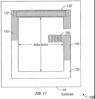
Referring now to Figures 11-13, an alternative embodiment of the
inventive tracking assembly is disclosed. More specifically, the depicted
embodiment is an EAS tracking tag/label that includes both an RF circuit and
an
AM circuit in a single, stacked hybrid assembly. The stacked configuration of
the hybrid RF/AM assembly is facilitated through the use of a bias magnet as a
shared component between the RF and AM circuits.
As shown in Figures 11 and 12, the inventive tag 100 includes a substrate
110. As will be appreciated, the substrate 110 may be manufactured from a
variety of materials including paper and the like. The substrate 110 has an
adhesive layer 120 (Figure 12), which secures the hybrid RF/AM circuit to the
substrate 110. The substrate 110 may also have an attachment surface or
backing
115 with a peel-off layer allowing the substrate 110 to be secured to a
package.
Affixed to the substrate 110 is a coil inductor 130 of the RF circuit, which
as discussed above, is an LF tank circuit. As shown, a portion of the coil
inductor 130 is overlapped by another section of foil or magnetic ink, thereby
forming a plate capacitor 140. As mentioned, the capacitor 140 is preferably a
second layer of foil that has been secured to the inductor 130 with dielectric
glue.
The capacitor 140 also has a plurality of cut-away portions 180 which can be
broken or blown out with high-energy RF to disable the RF portion of the
inventive tag should the tag be for use with AM readers exclusively.
The coil inductor 130 may itself be manufactured from a foil or a metallic
ink. Preferably, the coil inductor 130 is foil and is manufactured using a die
cut
process in which the inductor 130 and capacitor 140 are cut from a single
piece
of foil. When cut from a single piece of foil, the die cut foil would include
a fold
line allowing the 'capacitor' portion 140 to be folded over the 'inductor'
portion
130, and glued in place. The size of the inductor 130 may vary provided that
it
has a width large enough to accommodate the bias magnet and the resonator
strips of the AM circuit, as will be discussed in more detail below.
CA 02711033 2010-06-29
WO 2010/042184 PCT/US2009/005503
19
Referring again to Figures 11 and 12, the coil inductor 130 has a layer of
dielectric material 145 separating it from a bias magnet 150. The bias magnet
150
is preferably a unitary single piece magnet and, as is known, is typically
employed in AM-type EAS tags. While a single-piece magnet has been
described, the present invention is not so limited in this regard, as the
magnet
may alternatively be formed as a multi-piece structure, without departing from
the broader aspects of the present invention. Indeed, a primary concern is
that
the magnetic component evidence two spaced apart poles, regardless of the
specific structure of the bias magnet 150. Moreover, and with respect to
employing spaced apart poles, the poles being located on a portion of the
inductor and capacitor, a substantial cost savings may be realized over the
use of
a single piece bias magnet, as less magnetic material would obviously be
required.
In its preferred configuration, however, the bias magnet 150 is a single
unitary 38 mm x 4 mm Arnochrome permanent magnet that is situated so that it
overlaps, in superposition, both a portion of the inductor 130 and plate
capacitor
140 on top of the inductor 130. Importantly, in this location, the bias magnet
150
increases the capacitance of the RF circuit and becomes, in essence, part of
the
capacitor 140. Indeed, the area of overlap between the plate capacitor 140 and
inductor 130 can be reduced or expanded in accordance with the size of the
bias
magnet 150 to achieve a desired resonance frequency.
As will be appreciated, the bias magnet 150 is a preferred shared
component between the RF circuit and the AM circuit in the inventive hybrid
assembly of the present embodiment. The AM portion of the assembly includes
the bias magnet 150 and multiple resonator strips 170 located within an
insulative bubble-type enclosure or pack 160, preferably manufactured from
plastic. The resonator strips 170 may be formed from Metglas or from many
known amorphous alloys. The bubble pack 160 is insulative so that the
resonator strips do not affect the capacitance of the RF circuit. Preferably,
the
bubble pack 160 is secured to the bias magnet 150 by gluing the edges of the
pack 160 directly to the bias magnet 150.
The use of the bias magnet 150 in the RF circuit is an important aspect of
the present invention. The bias magnet 150 effectively increases the
capacitance
CA 02711033 2010-06-29
WO 2010/042184 PCT/US2009/005503
of the RF circuit, while also allowing the AM portion to be stacked directly
on
top of the RF portion without destroying the functioning of either the AM or
RF
portions of the universal tracking tag/assembly 100.
Indeed, simply mounting an AM circuit and RF circuit, in close
5 association on the same tag substrate, serves to interfere with the
capacitance of
the RF circuit, e.g., thereby reducing the resonance frequency from the (e.g.)
required 8.2 MHz, and potentially rendering both circuits unsuitable for use.
In sharp contrast, the present invention has determined that by
employing the bias magnet 150 (a necessary component of known AM circuitry)
10 in a superpositional orientation over the existing coil inductor of the RF
circuitry, the bias magnet 150 actually performs a dual function without
harming the operational characteristics of either the AM or RF portions of the
universal tag/ assembly 100. Thus, an important aspect of the present
invention
lies in utilizing the biasing magnet 150 of known AM circuitry to act also as
a
15 capacitive element for a RF EAS tag, by locating the bias magnet 150 in
superposition over at least a portion of the coil inductor of the RF
circuitry.
In addition to the concept of integrating the bias magnet 150 in the
manner discussed above, it is yet another important aspect of the present
invention that the length of the bias magnet may itself be varied in order to
alter
20 the total capacitance of the RF circuit, i.e., in order to'tune' the
circuit. This
eliminates the need to alter the amount of overlap between the foil capacitor
and
the induction coil, which is more difficult to vary upon manufacture than is
the
length of the baising magnet, which is a separate component placed on top of
and affixed to the previously manufactured and assembled substrate, inductor
and capacitor.
Additionally, the present invention also contemplates that it is possible to
simply change the position of the bias magnet 150, relative to the capacitor
and
inductor portions of the universal tag / assembly 100, so that only a
predetermined portion of the bias magnet overlaps these components to alter
the capacitance of the RF circuit. For the above reasons, the inventive tag
provides an ease of manufacture, and a degree of versatility, previously
unknown in the art.
CA 02711033 2010-06-29
WO 2010/042184 PCT/US2009/005503
21
The ability to easily tune the inventive EAS tag/ assembly 100 is
important, particularly in situations where the specific packaging of a
commodity is known to bring an RF tag out of tune. For example, with tobacco
products such as cigarettes, the packaging typically includes a foil paper
lining.
This foil lining affects the capacitance of an RF circuit effectively throwing
an RF
EAS tag out of tune and rendering it ineffective for its intended purpose.
Therefore, separate RF tags are typically manufactured specifically for such
packaging, and the resultant customization of such packaging obviously
increases the cost of manufacture, as well as increasing the complexity of
selecting the proper RF EAS circuitry for the specific commodity being
shipped.
Thus, it is yet another important aspect of the present invention that the
length of the bias magnet can be selectively altered, thereby changing the
capacitance of the RF circuit to take into account the foil lining of the
packaging
such that the tag 100, when placed on such packaging, provides the proper
resonance frequency of 8.2 MHz. This relatively simple modification does away
with the need to manufacture a plurality wholly separate tags, for use with a
matching plurality of differing commodities that each have their own
'capacitance profile', due to foil packaging or the like.
Alternatively, it is also possible to create a hybrid AM/RF tag for
packaging that includes a foil lining by placing a bias magnet in the center
of the
induction coil where it does not overlap the capacitor and coil. This
configuration provides shielding from the deleterious effects of the foil
lining
though it also increases inductance, which must be accounted for by altering
capacitance to tune the circuit so that it is effective.
As stated, the hybrid inventive circuit/ assembly 100 may be tuned by
selectively varying the length of the bias magnet 150. Typically, both RF and
AM circuits are tuned, e.g., the capacitance and inductance are modified, to
result in a maximized "Q" value (Figure 13). The Q is a measure of quality of
the resonant frequency of a circuit. Figure 13 graphically depicts an
idealized Q
value with a high peak to peak (P-P) value 200 over a relatively narrow
frequency range. Varying the length or overlap of the bias magnet can tune the
hybrid AM/RF circuit until optimal Q values are obtained for both the RF and
AM portions of the circuit.
CA 02711033 2010-06-29
WO 2010/042184 PCT/US2009/005503
22
Turning back to the stacked configuration of the hybrid RF/AM circuit, it
will be appreciated that this configuration is a significant feature of the
present
invention. There are literally millions of EAS tags deployed by manufacturers,
distributors and retailers for inventory tracking and control. Given the high
volume of tags, cost savings, ease of manufacture and universal adaptability
are
of particular importance. With these goals in mind, the stacked hybrid
assembly
with its shared bias magnet allows for the creation of a single tag with both
RF
and AM circuits.
In particular, the inventive hybrid assembly 100 of the present invention
provides for a significant savings as it eliminates the need for separate RF
and
AM tags. For example, where the type of EAS reader/ interrogator varies from
location to location during shipment and sale of goods, it is known to place
two
wholly separate tags on a package, e.g., one for an RF reader and another for
an
AM reader. As will be apparent, the deployment of separate tags requires the
manufacture and deployment of separate tags. The present invention reduces
these costs through the use of a single tag with a hybrid AM/RF circuit.
In addition to reducing costs, the use of a single tag with the inventive
hybrid circuit provides a level of adaptability and convenience not available
with known EAS tags. Indeed, the hybrid tag, and any accompanying
packaging, may be shipped with only the RF circuit activated, the AM circuit
activated or both the AM and RF circuits activated. This is important in that
it
allows a single tag to be configured for multiple applications. That is, the
RF
circuit, for example, may be permanently disabled with a burst of high-energy
RF signal where it is known that the tag will be used only on packages
encountering AM readers during shipment and sale to consumers.
Alternatively, the tag could be deployed with the RF circuit activated and the
AM circuit not magnetized, i.e., inactive, where only RF readers are present.
In
this scenario, the AM circuit may be magnetized and activated after the tag
has
been deployed if necessary. Finally, the tag may be deployed with both the RF
and AM portions active and magnetized, respectively.
Further, while the present embodiment is an AM/RF hybrid tag that is
"passive", i.e., is incapable of transmitting data itself, merely providing a
CA 02711033 2010-06-29
WO 2010/042184 PCT/US2009/005503
23
response (or not) to an interrogating AM or RF signal, it is possible to
create
other, more complex hybrids using a bias magnet as a shared component
between circuits. For example, an AM/RFID hybrid may be created in which an
IC/processor, power source and antenna are added to the present arrangement
of components. This configuration would allow for the inventive tag to store
and potentially transmit additional information apart from the active/inactive
information available with exemplary AM/RF hybrid. Thus, with the inclusion
of an IC / processor, it is possible for the hybrid / universal tag 100 to
actually
broadcast product and/or shipping information, similar to known RFID tags,
when interrogated via AM or RF protocols.
It is also possible for the above-described AM/RF tag 100 to function as,
or mimic, an RFID tag, even without the inclusion of an IC/processor. This may
be accomplished through the placement of multiple resonator strips of varying
lengths, and frequencies, in the bubble pack 160. As will be appreciated,
different resonator strips, each representing differing types of information,
e.g.,
active/passive, manufacturing location, etc., and having a specific resonant
frequency, may be stored within the bubble pack 160 for subsequent AM
interrogation. It may also be possible to create resonator strips that have
coatings (e.g., organic coatings) that only resonate when certain, very
specific
conditions cause the organic coatings to deteriorate. In this manner, a
plurality
of interrogation signals can be broadcast at the hybrid tag/ assembly 100,
utilizing AM protocols, and the cumulative effect of receiving or not
receiving a
corresponding signal from each of the resonator strips in the bubble pack 160
effectively mimics the broadcast of multiple data bits from an integrated IC
or
processor.
Referring generally to FIGS. 1-15, the present invention also contemplates
a method of shipping and tracking inventory using the above-described tags. In
particular, the invention contemplates a method in which a specific type of
tag is
selected for placement on an item to be shipped based on criteria such as an
analysis of a shipping route for the item and the type of tag readers the item
will
encounter at interrogation points along its route.
The inventive method typically commences with the receipt of an order
for a specific product to be delivered to a final destination, e.g., a retail
location.
CA 02711033 2010-06-29
WO 2010/042184 PCT/US2009/005503
24
Once the order information is received, an appropriate shipping facility,
e.g., a
retailer warehouse, is selected.
As will be appreciated, the selection of the shipping facility may be based
upon its proximity to the retail location and the quantity of the product that
is to
be delivered, or other pertinent factors.
Once an appropriate shipping facility has been selected, a shipping route
is determined for the product. In particular, location data for the route is
accessed. The location data includes information regarding the type of reader
at
each stop or point on the route wherein the product is interrogated.
Product data is also accessed at a separate step. This data includes
information regarding whether the product requires a specific type of tag or,
depending on the value, content or size / shape of the item, whether it
requires a
tag at all. For example, tobacco products, such as cigarettes, include a foil
paper
lining that may require either a separate RF tag manufactured specifically for
such packaging or a specifically tuned hybrid tag such as those disclosed
herein.
When the location data and product data have been accessed. A decision
regarding the most appropriate tag or tags to be placed on the product
packaging can be made. That is, a tag is selected based on the type of reader
the
product will encounter at each interrogation location along the shipping
route,
including the reader at the store destination, and any specific tag
requirements
dictated by the type of product being shipped.
For example, if a product is to encounter only RF readers in transit, and
has no special tag requirements, an RF only tag is placed on the product prior
to
shipment. Likewise, if product is to only encounter AM readers, then an AM
only tag may be placed on the product. If a product is to encounter multiple
types of readers, then a hybrid AM/RF tag, such as the tag disclosed herein,
may be utilized.
The ability to select the type of tag based on criteria such as shipping
route and product data is an important aspect of the present invention. By
using
the inventive method, overall shipping costs associated with a retailer's
inventory shipments can be reduced.
More specifically, EAS tag costs vary by type of tag and the inventive
hybrid tag may, for example, be more expensive that an AM or RF only tag.
CA 02711033 2010-06-29
WO 2010/042184 PCT/US2009/005503
Therefore, shipping costs may be reduced by deploying a hybrid tag only in
situations where it is necessary, e.g., where a product will be interrogated
by
both AM and RF readers along its shipping route, or where a specific tag is
necessitated by the type of product shipped, and using the ostensibly cheaper
5 AM or RF only tags when appropriate.
This method is graphically depicted in the flow chart of Figure 14. As
shown, at step 300, a retailer or shipper receives an order for a delivery of
goods
to a specific destination. The point of departure and shipping route for
delivery
of the goods is then determined at step 310.
10 At step 320, a locations database is then accessed to determine the type of
reader at each stop or point of interrogation along the shipping route.
After the type of reader at each interrogation point on the shipping route
has been determined, an initial determination regarding the type of tags
required for shipment is made at step 330. The product database is then
15 accessed to determine whether there are any product-specific tag
requirements
(step 340). At step 350, the initial determination on the type of tags
required
obtained at step 330 is then cross-referenced or compared to the product-
specific
tag type results obtained at step 340 to select the appropriate type of tag or
tags
necessary to ship the given product.
20 In particular, a determination is made at step 360 as to whether the
results
of step 340 are different from the results of step 330. If they are different,
an
adjustment (step 370) is made to the initial determination to account for the
product specific requirements. An appropriate tag, or tags, may then be placed
on the goods (step 380).
25 If the results of the initial determination are the same as the results of
the
determination based on product-specific tag type requirements, an appropriate
tag may be placed on the goods 380.
While the above method is described with the locations database being
accessed first to determine tag type based on a shipping route, it will be
apparent that the product database may be accessed first to determine specific
tag requirements for a certain product. Indeed, the inventive method and
system contemplates a user being able to selective prioritize the sequence of
databases or criteria reviewed to determine tag type.
CA 02711033 2010-06-29
WO 2010/042184 PCT/US2009/005503
26
Moreover, as will be appreciated, decisions regarding the selection of
appropriate tags are based, in part, on the relative cost of the tags. If, for
example, a product requires both AM and RF tags, it is contemplated that the
inventive hybrid AM/RF tag would be deployed, as a single hybrid tag is less
expensive than affixing individual AM and RF tags to a product.
In addition, if individual AM or RF only tags were for some reason more
expensive then the inventive AM/RF hybrid tag, or not readily available, the
AM/RF hybrid tag could be used in all situations and be selectively activated
depending on the readers encountered along the shipment route.
In other words, instead of selecting a specific type of tag in response to
location and product information, the inventive AM/RF hybrid tag can be
activated depending upon the type of readers a product will encounter and the
product type. That is, either the RF circuit, the AM circuit, or both the AM
and
RF circuits may be activated via magnetization. Conversely, the RF circuit,
for
example, may be permanently disabled with a burst of high-energy RF signal
where it is known that the tag will be used only on packages encountering AM
readers during shipment.
Referring now to Figure 15, the inventive method is accomplished
through the use of a system 400 that includes a processor 410 in communication
with multiple databases. The databases include the aforementioned location
database 420 and product database 430. As discussed, the location database 420
includes data on the type of reader at all locations or points through which a
shipped product must pass from its initial point of departure to its final
destination along a shipping route. The product database 430 includes data
regarding specific tag requirements for specific types of products, e.g.,
whether a
special tag is needed for a tobacco product.
The processor 410 executes an algorithm 440 which resides in memory
450 associated with the processor 410 to carry out the steps of the inventive
method and select the most appropriate type of tag for a product to be
shipped.
In particular, it is envisioned that a user of the inventive system will enter
data
regarding the type of product to be shipped as well as the point of departure
and final destination into the processor 410 via a GUI 460.
CA 02711033 2010-06-29
WO 2010/042184 PCT/US2009/005503
27
As will be appreciated, the point of departure may also be determined by
the inventive system by allowing the processor to access inventory and
warehouse data in a separate database so that a location that has a sufficient
quantity of the product to be shipped, and/or is in close proximity to the
final
destination, may be selected. Likewise, a sub-routine of the inventive system
may determine the most appropriate shipping route based on the point of
departure and final destination. This information may also be obtained from a
source external to the inventive system and manually entered via the GUI.
Additionally, a separate database (not shown) may contain a compilation
of all known shipping routes, be they air, ground, or sea. This database would
be in operative association with the processor and other databases and would
operate in concert with the location database to map out the types of readers
at
interrogation points along a shipping route.
Once entered, the processor 410 accesses the locations database 420 and
obtains data on the type of reader at each point of reader interrogation along
the
route. The processor 410 then determines the type of tag(s) necessary for
shipment based on this data.
The processor 410 then accesses the product database to determine
whether the specific product to be shipped has any specific tag requirements.
If
so, the processor 410 will adjust the result obtained from the locations
database
420. For example, if the product will encounter AM readers along its shipping
route but the particular product does not require a tag, then the initial
determination of an AM tag will be revised to a result of no tag necessary.
The system may also receive information regarding the types of tags
available for use at the point of departure. That is, if the only tag
available is the
inventive hybrid, the system can instruct a user as to whether the AM, RF or
both components of the hybrid tag are to be activated based on the above
criteria. Similarly, the inventive system may also monitor quantities of
specific
tags available for deployment and notify a user when a quantity is low and
should be replenished.
Moreover, the system can preferably self configure based on quantities of
tags available. That is, if the shipping facility runs out of AM only tags,
then
CA 02711033 2010-06-29
WO 2010/042184 PCT/US2009/005503
28
when such a tag is required, the system will specify an AM/RF hybrid tag as an
alternative.
Turning now to FIGS 16 and 17, the present invention further
contemplates a method of shipping inventory wherein the entity shipping the
inventory can selectively activate or deactivate one of the circuits of the
tag
depending on the type of reader encountered along a shipping route. As
discussed above, a shipper may ship goods bearing the inventive hybrid tag
with both the AM and RF circuits activated or only one of the circuits
activated.
This functionality is important in that it allows a single tag to be
configured for multiple applications. That is, the RF circuit, for example,
may be
permanently disabled with a burst of high-energy RF signal where it is known
that the tag will be used only on packages encountering AM readers during
shipment and sale to consumers so as not to set off readers in other stores a
shopper may venture into after purchasing packaged goods.
Alternatively, the tag could be deployed with the RF circuit activated and
the AM circuit not magnetized, i.e., inactive, where only RF readers are
present.
In this scenario, the AM circuit may be magnetized and activated after the tag
has been deployed if necessary. Finally, the tag may be deployed with both the
RF and AM portions active and magnetized, respectively.
As will be appreciated, the entity shipping the goods may be shipping
from the point of departure, e.g., a warehouse, or it may be done at any point
along a shipping route. For example, an AM/RF hybrid tag may initially be
shipped with both the AM and RF circuits activated as the goods may pass
through an AM reader at an initial interrogation point along a shipping route.
If, however, the goods will not encounter another AM reader along the route,
it
may be desirable to deactivate the AM portion of the tag once it passes
through
the AM reader.
A determination of the type of reader goods will encounter along a
shipping route may be accomplished by accessing a database containing
shipping route data such as that described above. In particular, a centralized
database of shipping data may be accessed at individual points along a
shipping
route through remote terminals operatively connected to a central database via
a
CA 02711033 2010-06-29
WO 2010/042184 PCT/US2009/005503
29
wireless network. Indeed, the present method can be carried out using the
system described herein and depicted in Figure 15.
This method is graphically depicted in the flow chart of Figure 16. As
shown, at step 500, a retailer or shipper receives a delivery of goods. The
hybrid
tag is then read with a reader to obtain or generate data at step 510. As will
be
apparent, many different types of information may be captured or generated at
this step. For example, the tag may be read and data entered to record that
the
goods passed through the location having the reader.
The depicted method contemplates that the hybrid tag includes at least
two circuits and that both of the circuits preferably share a component, e.g.,
a
bias magnet, as described above.
Returning to FIG. 16, at step 520, a database is accessed to determine the
type of reader at each remaining stop or point of interrogation along the
shipping route. If there are no further locations in the route, steps 530
through
550 may be omitted.
Should, however, there be remaining points of interrogation, the type of
reader at the remaining interrogation points is ascertained. Typically, a
database
containing route information will be accessed via a wireless network to obtain
this information.
At step 530, a determination is made regarding the type(s) of circuit(s)
required for the hybrid tag to be read at any remaining interrogation points.
In
response, at least one of the circuits of the hybrid tag is either activated
or
deactivated (step 540). Should, however, both circuits already be activated,
e.g.,
both AM and RF circuits, and the goods will encounter both AM and RF readers
downstream, then no activation or deactivation need occur.
Finally, at step 550, the goods are shipped downstream to the next point
along the shipping route.
Turning now to FIG. 17, the present invention also contemplates a
method in which a hybrid tag is selected depending upon its capacitance for a
specific type of item to be shipped. That is, for items such as tobacco
products,
higher capacitance tags are typically required to be effective. With the
inventive
hybrid tags, capacitance is increased through either an increase in the length
of
CA 02711033 2010-06-29
WO 2010/042184 PCT/US2009/005503
the bias magnet and/or its overlap, i.e, superposition, over the coil inductor
of
an RF circuit, for example.
In view of the above, a method of selecting hybrid tags having different
length bias magnets, and differing capacitance, is contemplated.
5 In this method, an initial determination of the type of goods to be shipped
is made (step 600). If, for example, the goods are a tobacco product or other
product requiring a higher capacitance tag, an appropriate hybrid tag is
selected
at step 610. In particular, for higher capacitance, a tag having a longer bias
magnet, or greater overlap, may be selected.
10 Once an appropriate tag has been selected, it is placed on the goods. The
goods are then shipped along a route (620).
While the invention has been described with reference to the preferred
embodiments, it will be understood by those skilled in the art that various
obvious changes may be made, and equivalents may be substituted for elements
15 thereof, without departing from the essential scope of the present
invention.
Therefore, it is intended that the invention not be limited to the particular
embodiments disclosed, but that the invention includes all embodiments falling
within the scope of the appended claims.