Note: Descriptions are shown in the official language in which they were submitted.
CA 02711129 2010-06-28
WO 2009/083995 PCT/IN2007/000609
PROCESS AND APPARATUS FOR TESTING A
COMPONENT USING AN OMNI-DIRECTIONAL
EDDY CURRENT PROBE
BACKGROUND OF THE INVENTION
[0001] The field of the invention relates generally to non-destructive
testing of components, and more particularly to methods and apparatus for non-
destructive testing components using an omni-directional eddy current (EC)
probe.
[0002] EC inspection devices may be used to detect abnormal
indications in a component under test such as, but not limited to, a gas
turbine engine
component. For example, known EC inspection devices may be used to detect
cracks,
dings, raised material, and/or other imperfections on a surface and/or within
the
component. EC inspection devices may also be used to evaluate material
properties
of the component including the conductivity, density, and/or degrees of heat
treatment
that the component has encountered.
[0003] EC images are typically generated by scanning a part surface
with a single element EC coil. An imperfection on, or within, the part surface
is
detected by the EC element when it traverses the complete extent of the
imperfection.
At least some known eddy current array probe (ECAP) imaging, however, consists
of
an array of EC elements that scan the surface of a part in one direction.
Using an
array of EC elements reduces inspection time and increases inspection speed
when
compared to a single EC element scan. However, ECAP images require processing
prior to flaw detection. Specifically, processing is necessary because an
imperfection
detected during a scan using ECAP may be seen only in partial by several EC
element
coils, rather than being seen completely by only one EC element coil as occurs
with
single-coil EC imaging.
[0004] In addition, the use of known EC probes may be limited by
the fact that a prior knowledge of crack orientation is required. Because of
the
directionality of differential eddy current probes, if more than one flaw
orientation is
-1-
CA 02711129 2010-06-28
WO 2009/083995 PCT/IN2007/000609
anticipated, the test specimen may require repeated scanning in different
orientations
to detect the flaws. Such repeated scanning is time consuming and may be
inefficient.
BRIEF DESCRIPTION OF THE INVENTION
[0005] In one embodiment, a method for testing a component using
an eddy current array probe is described. The method includes calibrating the
eddy
current array probe, collecting data from the eddy current array probe for
analysis,
and processing the collected data to at least one of compensate for response
variations
due to a detected orientation of a detected imperfection and to facilitate
minimizing
noise.
[0006] In another embodiment, an eddy current flaw detection
system is described. The flaw detection system includes an eddy current array
probe
and a processing device coupled to the eddy current array probe. The
processing
device is configured to collect data from the eddy current array probe and
compensate
collected data for varying orientations of detected imperfections.
[0007] In another embodiment, an eddy current array probe
calibration device is described. The calibration device includes a plurality
of test
notches oriented in a plurality of rows and columns, wherein adjacent rows are
separated by a predetermined distance, and wherein adjacent columns are
separated
by a predetermined distance. The calibration device also includes a voltage
measuring device configured to measure a sensed voltage detected by the eddy
current
array probe at each of the plurality of notches.
[0008] In another embodiment, a method of calibrating an eddy
current array probe is described. The method includes positioning a plurality
of
notches in a predetermined manner on a test block, measuring a voltage sensed
by the
eddy current array probe for each of said plurality of notches, and setting a
gain of the
eddy current array probe based on the measured voltage.
-2-
CA 02711129 2010-06-28
WO 2009/083995 PCT/IN2007/000609
BRIEF DESCRIPTION OF THE DRAWINGS
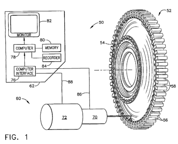
[0009] Figure 1 is a schematic diagram of an exemplary eddy current
surface flaw detection system;
[0010] Figure 2 is a schematic diagram of an exemplary eddy current
array probe;
[0011] Figure. 3 is a block diagram illustrating an exemplary layout
of a calibration block;
[0012] Figure 4 is a plan view of an exemplary component that
includes a plurality of exemplary defects that may be detected during an EC
inspection;
[0013] Figure 5 is an exemplary flow chart of an automated defect
recognition (ADR) process for use with an omni-directional EC array probe;
[0014] Figure 6 is an exemplary plot of output data that corresponds
to a circumferential defect detected using an omni-directional EC probe;
[0015] Figure 7 is an exemplary plot of output data that corresponds
to a radial defect detected using an omni-directional EC probe; and
[0016] Figure 8 is a graphical representation of exemplary data
obtained from a sample including a defect, a plot of a raw test image, a plot
of the raw
test image after compensation, and a plot of the raw test image after
compensation, as
compared to a threshold value.
DETAILED DESCRIPTION OF THE INVENTION
[0017] In one embodiment, an automated defect recognition (ADR)
process for a Wide Area Standard Probe (WASP) is described herein. The WASP is
a
type of eddy current inspection probe that facilitates an efficient and
productive
inspection process through the use of a multi-element scan. A unique advantage
of
-3-
CA 02711129 2010-06-28
WO 2009/083995 PCT/IN2007/000609
the WASP is its ability to detect flaws in substantially any orientation, such
that a
limited amount of data is obtained in comparison to other known eddy current
probes.
However, the benefits gained through the acquisition of a limited amount of
data, may
be offset by the reliability of inspections completed with such probes.
[0018] In an exemplary embodiment, the ADR process automates the
entire data processing procedure. The ADR method also facilitates reliable
flaw
recognition and characterization, while minimizing false defect
identification. In the
exemplary embodiment, signal processing algorithms are used to identify
potential
defect signals from the WASP inspection data and to estimate the size and
orientation
of the defects. The algorithms establish criteria used to estimate the
orientation of the
defect and to apply appropriate corrections in order to facilitate maximizing
the
response from the defect. In addition, the algorithms may function without the
use of
reference images, look-up-tables, or any other a priori information.
[0019] Figure 1 is a schematic diagram of an exemplary eddy current
flaw detection system 50 that may be used to inspect a component 52 such as,
but not
limited to, a gas turbine engine disk 54. In the exemplary embodiment, disk 54
includes a plurality of dovetail posts 56 and a plurality of circumferentially-
spaced
dovetail slots 58 defined between adjacent pairs of posts 56.
[0020] Although the methods and apparatus herein are described
with respect to posts 56 and dovetail slots 58, it should be appreciated that
the
methods and apparatus can be applied to a wide variety of components. For
example,
the present invention may be used with component 52 of any operable shape,
size,
and/or configuration. Examples of such components may include, but are not
limited
to only including, components of gas turbine engines such as seals, flanges,
turbine
blades, turbine vanes, and/or flanges. The component may be fabricated of any
base
material such as, but not limited to, nickel-base alloys, cobalt-base alloys,
titanium-
base alloys, iron-base alloys, and/or aluminum-base alloys. More specifically,
although the methods and apparatus herein are described with respect to
aircraft
engine components, it should be appreciated that the methods and apparatus can
be
-4-
CA 02711129 2010-06-28
WO 2009/083995 PCT/IN2007/000609
applied to, or used to inspect, a wide variety of components used within a
steam
turbine, a nuclear power plant, an automotive engine, or any other mechanical
components.
[0021] In the exemplary embodiment, detection system 50 includes a
probe assembly 60 and a data acquisition/control system 62. Probe assembly 60
includes an eddy current (EC) coil/probe 70 and a probe manipulator 72 that is
coupled to probe 70. Eddy current probe 70 and probe manipulator 72 are each
electrically coupled to data acquisition/control system 62 such that
control/data
information can be transmitted to/from EC probe 70 and/or probe manipulator 72
and/or data acquisition/control system 62. In an alternative embodiment,
system 50
also includes a turntable (not shown) that selectively rotates component 52
during the
inspection procedure.
[0022] Data acquisition/control system 62 includes a computer
interface 76, a computer 78, such as a personal computer with a memory 80, and
a
monitor 82. Computer 78 executes instructions stored in firmware (not shown),
and is
programmed to perform functions described herein. As used herein, the term
"computer" is not limited to just those integrated circuits referred to in the
art as
computers, but rather broadly refers to computers, processors,
microcontrollers,
microcomputers, programmable logic controllers, application specific
integrated
circuits, and other programmable circuits, and these terms are used
interchangeably
herein.
[0023] Memory 80 is intended to represent one or more volatile
and/or nonvolatile storage facilities that shall be familiar to those skilled
in the art.
Examples of such storage facilities often used with computer 78 include, but
are not
limited to, solid-state memory (e.g., random access memory (RAM), read-only
memory (ROM), and flash memory), magnetic storage devices (e.g., floppy disks
and
hard disks), and/or optical storage devices (e.g., CD-ROM, CD-RW, and DVD).
Memory 80 may be internal to, or external from, computer 78. Data
acquisition/control system 62 also includes a recording device 84 such as, but
not
-5-
CA 02711129 2010-06-28
WO 2009/083995 PCT/IN2007/000609
limited to, a strip chart recorder, a C-scan, and/or an electronic recorder
that is
electrically coupled to either computer 78 and/or eddy current probe 70.
[0024] In use, a component 52, such as disk 54, is mounted on a
fixture (not shown) that secures the component 52 in place during inspection.
Eddy
current probe 70 is selectively positioned within dovetail slots 58 to
facilitate enabling
substantially all of the interior of dovetail slots 58 to be scanned during
inspection. In
the exemplary embodiment, probe manipulator 72 is a six-axis manipulator. EC
probe 70 generates electrical signals in response to the eddy currents induced
within
the surface of dovetail slots 58 during scanning of dovetail, slots 58 by
probe 70.
Electrical signals generated by EC probe 70 are received by data
acquisition/control
system 62 via a data communications link 86 and are stored in memory 80 and/or
recorder 84. Computer 78 is also coupled to probe manipulator 72 by a
communications link 88 to facilitate controlling the scanning of disk 54. A
keyboard
(not shown) is electrically coupled to computer 78 to facilitate operator
control of the
inspection of disk 54. In the exemplary embodiment, a printer (not shown) may
be
provided to generate hard copies of the images generated by computer 78.
[0025] In the exemplary embodiment, system 50 may be used to
perform any kind of eddy current inspection, such as conventional inspection,
single-
coil inspection, or array probe inspection. System 50 automatically scans the
surface
of component 52 and stores the acquired data in the form of images. The defect
recognition algorithms will then be employed by computer 78 to identify and
characterize any flaw (if present) on the surface of component 52.
[0026] When an eddy current (EC) test is performed, a magnetic
field is generated by a drive coil. Such generation may include, but is not
limited to
only, supplying an alternating current to a drive coil. The drive coil is
positioned
adjacent to a surface of a component to be tested. When the drive coil is
positioned,
the drive coil is oriented substantially parallel to the surface being tested.
Such an
orientation of the drive coil causes the magnetic field generated by the drive
coil to be
oriented substantially normal to the surface being tested.
-6-
CA 02711129 2010-06-28
WO 2009/083995 PCT/IN2007/000609
[0027] A sensor is coupled to the drive coil to receive secondary
fields. Secondary fields of interest are received at the sensor after the
magnetic fields
generated by the drive coil are reflected from a surface flaw on, or in, the
surface
being tested. The sensor is configured to convert the reflected secondary
field into an
electric signal that may be viewed and/or recorded.
[0028] Figure 2 illustrates an exemplary embodiment of an omni-
directional eddy current (EC) probe 130. Omni-directional EC probe 130
includes at
least one EC channel 132. In the exemplary embodiment, EC channel 132 includes
a
first sense coil 134 and a second sense coil 136. First and second sense coils
134 and
136 are offset from one another in a first (X) and a second (Y) direction and
overlap
one another in at least one of the first and second directions (X,Y). As used
herein,
the terms "offset" and "overlap" are not mutually exclusive. For example, in
the
exemplary embodiment, first and second sense coils 134 and 136 are both offset
and
overlap in the Y direction. In other words, for this orientation, first and
second sense
coils 134 and 136 are partially offset in the (Y) direction, whereas they are
completely
offset (i.e., with no overlap) in the (X) direction. In one embodiment, first
and second
sense coils 134 and 136 overlap in second direction (Y) by at least about
twenty-five
percent (25%) of a length 140 of the sense coils 134 and 136. In another
embodiment,
the first and second sense coils 134 and 136 overlap in the second direction
(Y) by at
least about thirty-three percent (33%) of the length 140 of sense coils 134
and 136. In
another embodiment, first and second sense coils 134 and 136 overlap in second
direction (Y) by at least about fifty percent (50%) of length 140 of sense
coils 134 and
136.
[0029] Omni-directional EC probe 130 also includes at least one
drive coil 138 that generates a probing field for EC channel 132 in a vicinity
of first
and second sensing coils 134 and 136. In the exemplary embodiment, drive coil
138
extends around first and second sense coils 134 and 136 and forms EC channel
132.
[0030] To enhance scanning of a relatively large surface area, an
array of EC channels 132 is employed. Accordingly, the exemplary omni-
directional
-7-
CA 02711129 2010-06-28
WO 2009/083995 PCT/IN2007/000609
EC probe 130 includes a number of EC channels 132 and a number of drive coils
138.
Specifically, in the exemplary embodiment, at least one drive coil 138 is
provided for
each EC channel 132.
[0031] In the exemplary embodiment, the overlapping orientation of
first and second sense coils 134 and 136 enables omni-directional EC probe 130
to
detect imperfections in a sample being tested anywhere along the (Y)
direction.
However, omni-directional EC probe 130 may include any orientation of EC
channels
132 that enables EC probe 130 to function as described herein. By including a
plurality of EC channels 132 that are substantially identical, performance of
the
plurality of EC channels 132 is facilitated to be substantially uniform.
[0032] As described above with respect to EC, probe 70, omni-
directional EC array probe 130 is used to detect surface, or near surface,
cracks (i.e.,
surface connected flaws) in conductive components, such as, but not limited
to,
aircraft engine components including disks, spools, and blades. Exemplary
components are formed of nickel alloys and titanium alloys. However, EC probe
130
may be used with a variety of conductive components.
[0033] Operationally, drive coil 138 excites and generates a magnetic
flux (i.e., probing field). The magnetic field influx into a conductive test
object (not
shown in Figure 1) generates an eddy current on the surface of the test
object, which
in turn generates a secondary magnetic field. In case of a surface flaw (not
shown),
the secondary magnetic field deviates from its normal orientation, to a
direction
corresponding to the flaw orientation. This deviated secondary magnetic field
induces
corresponding signals (i.e., sense signals) in the sense coils 134 and 136
which are
indicative of the presence of the surface flaw. In the exemplary embodiment,
because
of the offset in two directions (i.e., X and Y directions), the differential
coupling of
sense coils 134 and 136 enables the directional deviation in the secondary
magnetic
flux corresponding to any crack orientation to be detected. More specifically,
sense
coils 134 and 136 impart an omni-directional sensitivity to EC probe 130. In
addition,
the overlap orientation of sense coils 134 and 136 in the Y direction
facilitates
-8-
CA 02711129 2010-06-28
WO 2009/083995 PCT/IN2007/000609
complementary sensing while scanning the surface of a test object with the
probe in
the X direction.
[0034] In the exemplary embodiment, first sense coil 134 has a
positive polarity and second sense coil 136 has a negative polarity. The
exemplary
omni-directional EC probe 130 also includes electrical connections 142 that
electrically couple first and second sense coils 134 and 136 together. In one
embodiment, the electrical connections 142 are configured to perform both
differential sensing (indicated by "DIFF") and absolute sensing (indicated by
"ABS").
Beneficially, the inclusion of both differential and absolute sensing features
facilitates
the detection of both small and long cracks.
[0035] First and second sense coils 134 and 136 form each EC
channel 132 and have opposite polarity (indicated by "+" and "-"), and
electrical
connections 142 electrically couple first and second sense coils 134 and 136
within
each respective EC channel 132. Drive coils 138 have alternating polarity with
respect to adjacent drive coils 138 (also indicated by "+" and "-"). The
polarity of
first and second sense coils 134 and 136 alternates correspondingly with
respect to
adjacent EC channels. For example, those sense coils 134 and 136 within the
middle
EC channel 132 have the opposite polarity relative to those sense coils 134
and 136 in
the upper and lower EC channels 132.
[0036] In an alternative embodiment, each EC channel 132 includes
a sensor. For example, in one embodiment, the sensor is a solid-state sensor,
such as,
but not limited to, a Hall sensor, an anisotropic magnetic resistor (AMR), a
giant
magnetic resistor (GMR), a tunneling magnetic resistor (TMR), an extraordinary
magnetoresistor (EMR), and/or a giant magnetoimpedance (GMI). However, any
unpackaged solid-state sensor that enables eddy current testing as described
herein
may be used.
[0037] Figure 3 is a block diagram illustrating an exemplary layout a
calibration block 200 that may be used to calibrate an omni-directional EC
array
probe, for example, omni-directional EC array probe 240. In one embodiment, EC
-9-
CA 02711129 2010-06-28
WO 2009/083995 PCT/IN2007/000609
array probe 240 is substantially similar to EC array probe 130 (shown in
Figure 2). In
the exemplary embodiment, calibration block 200 includes a first edge 202, and
a
second edge 204, and a plurality of test notches 210. More specifically, in
the
exemplary embodiment, the plurality of test notches 210 include multiple rows
of test
notches. For example, in the exemplary embodiment, test notches 210 include a
first
row of notches 212, a second row of notches 214, a third row of notches 216,
and a
fourth row of notches 218. Each row 212, 214, 216, and 218 includes a
plurality of
individual notches. More specifically, in the exemplary embodiment, each row
212,
214, 216, and 218 includes a first notch 220 positioned adjacent first edge
202. Each
row 212, 214, 216, and 218 also includes a second notch 222 positioned a
predetermined distance 224 in the Y direction from first notch 220, and a
third notch
226 positioned a predetermined distance 228 in the 'Y direction from second
notch
222. The placement of the notches ensures that consistent reference voltage is
obtained, regardless of where probe coils are located at different notches.
[0038] An omni-directional EC array probe 240 is initially positioned
on calibration block 200. Probe 240 is then calibrated by moving probe 240
relative
to calibration block 200 while measuring a voltage detected by the sensing
coils
(shown in Figure 2) as the sensing coils pass over notches 210. Specifically,
the
detected voltage is measured at each notch 210. With the detected voltages, a
single
instrument gain is set based on the maximum notch response, independent of EC
channel (shown in Figure 2). Once the gain is set, normalization factors are
used to
insure a uniform response across the sensing coils. The calculated gain
settings
produced with calibration block 200 facilitate increasing the accuracy of the
acquired
data when compared to a non-calibrated EC array probe.
[0039] Figure 4 is a plan view of an exemplary component 250 that
includes a plurality of exemplary defects. For example, in the exemplary
embodiment, component 250 includes a radial defect 260, a circumferential
defect
262, and an angled defect 264. Radial defect 260, circumferential defect 262,
and
angled defect 264 are examples of different defect orientations that may occur
within
component 250. An exemplary EC probe path is illustrated at 266. As described
in
-10-
CA 02711129 2010-06-28
WO 2009/083995 PCT/IN2007/000609
more detail below, radial defect 260, circumferential defect 262, and angled
defect
264 respond differently to EC array probe 240, in terms of a maximum amplitude
of
the response and a signature of the response.
[0040] Figure 5 is an exemplary flow chart of an automated defect
recognition (ADR) process 280 that may be used with an omni-directional EC
array
probe, such as EC array probe 240 (shown in Figure 3). In an exemplary
embodiment, ADR process 280 is performed via a processing device (not shown in
Figure 5). As used herein, the term "processing device" is not limited to just
those
integrated circuits referred to in the art as a processing device, but broadly
refers to, a
processor, a microprocessor, a controller, a microcontroller, a programmable
logic
controller, an application specific integrated circuit, and other programmable
circuits.
ADR process 280 facilitates accurate flaw recognition and characterization
while
limiting false identifications of defects. In one embodiment, ADR process 280
is
performed by EC flaw detection system 50 (shown in Figure 1). ADR process 280
includes calibrating 282 the EC array probe. The response of the EC array
probe to a
defect varies depending on the location of the EC array probe that senses the
defect.
Calibrating 282 may include determining a probe gain that provides a
consistent
response of detected defects across the EC array probe. Moreover, calibrating
282
may be accomplished using a calibration block, such as, calibration block 200
(shown
in Figure 3), for example.
[0041] ADR, process 280 also performs 284 an EC test of the
component and produces a test image (not shown in Figure 5). The test image
produced represents a plot of detected voltages over a distance or location of
the EC
array probe relative to the component surface. Processing 286 the test image
produces a processed test image (not shown in Figure 5). In the exemplary
embodiment, during processing 286, a wavelet decomposition is used to
facilitate
improving small crack detection, and improving the probability of detection
(PoD).
PoD is a measurement of, for example, the ability of a non-destructive test to
identify
an imperfection of a known size within a component.
-11-
CA 02711129 2010-06-28
WO 2009/083995 PCT/IN2007/000609
[0042] More specifically, in the exemplary embodiment, an
algorithm decomposes the raw test image into various frequency sub-bands in
the
wavelet domain. The sub-bands are then subjected to a plurality of noise
filters and
adaptive thresholds, that are customized to the signal content of the sub-band
under
consideration. The use of appropriate sub-bands enhances the flaw response
signature
and thereby facilitates improving detectability and reducing the possibilities
of false
positives as compared to applying conventional rigid threshold segmentation
schemes
on the raw test data. ADR process 280 also includes compensating 288 the
processed
test image to correct for various signal levels detected, depending on the
geometry of
the detected defect.
[0043] ADR process 280 also includes calculating 290 an estimation
of the size of a detected defect. The estimation of the size of the detected
defect is
based on the processed test image after compensating 288 which provides for
higher
accuracy of the size estimate while limiting false indications of a defect.
The
estimation of the size of the detected defect is then compared to a threshold
value. If
the estimated size of the detected defect is higher than the threshold value,
a defect is
noted. If the estimation of the size of the detected defect is lower than the
threshold
value, no defect is noted. Threshold values are calculated by PoD analysis.
[0044] Figure 6 is a plot 300 of an exemplary data output from an
exemplary omni-directional EC probe, such as EC array probe 240 (shown in
Figure
3). Specifically, plot 300 includes a plot 304 of a first peak-to-peak voltage
(Vpp), a
plot 306 of a second Vpp, and a plot 308 of a third Vpp. First plot 304,
second plot
306, and third plot 308 illustrate an output of an omni-directional EC probe
as the
probe detects a circumferential defect 262 (shown in Figure 4). In the
exemplary
embodiment, three coils are used to detect circumferential defect 262, and to
collect
output data to produce first plot 304, second plot 306, and third plot 308.
[0045] In the exemplary embodiment, compensating 288 (shown in
Figure 5) the processed test image to correct for the various signal levels
detected
includes calculating a maximum Vpp 310 from first plot 304, second plot 306,
and
-12-
CA 02711129 2010-06-28
WO 2009/083995 PCT/IN2007/000609
third plot 308 when the test image indicates the presence of a circumferential
defect.
Maximum Vpp 310 enables a maximum response to be extracted from the data
provided by the omni-directional EC probe.
[0046] Figure 7 is an exemplary plot 340 of exemplary data output
from an exemplary omni-directional EC probe, such as probe 240 (shown in
Figure
3). Plot 340 includes a plot 344 of a first Vpp, a plot 346 of a second Vpp,
and a plot
348 of a third Vpp. First plot 344, second plot 346, and third plot 348
illustrate an
output of an omni-directional EC probe as the probe detects a radial defect
260
(shown in Figure 4). In the exemplary embodiment, three coils are used to
detect
radial defect 260, and to collect output data to produce first plot 344,
second plot 346,
and third plot 348.
[0047] In the exemplary embodiment, compensating 288 (shown in
Figure 5) the processed test image to correct for the various signal levels
detected
includes calculating a sum 350 from first plot 344, second plot 346, and third
plot 348
when the test image indicates the presence of a radial defect. Sum 350 enables
a
maximum response to be extracted from the data provided by the omni-
directional EC
probe.
[0048] Compensating 288 corrects partial defect responses, such as,
for example, plot 344 of first Vpp, plot 346 of second Vpp, and plot 348 of
third Vpp,
so as to produce one single maximum defect response, for example, maximum Vpp
310 and sum 350. As described above, maximum Vpp 310 and sum 350 are used to
predict the size of the defect.
[0049] Figure 8 is a graphical illustration of a component to be tested
370 including a defect 372, a plot 380 of a raw test image, a plot 390 of the
raw test
image after compensation, and a plot 400 of the raw test image after
compensation
and comparison to a threshold value. In an exemplary embodiment, plot 380 is
created from data obtained by omni-directional EC array probe 240. Plot 380
shows
voltage levels detected as an EC array probe (not shown in Figure 8) moves
across
component 370. Plot 390 is produced after compensation 288 is applied
(described
-13-
CA 02711129 2010-06-28
WO 2009/083995 PCT/IN2007/000609
above with respect to Figure 5) to the raw test image of plot 380 by a
processing
device (not shown in Figure 8). In the exemplary embodiments, after
compensation
for the possible defect orientations is performed as described above, a first
area of
interest 392 and a second area of interest 394 are apparent. Once the data
forming
plot 390 is compared to the calculated threshold value corresponding to a
predetermined PoD, first area of interest 392 is no longer identified as a
potential
component defect. In plot 400, only second area of interest 394 remains, which
corresponds to the only defect 372 present in component 370.
[0050] In summary, the ADR process described herein facilitates the
identification and segmentation of the flaw responses amidst various forms of
electronic noise and part geometry indications using an adaptive thresholding
scheme.
Flaws of different orientations respond differently to the WASP array, both in
terms
of maximum amplitude of the response and in terms of its signature. The ADR
process performs a compensation of image data corresponding to various flaw
orientations to facilitate maximizing the extracted probe response. Once
segmented,
the flaw orientation is estimated in order to extract the appropriate maximum
response.
[0051] As described above, the ADR process does not require prior
information in the form of look-up tables, threshold values, or reference
images. The
image processing with the use of the wavelet decomposition has improved small
crack
detection, which facilitates improved PoD. The algorithm decomposes the image
into
various frequency sub-bands in the wavelet domain. The sub-bands are then
subjected to a cascade of noise filters and adaptive thresholds, which are
customized
to the signal content of the sub-band under consideration. The use of
appropriate sub-
bands offers the advantage of enhancing the flaw response signature, while not
simultaneously enhancing a level of noise, thereby facilitating improving a
signal to
noise ratio (SNR), detestability, and reducing the possibilities of false
positives. This
provides improvement over the conventional rigid threshold segmentation
schemes on
the raw data.
-14-
CA 02711129 2010-06-28
WO 2009/083995 PCT/IN2007/000609
[0052] The compensation schemes apart from maximizing flaw
responses, can estimate orientation of the flaw segmented. The peak-to-peak
response
is calculated for each region. Based on the orientation, the appropriate
compensation
is applied to facilitate deriving a maximum flaw response.
[0053] Improved defect characterization capability has been achieved
by using a multivariate linear transformation to predict equivalent defect
size. The
multivariate equation is derived from regression analyses of various features
extracted
from the segmented region. The features used include maximum amplitude, number
and polarity of peaks, energy of the segment and other derived features. Based
on
these features a transfer function has been developed that directly predicts
the
equivalent size of the detected defect.
[0054] By providing small flaw detection ability and reduced false
positives, ADR process consequently improves the PoD. Use of the appropriate
wavelet facilitates enhancing the flaw signature, while suppressing noise.
Reductions
in false identification of defects directly impact the First Time Yield (FTY)
of the
inspection. A poor FTY can negate any advantages WASP might provide in terms
of
inspection time.
[0055] Exemplary embodiments of eddy current inspection processes
and systems are described above in detail. The processes and systems are not
limited
to the specific embodiments described herein, but rather, components of each
system
may be utilized independently and separately from other components described
herein. Each system component can also be used in combination with other
system
components. More specifically, although the processes and systems herein are
described with respect to inspection of aircraft engine components, it should
be
appreciated that the processes and systems can also be applied to a wide
variety of
components used within a steam turbine, a nuclear power plant, an automotive
engine,
or to inspect any mechanical component.
-15-
CA 02711129 2010-06-28
WO 2009/083995 PCT/IN2007/000609
[0056] While the invention has been described in terms of various
specific embodiments, those skilled in the art will recognize that the
invention can be
practiced with modification within the spirit and scope of the claims.
-16-