Note: Descriptions are shown in the official language in which they were submitted.
CA 02711459 2015-09-08
4
WAVELENGTH DIVISION MULTIPLEXING MODULE
Field
The present disclosure generally relates to fiber optic telecommunications
equipment.
More specifically, the present disclosure relates to modules for housing fiber
optic
telecommunications equipment.
Background
In fiber optic telecommunications systems, it is common for optical fibers of
transmission cables to be split into multiple strands, either by optical
splitting of a signal
carried by a single stranded cable or by fanning out the individual fibers of
a multi-strand
cable. Further, when such systems are installed, it is known to provide excess
capacity in the
installations to support future growth and utilization of the fibers. Often in
these installations,
modules including splitters or fanouts are used to provide the connection
between
transmission fibers and customer fibers. To reduce the cost and complexity of
the initial
installation and still provide options for future expansion, a module mounting
chassis capable
of mounting multiple modules may be used in such an installation.
While a chassis may accept several modules, the initial installation may only
include fewer modules mounted in the chassis, or enough to serve current
needs.
These chassis may be configured with limited access to one or more sides, or
may be
mounted in cramped locations. In addition, some of these chassis may be pre-
configured with the maximum capacity of transmission cables to accommodate and
link to modules which may be installed in the future. Since it is desirable to
have
access to components within the chassis for cleaning during the installation
of a
1
CA 02711459 2010-07-06
WO 2009/097388 PCT/US2009/032349
new module, some provision or feature of the chassis will desirably permit a
user to
access and clean the connectors of these pre-connectorized and pre-installed
transmission cables.
It is also desirable for the chassis to be configured to ensure that
modules are installed correctly and aligned with other components within the
chassis
to mate with the pre-connectorized and pre-installed transmission cables.
In fiber-optic communications, it is also common for optical signals
of transmission cables to be multiplexed. Wavelength division multiplexing
(WDM) is a technology which multiplexes multiple optical carrier signals on a
single optical fiber by using different wavelengths of laser light to carry
different
signals. This allows for a multiplication in capacity, in addition to making
it
possible to perform bidirectional communications over one strand of fiber.
A WDM system uses a multiplexer at the transmitter to join signals
together and a demultiplexer at the receiver to split them apart. With the
right type
of fiber, it is possible to have a device that does both simultaneously, and
can
function as an optical add-drop multiplexer. WDM systems allow expansion of
the
capacity of the network without laying more fiber.
WDM systems are divided in different wavelength patterns: 1)
conventional WDM; 2) dense WDM (DWDM); and 3) coarse WDM (CWDM).
WDM, DWDM and CWDM are based on the same concept of using multiple
wavelengths of light on a single fiber, but differ in the spacing of the
wavelengths,
number of channels, and the ability to amplify the multiplexed signals in the
optical
space.
In certain telecommunications applications, it might be desirable to
combine wavelength division multiplexing technology with fiber optic signal
splitting technology.
Summary
The present invention relates to telecommunications equipment that
combines wavelength division multiplexing technology and fiber optic signal
splitting technology and packages it in a modular format. The module of the
present
disclosure includes an input for inputting a fiber optic signal to be split
into multiple
strands, an input for inputting a fiber optic signal to be demultiplexed into
different
wavelengths of laserlight, and an output for outputting a combination signal
wherein
2
CA 02711459 2015-09-08
a split signal and a demultiplexed wavelength are combined into a single
output fiber.
According to one aspect of the invention, there is provided a
telecommunications
module comprising:
a housing defining an interior and including a first sidewall, a second
sidewall, a top
wall, a bottom wall, a rear wall, and a front wall, the housing extending in a
longitudinal
direction from the front wall toward the rear wall;
a first module input location positioned adjacent the front wall of the
housing and a
second module input location positioned adjacent the front wall of the
housing;
a module output location positioned adjacent the front wall of the housing;
an optical wavelength division multiplexer/demultiplexer mounted within the
interior
of the housing and having a multiplexer length extending generally parallel to
the longitudinal
direction of the housing, the optical wavelength division
multiplexer/demultiplexer including a
multiplexer input location facing toward the rear wall and a multiplexer
output location facing
toward the front wall, the optical wavelength division
multiplexer/demultiplexer configured to
demultiplex an optical signal input into the telecommunications module via the
first module
input location into a plurality of different wavelengths;
a fiber optic splitter mounted within the interior of the housing and having a
splitter
length extending generally parallel to the longitudinal direction of the
housing, the fiber optic
splitter including a splitter input location facing toward the front wall and
a splitter output
location facing the rear wall, the fiber optic splitter configured to split an
optical signal input
into the telecommunication module via the second module input location into a
plurality of
signals; and
a plurality of optical add/drop filters mounted within the interior of the
housing, each
of the optical add/drop filters having a filter length extending generally
parallel to the
longitudinal direction of the housing, each of the optical add/drop filters
configured to
combine one of the signals that has been split by the fiber optic splitter and
one of the
wavelengths that has been demultiplexed by the optical wavelength division
multiplexer/demultiplexer into a combination output signal that is output by
the
telecommunications module through the module output location, each optical
add/drop filter
3
CA 02711459 2015-09-08
including a first filter input location facing toward the front wall, a second
filter input location
facing toward the rear wall, and a filter output location facing toward the
rear wall, the first
filter input location configured to receive a signal from the fiber optic
splitter and the second
filter input location configured to receive a signal from the optical
wavelength division
multiplexer/demultiplexer.
Brief Description of the Drawings
The accompanying drawings, which are incorporated in and constitute a part of
the
description, illustrate several aspects of the inventive features and together
with the detailed
description, serve to explain the principles of the disclosure. A brief
description of the drawings
is as follows:
FIG. 1 is an exploded view of a fiber optic wavelength-division multiplexing
(WDM)
module having features that are examples of inventive aspects in accordance
with the present
disclosure;
FIG. 2 illustrates the WDM module of FIG. 1 in a fully assembled configuration
including
the input and the output signals going into and a coming out of, respectively,
the module;
FIG. 3 is a right side view of the WDM module of FIG. 1;
FIG. 4 is a left side view of the WDM module of FIG. 1;
FIG. 5 is an exploded view of a module housing of the WDM module of FIG. 1;
FIG. 6 is a perspective view of a splice holder/cable management structure of
the WDM
module of FIG. 1;
FIG. 7 is a bottom view of the splice holder/cable management structure of
FIG. 6;
FIG. 8 is a front view of the splice holder/cable management structure of FIG.
6;
FIG. 9 is a perspective view of another cable management structure of the WDM
module of FIG. 1;
FIG. 10 is a top view of the cable management structure of FIG. 9;
FIG. 11 is a front view of the cable management structure of FIG. 9;
FIG. 12 is a schematic view illustrating the fiber optic circuit of the WDM
module of
FIG. 1;
3a
CA 02711459 2010-07-06
WO 2009/097388
PCT/US2009/032349
FIG. 13 is a diagram illustrating a fiber optic splitter configured for
use in the WDM module of FIG. 1;
FIG. 14 is a diagram illustrating a multiplexer chip configured for use
in the WDM module of FIG. 1;
FIG. 15 is a diagram illustrating an optical add/drop filter configured
for use in the WDM module of FIG. 1, the add/drop filter configured to combine
a
split signal and a demultiplexed wavelength into a single output fiber;
FIG. 16 is an exploded view of an input connection for inputting a
signal into the splitter of the WDM module of FIG. 1;
FIG. 17 illustrates the input connection of FIG. 16 in a fully
assembled configuration;
FIG. 18 illustrates an input connection in a fully assembled
configuration for inputting a signal into the multiplexer chip of the WDM
module to
be demultiplexed into different wavelengths of laserlight;
FIG. 19 is a diagram illustrating the input connection of FIG. 17 with
the fiber optic circuit of the fiber optic splitter configured for use with
the WDM
module;
FIG. 20 is a diagram illustrating the input connection of FIG. 18 with
the fiber optic circuit of the multiplexer chip configured for use with the
WDM
module;
FIG. 21 is an exploded view of an output connection for outputting a
signal from the WDM module of FIG. 1;
FIG. 22 illustrates the output connection of FIG. 21 in a fully
assembled configuration;
FIG. 23 illustrates an example routing of a fiber optic cable from an
input connection of the WDM module to an input location of the fiber optic
splitter
within the WDM module;
FIG. 24 illustrates an example routing of a fiber optic cable from an
output location of the fiber optic splitter to an input location of an optical
add/drop
filter that is configured to combine a split signal and a demultiplexed
wavelength
into a single output fiber;
FIG. 25 illustrates an example routing of a fiber optic cable from an
input connection of the WDM module to an input location of the multiplexer
chip
within the WDM module;
4
CA 02711459 2015-09-08
FIG. 26 illustrates an example routing of a fiber optic cable from an output
location of
the multiplexer chip to an input location of an optical add/drop filter that
is configured to
combine a split signal and a demultiplexed wavelength into a single output
fiber;
FIG. 27 illustrates an example routing of a fiber optic cable from an output
location of
the optical add/drop filter that is configured to combine a split signal and a
demultiplexed
wavelength to an output connection of the WDM module; and
FIG. 28 is a diagram illustrating an example positioning of a plurality of
output
connections of the WDM module among a plurality of filler crimp tubes.
Detailed Description
Reference will now be made in detail to exemplary aspects of the present
disclosure
which are illustrated in the accompanying drawings. Wherever possible, the
same reference
numbers will be used throughout the drawings to refer to the same or similar
parts.
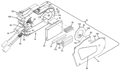
FIGS. 1-4 illustrate a telecommunications module 10 having features that are
examples
of inventive aspects in accordance with the present disclosure. Since one of
the
telecommunications equipment housed by the module 10 is a fiber optic
wavelength division
multiplexer/demultiplexer, the telecommunications module 10 may also be
referred to herein
as a fiber optic wavelength division multiplexing (WDM) module 10. The WDM
module 10 is
configured to be inserted within a telecommunications chassis similar to the
chassis shown and
described in commonly-owned U.S. Patent Application Ser. No. 11/975,905 (filed
October 22,
2007, entitled WAVELENGTH DIVISION MULTIPLEXING MODULE, now US Patent No.
7,536,075). As will be described in further detail below, the WDM module 10 is
also configured
to be inserted into the telecommunications chassis in a similar manner to that
shown and
described in the U.S. Patent Application Ser. No. 11/975,905.
The WDM module 10 of the present disclosure is configured to power split an
input signal into a plurality of signals. The WDM module 10 is also configured
to
demultiplex a second input signal into a plurality of wavelengths. An optical
device
22 (e.g., an optical add/drop filter, a single channel filter, etc.) within
the module 10
is configured to combine one of the power split signals and one of the
5
CA 02711459 2010-07-06
WO 2009/097388 PCT/US2009/032349
demultiplexed wavelengths into a combination output signal that is output
through
the module 10. The powersplitting function, the demultiplexing function and
the
signal combination function are all performed within the module 10.
Referring to FIG. 1, the WDM module 10 is shown in an exploded
orientation. WDM module 10 includes a module housing 12 that includes a main
housing portion 14 and a removable cover 16. The module housing 12 including
the
main housing portion 14 and the removable cover 16 is illustrated separately
in FIG.
5, without the internal components of the module 10.
Still referring to FIG. 1, the WDM module 10 is configured to house
a fiber optic splitter 18, a multiplexer/demultiplexer chip 20, and a
plurality of
optical devices 22 configured to combine a split signal and a demultiplexed
wavelength into a single output signal. According to one embodiment, the
optical
devices 22 that are configured to combine a split signal and a demultiplexed
wavelength into a single output signal may be optical add/drop filters.
Optical
add/drop filters and their uses are known in the art. The optical add/drop
filters may
also be called single channel filters. Other types of devices performing the
same
function are possible.
The fiber optic splitter 18 is adapted to power split a first input fiber
optic signal entering the module 10 into multiple strands. The
multiplexer/demultiplexer chip 20 is configured to demultiplex a second input
fiber
optic signal entering the module 10 into different wavelengths of laserlight.
Each of
the optical devices 22 (e.g., add/drop filters) is configured to combine one
of the
split signals and one of the demultiplexed wavelengths into a single output
fiber.
Each of the combination signals are then output from the module 10. In the
embodiment shown, the fiber optic splitter 18 is a 1x8 splitter and the
multiplexer/demultiplexer 20 is an 8-channel chip. Accordingly, in the
embodiment
of the module 10 shown, 1 splitter input signal and 1 multiplexer input signal
get
output as 8 separate combination signals.
A fiber optic circuit diagram of the WDM module 10 of FIGS. 1-4 is
shown in FIG. 12. FIG. 13 diagrammatically illustrates the fiber optic
splitter 18
configured for use in the WDM module 10. FIG. 14 diagrammatically illustrates
the
multiplexer chip 20 configured for use in the WDM module 10. FIG. 15
diagrammatically illustrates one of the add/drop filters 22 configured for use
in the
6
CA 02711459 2010-07-06
WO 2009/097388 PCT/US2009/032349
=
WDM module 10 of FIG. 1, wherein the add/drop filter 22 is configured to
combine
a split signal and a demultiplexed wavelength into an output signal.
According to one example embodiment shown in FIG. 12, a signal
input into the fiber optic splitter 18 gets split into 8 separate signals,
each separate
signal being the same as the original input signal. It should be noted that in
other
embodiments, the fiber optic splitter 18 may power split the signal into
different
power levels, rather than into the same signal. From an output 24 of the
splitter 18,
each of the split signals get spliced into an input 26 (i.e., PASS leg) of
each of the
add/drop filters 22. Likewise, a signal input into the multiplexer chip 20
gets
demultiplexed into 8 different wavelengths. Each wavelength gets output from
the
multiplexer chip 20 as a separate signal and is spliced into another input 28
(i.e.,
REF leg) of the each of the add/drop filters 22. The signals from the splitter
18 and
the multiplexer chip 20 are combined at the add/drop filters 22 and output
from the
add/drop filters 22 (e.g., at COM leg) as 8 combination signals.
FIG. 2 illustrates the WDM module 10 with the two input signal
cables 30, 32 going into the module 10 and the eight combination output signal
cables (each one designated as "34") coming out. As shown, the input cables
30, 32
and the output cables 34 may be connectorized and be forwarded on to
appropriate
locations through fiber optic adapters 36. As shown in FIG. 2, the module
housing
12 includes a cable exit 38 for outputting the combination fiber optic signals
out of
the module 10 and to customers.
Referring back to FIG. 1, the WDM module 10 includes a number of
cable management/routing features for correctly orienting the cables within
the
module 10, as will be described in further detail below. One such feature is a
splice
holder/cable management structure 40 that is configured to house the plurality
of
fiber optic splices 42 within the module 10 and also route fiber optic cables
through
the module 10 (shown in further detail in FIGS. 6-8). Another cable routing
feature
is a cable management structure 44. In the depicted embodiment, the cable
management structure is shown located between the fiber optic splitter 18 and
the
add/drop filters 22 (shown in further detail in FIGS. 9-11). In other
embodiments,
the cable management structure 44 could be located between the fiber optic
splitter
18 and the bottom wall 54 of the module 10. A fiber retainer 46 that is
removably
mounted to the main housing portion 14 of the module housing 12 is also shown
in
7
CA 02711459 2010-07-06
WO 2009/097388
PCT/US2009/032349
FIG. 1. The fiber retainer 46 helps keep cables spooled around a first radius
limiter
48 within the main housing 14 of the module 10.
FIGS. 2-4 illustrate the module 10 in a fully assembled configuration
with the cover 16 mounted on the main housing portion 14.
FIG. 5 illustrates the housing 12 of the module 10 in isolation, with
the internal features of the module 10 removed therefrom. Referring to FIG. 5,
the
main housing portion 14 defines a first sidewall 50 extending between a top
wall 52,
a bottom wall 54, a rear wall 56, and a front wall 58. Removable cover 16
defines a
second sidewall 60 of the module housing 12 and closes off an open side 62 of
the
module main housing portion 14. Cover 16 is mounted to main housing portion 14
by fasteners through fastener holes 64 in the cover 16 and fastener mounts 66
defined on main housing portion 14. The cover 16 may include a label 68 placed
thereon with indicia relating to the module 10 (see FIGS. 1 and 3).
The main housing portion 14 defines a top mounting flange 70 and a
bottom mounting flange 72 of the WDM module 10 extending from the top and
bottom walls 52, 54, respectively. As discussed previously, the WDM module 10
of
the present application is configured for insertion into a chassis similar to
the one
described in U.S. Patent Application Ser. No. 11/975,905 and in a similar
manner to
that described therein. As such, similar to the modules and the chassis
described in
U.S. Patent Application Ser. No. 11/975,905, the bottom flange 72 and a
corresponding slot on the chassis are smaller in size than top flange 70 and
the
corresponding top slot on the chassis. Bottom slot of the chassis is sized
such that,
while bottom flange 72 fits into the bottom slot of the chassis, the larger
top flange
70 does not fit. This ensures that the WDM module 10 is positioned within a
front
opening of a chassis in a particular desired orientation to correctly position
the cable
inputs and the outputs relative to the chassis.
It should also be noted that while the housing 12 of the WDM
module 10 of the present application is configured similarly to those of the
modules
shown in described in U.S. Patent Application Ser. No. 11/975,905 for mounting
purposes, the WDM module 10 of the present application has certain
differences.
The WDM module housing 12 of the present application has the depth of two of
the
modules of U.S. Patent Application Ser. No. 11/975,905. As such, the WDM
module 10 of the present application occupies two mounting locations within a
chassis such as the chassis shown in U.S. Patent Application Ser. No.
11/975,905.
8
CA 02711459 2015-09-08
Still referring to FIG. 5, the rear wall 56 of main housing portion 14
includes a curved
portion 74 configured to provide bend radius protection to cables within
interior of the module
10. Similar to modules of U.S. Patent Application Ser. No. 11/975,905, the
rear wall 56 of main
housing 14 includes an inset portion 76. The inset portion 76 might be used to
accommodate a
pair of fiber optic connectors protruding out of the rear wall 56, if, for
example, a rear input
configuration is desired instead of a front input configuration. It should be
noted that in the
depicted embodiment, the WDM module 10 includes a front input configuration.
Thus, the
slots 78 for receiving fiber optic connectors at the rear wall 56 may be
covered with inserts 80
(see FIG. 5). In U.S. Patent Application Ser. No. 11/975,905, the modules are
shown with a rear
input configuration wherein rear fiber optic connectors protrude from the rear
wall at the inset
portion of the module housing. As noted before, a rear input configuration is
certainly one
option for the WDM module 10 of the present application. In such a
configuration, fiber optic
connectors protruding rearwardly from rear wall 56 would mate with fiber optic
adapters of
adapter assemblies that are mounted within the chassis.
As shown in FIG. 1, in the depicted embodiment, the input connections 82, 84
are
provided at the front of the module main housing 14. FIG. 16 illustrates an
exploded view of an
input connection 82 for inputting a signal into the splitter 18 of the WDM
module 10 and FIG.
17 illustrates the input connection 82 of FIG. 16 in a fully assembled
configuration. FIG. 19 is a
diagram illustrating the input connection 82 with the fiber optic splitter 18
configured for use
in the WDM module 10.
FIG. 18 illustrates a fully assembled view of the input connection 84 for
inputting a
signal into the multiplexer chip 20 of the WDM module 10 to be demultiplexed
into different
wavelengths of laserlight. FIG. 20 is a diagram illustrating the input
connection 84 with the
multiplexer chip 20 configured for use in the WDM module 10.
As shown in FIGS. 16-20, each input connection 82, 84 (whether for the fiber
optic splitter 18 or the multiplexer chip 20) includes a boot 86 that mates
with a
crimp element 88. The crimp element 88 defines a circumferential notch 90
(i.e.,
recessed portion). The circumferential notch 90 is slidably inserted into a
slot 92
defined on an insert piece 59 that is fastened to the front wall 58 of the
main
housing portion 14 with fasteners (see FIGS. 1 and 5). The crimp elements 88
of the
9
CA 02711459 2010-07-06
WO 2009/097388 PCT/US2009/032349
input connections 82, 84 are captured by the cover 16 when the cover 16 is
mounted
on the main housing 14.
As mentioned previously, the embodiment of the WDM module 10
illustrated includes the cable exit 38 at the front of module main housing 14
(see
FIG. 1). The cable exit 38 is slidably mounted to main housing 14 of the WDM
module 10 and is captured by the cover 16 when cover 16 is mounted to main
housing 14. The cable exit 38 defines a protruding rear lip 94 that is
slidably
inserted into a slot 96 defined around a front aperture 98 defined at the
front wall 58
for accommodating the cable exit 38. The cable exit 38 permits
telecommunications
cables within the module 10 to be directed outside of the module 10. The cable
exit
38 is preferably sized to fit within the profile of the WDM module 10 to
preserve the
density of a telecommunications assembly having a plurality of modules 10
mounted
adjacent to each other.
The front wall 58 of the module main housing 14 is angled with
regard to a front opening of a chassis, which may aid in directing cables
entering and
exiting the WDM module 10 toward a desired location. In other embodiments,
front
walls could be made generally parallel to a front of chassis within the scope
of the
present disclosure.
As noted above, the WDM module 10 of the present application
includes similar features to those modules shown and described in U.S. Patent
Application Ser. No. 11/975,905 for mounting purposes. As such, the main
housing
portion 14 includes an integrally formed flexible latch 100 (i.e., cantilever
arm) that
is adapted to engage a portion of a chassis to hold module 10 within a front
opening
of the chassis. Flexible latch 100 also deflects to permit withdrawal of the
module
10 from a chassis. The flexible latch 100 of the module 10 is constructed
similarly
to that of modules of U.S. Patent Application Ser. No. 11/975,905 and includes
a
finger grip tab 102, a front latching tab 104 and a rear latching tab 106 that
cooperate with a bulkhead at a mounting location of a chassis. The WDM module
10 also includes a fixed grip tab 108 opposing and adjacent to flexible latch
100 to
aid removal of module 10 from chassis. Fixed grip tab 108 is preferably
positioned
on module 10 opposite latch 100 so that a user may apply opposing force on
latch
100 and fixed grip tab 108 to securely gasp module 10 and remove it from a
chassis
with two adjacent fingers of the hand. The insertion of the WDM module 10 into
a
CA 02711459 2010-07-06
WO 2009/097388 PCT/US2009/032349
chassis is similar to that of modules described in U.S. Patent Application
Ser. No.
11/975,905.
Now referring back to FIG. 5, within interior of main housing 14,
module includes a first radius limiter 48 adjacent the curved portion 74 of
rear wall
56 of main housing 14. The WDM module 10 includes a second radius limiter 110
adjacent front wall 58 of housing 12 near the cable exit 38. As will be
discussed in
further detail below, the radius limiters 48, 110 provide bend-protection to
fiber
cables within the module 10 while providing cable management/routing
functionality.
Still referring to FIG. 5, the module main housing 14 also includes
integrally formed crimp holders 112 (e.g., slots) adjacent the front wall 58
of
housing 14 underneath the second radius limiter 110. Crimp elements 114 (see
FIGS. 21-22) crimped to the ends of cables that are extending from the output
locations 116 of the add/drop filters 22 are slidably received into the crimp
holders
114. Crimp elements 114 include square flanges 118 between which are defined
recessed portions 120. The crimp holders 112 include complementary structure
to
the crimp elements 114 such that once the crimp elements 114 are slidably
inserted
into the crimp holders 112, the crimp elements 114 are prevented from moving
in a
longitudinal direction due to the flanges 118. Once slidably inserted, crimp
elements 114 are held in place by the cover 16 that is mounted on the module
main
housing 14. The assembly of an output connection 122 for outputting a signal
from
the WDM module 10 is shown in detail in FIGS. 21 and 22. A crimp element 114
is
crimped and terminated to a cable in a manner commonly known in the art.
In the embodiment shown, there are four crimp holding slots 112,
each slot 112 being able to accommodate up to eight crimp elements 114 (see
FIG.
28). Since there are eight combination output signals in the embodiment of the
WDM module 10 shown, the output cables 34 occupy eight crimp holding positions
124. The rest of the positions 124 may be filled with dummy crimp elements or
inserts/fillers that are not connected to cables, making sure the crimp
elements 114
crimped to active output cables 34 do not slide out of the slots 112. In FIG.
28, one
example positioning of a plurality of "active" crimp elements 114 among filler
crimp
elements is shown.
In the embodiment of the module shown, the crimp holders 112
provide the capacity for up to thirty-two crimp elements 114 connected to
output
11
CA 02711459 2010-07-06
WO 2009/097388 PCT/US2009/032349
cables 34. Thus, the WDM module 10 of the present disclosure could house, if
desired, a lx32 fiber optic splitter and a 32 channel multiplexer. Also, the
configuration of the module housing 12 can certainly be modified to
accommodate
other number of inputs or outputs, as desired. In addition, other
complementary
shapes between the crimp elements 114 and the crimp holders 112 are possible
to
provide a slidable fit and to prevent axial movement of the crimp elements 114
within the crimp holders 112.
Still referring to FIG. 5, the first radius limiter 48 defines a curved
wall 126. The curved wall 126 includes a first end 128 and a second end 130.
The
first and second ends 128, 130 of the curved wall 126 act as guides in
positioning
the multiplexer chip 20 within the main housing 14 (see FIGS. 23-27). Also as
shown in FIGS. 23-27, the bottom wall 54 of the module main housing 14, the
ends
128, 130 of the curved wall 126 of the first radius limiter 48, the splice
holder 40
adjacent the top wall 52 of the module main housing 14 and a tab 132 extending
from the crimp holding structure 112 define a frame structure around the
multiplexer
chip 20 for correctly positioning the multiplexer chip 20 within the interior
of the
main housing portion 14. As shown in FIGS. 1 and 23-27, once the multiplexer
chip
is placed within the main housing portion 14, the fiber optic splitter 18 and
the
add/drop filters 22 are placed next adjacent thereto and held within the
module 10
20 against the chip 20 by the removable cover 16.
As noted above, the fiber retainer 46 may be placed on the main
housing portion 14 to keep cables wrapped around the first radius limiter 48.
The
fiber retainer 46 is planar and includes a circular shape to match the contour
of the
curved portion 74 of the rear wall 56 of the main housing 14. The fiber
retainer 46
includes three tabs 134 positioned around the periphery. The three tabs 134
are
placed within slots 136 formed around the curved portion 74 of the rear wall
56.
The fiber retainer 46 includes a circular opening 138 which accommodates a
portion
of the first radius limiter 48 that protrudes through the opening 138. When
the fiber
retainer 46 is placed on the main housing portion 14, it lies flush with the
main
housing portion 14 and is held thereagainst by the cover 16.
FIG. 5 also illustrates the cover 16 of the WDM module 10. The
cover 16 is configured to be fastened to the module main housing portion 14.
The
cover 16 defines a similar contour as the main housing portion 14 and captures
the
internal components within the module 14. The cover 16 includes protruding
12
CA 02711459 2010-07-06
WO 2009/097388 PCT/US2009/032349
portions 140 defined around the periphery and slots 142 defined between the
protruding portions 140 that intermate with corresponding structures located
around
the periphery of the main housing 14 for correctly placing the cover 16 onto
the
main housing 14.
FIGS. 6-8 illustrate the splice holder/cable management structure 40
of the WDM module 10 in detail. The splice holder/cable management structure
40
is configured to be placed within the module 10 between the top wall 52 and
the
multiplexer chip 20 (see FIGS. 1 and 23-27). The splice holder 40 includes a
first
wall 144 and second and third integral sidewalls 146, 148 extending
perpendicularly
from the first wall 144. The second and third sidewalls 146, 148 define a
channel
150 thereinbetween for guiding fiber optic cables therethrough. When the
splice
holder/cable management structure 40 is placed within the module 10, the third
wall
148 rests against the multiplexer chip 20 (see FIGS. 23-27). And, when
mounted,
the second wall 146 and the top wall 52 of the main housing portion 14 of the
module 10 define a pocket 152 for placing the fiber optic splice elements 42
therein.
The second wall 146 keeps the fiber optic splice elements 42 in the pocket 152
separated from the fiber optic cables passing through the channel 150 defined
between the second and third sidewalls 146, 148. In this manner, any epoxy
residue
remaining in the splice area is kept away from the cables passing through the
channel 150.
As will be discussed in further detail below, when the module input
82 for the splitter 18 is first routed to the fiber optic splitter input 154
(see FIG. 23),
the cable may pass through the pocket 152, over the splice elements 42.
Similarly,
the module input 84 for the multiplexer chip 20 may pass through the pocket
152,
over the splice elements 42, when being routed to the input location 158 of
the
multiplexer chip (see FIG. 25).
Still referring to FIGS. 6-8, the third wall 148 of the splice
holder/cable management structure 40 may include an inset portion defined by a
notch 160 for accommodating fiber optic cables wrapped around a spool 162
defined
by the first radius limiter 48. The notch 160 on the third wall 148 allows for
expansion of fiber optic cables around the spool 162.
FIGS. 9-11 illustrate the cable management structure 44 of the WDM
module 10. The cable management structure 44 is configured to be placed into
the
module 10 after the placement of the multiplexer chip 20. In one embodiment,
the
13
CA 02711459 2010-07-06
WO 2009/097388 PCT/US2009/032349
cable management structure 44 is configured to be located between the fiber
optic
splitter 18 and the add/drop filters 22. As mentioned previously, in other
embodiments, the cable management structure 44 may be located between the
fiber
optic splitter 18 and the bottom wall 54 of the module housing 14. The cable
management structure 44 includes a U-shaped configuration with a first wall
164
and integral second and third sidewalls 166, 168 defining a channel 170
thereinbetween. The channel 170 guides fiber optic cables therethrough when
routed within the module 10 as will be discussed in further detail below.
Now referring back to FIG. 1, when the module 10 is assembled, the
multiplexer chip 20 is placed into the main housing 14 first. The fiber optic
splitter
18 and the add/drop filters 22 are placed after the multiplexer chip 20 with
the
splitter 18 being separated from the add/drop filters 22 by the cable
management
structure 44. As noted previously, the cable management structure 44 may be
located between the splitter 18 and the bottom wall 54 of the main housing 14.
Splice elements 42 are located adjacent the top wall 52 of the main housing 14
and
are separated from the multiplexer chip 20 by the splice holder/cable
management
structure 40. The fiber retainer 46 is placed on the first radius limiter 48
after the
fiber cables have been routed to keep the fiber cables wrapped around the
spool 162
of the first radius limiter 48. The cover 16 holds the internal components of
the
module 10 within the housing 12.
=
The WDM module 10 is shown in FIGS. 23-27 with the cover 16 and
the fiber retainer 46 removed from the main housing portion 14 to illustrate
the
internal components and the routing of the cables therein. It should be noted
that the
routing of the cables illustrated in FIGS. 23-27 represents simply one example
arrangement for the depicted module 10 and other arrangements are certainly
possible.
In FIG. 23, an example routing arrangement of a first fiber optic
cable 172 from an input location 82 of the WDM module 10 to an input location
154
of the fiber optic splitter 18 within the WDM module 10 is illustrated. A
first cable
172 extends from the input connection location 82 of the module 10 upwardly
toward the splice holder/cable management structure 40 and through the pocket
152
defined at the splice location, over the splice elements 42 (not shown in FIG.
23).
From the splice holder/cable management structure 40, the first cable 172
extends
downwardly and around the first radius limiter 48 and is spooled around the
first
14
CA 02711459 2010-07-06
WO 2009/097388
PCT/US2009/032349
radius limiter 48 as many times as necessary. After leaving the first radius
limiter
48, the first cable 172 extends toward the front of the module 10 upwardly and
around the second radius limiter 110. From the second radius limiter 110, the
first
cable 172 extends downwardly and to the input location 154 of the fiber optic
splitter 18. The fiber optic splitter 18 splits the optical signal into a
plurality of
signals. In the given embodiment, a 1x8 splitter is used, and, thus the signal
from
the first cable 172 may be split into eight signals.
It should be noted that various different types of fiber optic splitters
may be used within the module 10. According to one embodiment, the fiber optic
splitters may split an input signal into a plurality of the same signals. In
other
embodiments, fiber optic splitters that split the input signal into different
power
levels (i.e., different ratios), rather than into the same signal, may be
used.
In FIG. 24, an example routing of a fiber optic cable 174 from an
output location 24 of the fiber optic splitter 18 to an input location 26 of
an add/drop
filter 22 that is configured to combine a split signal and a demultiplexed
wavelength
into a single output signal is illustrated. It should be noted that only one
of the eight
fiber cables 174 from the splitter 18 to the add/drop filter 22 is illustrated
for clarity
purposes. Other seven of the split signals carried by seven other fiber cables
174
would follow a similar path to the one that will be described.
Referring to FIG. 24, the second cable 174 extends from the output
location 24 of the splitter 18 and upwardly around the first radius limiter
48. The
second cable 174 is spooled around the first radius limiter 48 as many times
as
needed. From the first radius limiter 48, the second cable 174 starts to
extend
toward the splice holder/cable management structure 40 and is spliced at the
splice
location to a third cable 176. The third cable 176 extends toward the front of
the
module 10 from the splice location and around the second radius limiter 110.
From
the second radius limiter 110, the third cable 176 extends downwardly and
through
the channel 170 formed by the cable management structure 44 located between
the
splitter 18 and the add/drop filters 22 and toward the rear of the module 10.
From
the channel 170, the third cable 176 goes upwardly around the first radius
limiter 48
as many times as needed and through the channel 150 defined by the splice
holder/cable management structure 40 toward the front of the module 10. From
the
splice holder/cable management structure 40, the third cable 176 goes around
the
CA 02711459 2010-07-06
WO 2009/097388 PCT/US2009/032349
second radius limiter 110 once again and downwardly to the input location 26
of the
add/drop filter 22 (i.e., the PASS leg of the filter 22).
In FIG. 25, an example routing of a fiber optic cable 178 from an
input location 84 of the WDM module 10 to an input location 158 of the
multiplexer
chip 20 within the WDM module 10 is illustrated.
Referring to FIG. 25, the fourth cable 178 extends from the input
connection 84 of the module 10 upwardly toward the splice holder/cable
management structure 40 and through the pocket 152 defined at the splice
location,
over the splice elements 42 (not shown in FIG. 25). From there, the fourth
cable 178
extends downwardly and around the first radius limiter 48 and is spooled
around the
first radius limiter 48 as many times as needed. After leaving the first
radius limiter
48, the fourth cable 178 ends up at the input location 158 of the multiplexer
chip 20.
The multiplexer chip 20 demultiplexes the optical signal carried by the fourth
cable
178 into different wavelengths of laserlight. In the given embodiment, an 8-
channel
multiplexer chip is used, and, thus, the signal from the fourth cable 178 will
be
demultiplexed into eight different wavelengths.
In FIG. 26, an example routing of a fiber optic cable 180 from an
output location 182 of the multiplexer chip 20 to an input location 28 of an
add/drop
filter 22 that is configured to combine a split signal and a demultiplexed
wavelength
into a single output signal is illustrated. It should be noted that routing of
only one
of the eight fiber cables 180 from the multiplexer chip 20 to the add/drop
filter 22 is
illustrated for clarity purposes. Other seven of the cables 180 carrying the
other
seven demultiplexed wavelengths would follow a similar path to the one that
will be
described.
Referring to FIG. 26, the fifth cable 180 extends from the output
location 182 of the multiplexer chip 20 and upwardly and around the second
radius
limiter 110. From the second radius limiter 110, the fifth cable 180 extends
toward
the rear of the module 10 through the channel 150 defined by the splice
holder/cable
management structure 40. From the splice holder/cable management structure 40,
the fifth cable 180 extends downwardly around the first radius limiter 48 as
many
times as needed. From the first radius limiter 48, the fifth cable 180 extends
toward
the front of the module 10 through the channel 170 formed by the cable
management
structure 44. From the cable management structure 44, the fifth cable 180
extends
upwardly toward the second radius limiter 110 and around the second radius
limiter
16
CA 02711459 2010-07-06
=
WO 2009/097388 PCT/US2009/032349
110. From the second radius limiter 110, the fifth cable 180 extends toward
the
splice holder/cable management structure 40 and is spliced at the splice
location to a
sixth cable 184. The sixth cable 184 extends from the splice location toward
the rear
of the module 10 and around the first radius limiter 48. The sixth cable 184
is
spooled around the first radius limiter 48 as many times as needed. From the
first
radius limiter 48, the sixth cable 184 extends toward the front of the module
10 to
the input location 28 of the add/drop filter 22 (i.e., REF leg of the filter
22).
In FIG. 27, an example routing of a fiber optic cable 186 from an
output location 116 of the add/drop filter 22 (i.e., COM leg of filter 22)
that is
configured to combine a split signal and a demultiplexed wavelength to an
output
signal of the WDM module 10 is illustrated.
Referring to FIG. 27, the seventh cable 186 carrying a combination
signal extends from the output 116 of the add/drop filter 22 toward the rear
of the
module 10. The seventh cable 186 extends upwardly around the first radius
limiter
48 and is spooled around the first radius limiter 48 as many time as needed.
From
the first radius limiter 48, the seventh cable 186 extends toward the front of
the
module 10 through the channel 150 defined by the splice holder/cable
management
structure 40. From the splice holder/cable management structure 40, the
seventh
cable 186 is led to the crimp holders 112 of the module 10 and is crimped to a
crimp
element 114. The eighth cable 34 (i.e., output cable 34) extends from the
other end
of the crimp element 114 to the cable exit 38 of the module 10. It should be
noted
that the routing for only one of the cables going from the add/drop filter
output 116
to the module output has been described for clarity purposes. There are eight
add/drop filters 22 for combining a split signal and a demultiplexed
wavelength.
Each of the cables extending from each add/drop filter output 116 to the
module exit
38 may follow a similar path to that described above.
As noted above, the routing of the fiber optic cables within module
10 as shown in FIGS 23-27 is only one example and other ways of routing the
cables
within the module 10 are possible.
As noted previously, according to one embodiment, the WDM
module 10 may house an 8-channel wavelength division multiplexing chip.
According to another embodiment, the WDM module 10 may house a 4-channel
wavelength division multiplexing chip. According to another embodiment, the
WDM module 10 may house a 16-channel wavelength division multiplexing chip.
17
CA 02711459 2015-09-08
=
In other embodiments, the module 10 may house other types of wavelength
division
multiplexing chips. In all the embodiments, the WDM module 10 may house fiber
optic
splitters that are configured to split a signal into a number of signals
corresponding to the
number of demultiplexed wavelengths. The fiber optic splitters used may power
split the signal
into the same signals or into different power levels/ratios.
Although the present invention has been explained hereinabove by way of a
preferred
embodiment thereof, it should be pointed out that any modifications to this
preferred
embodiment within the scope of the appended claims is not deemed to alter or
change the
nature and scope of the present invention.
18