Note: Descriptions are shown in the official language in which they were submitted.
CA 02711649 2010-07-07
WO 2009/091460
PCT/US2008/086109
CIRCUIT BOARD HAVING AN ELECTRODEPOSITED COATING ON A
CONDUCTIVE CORE WITHIN A VIA AND METHOD OF MAKING SAME
FIELD OF THE INVENTION
[0001] The present invention relates to the field of electronic circuitry,
and in
particular to assemblies such as chip scale packages, and the preparation
thereof.
BACKGROUND OF THE INVENTION
[0002] In microelectronic circuit packages, circuits and units are
prepared in
packaging levels of increasing scale. Generally, the smallest scale packaging
levels are
typically semiconductor chips housing multiple microcircuits and/or other
components. Such
chips are usually made from ceramics, silicon, and the like. Intermediate
package levels (i.e.,
"chip carriers") comprising multi-layer substrates may have attached thereto a
plurality of
small-scale chips housing many microelectronic circuits. Likewise, these
intermediate
package levels themselves can be attached to larger scale circuit cards,
motherboards, and the
like. The intermediate package levels serve several purposes in the overall
circuit assembly
including structural support, transitional integration of the smaller scale
microcircuits and
circuits to larger scale boards, and the dissipation of heat from the circuit
assembly.
Substrates used in conventional intermediate package levels have included a
variety of
materials, for example, ceramic, fiberglass reinforced polyepoxides, and
polyimides.
[0003] Electrical components, for example, resistors, transistors, and
capacitors, are
commonly mounted on circuit panel structures such as printed circuit boards.
Circuit panels
ordinarily include a generally flat sheet of dielectric material with
electrical conductors
disposed on a major, flat surface of the sheet, or on both major surfaces. The
conductors are
commonly formed from metallic materials such as copper and serve to
interconnect the
electrical components mounted to the board. Where the conductors are disposed
on both
major surfaces of the panel, the panel may have via conductors extending
through holes (or
"through vias") in the dielectric layer so as to interconnect the conductors
on opposite
surfaces. Multi-layer circuit panel assemblies have been made heretofore which
incorporate
multiple stacked circuit panels with additional layers of dielectric materials
separating the
conductors on mutually facing surfaces of adjacent panels in the stack. These
multi-layer
assemblies ordinarily incorporate interconnections extending between the
conductors on the
various circuit panels in the stack as necessary to provide the required
electrical
interconnections,
CA 02711649 2010-07-07
WO 2009/091460
PCT/US2008/086109
- 2 -
[0004] Generally multi-layer panels are made by providing individual, dual
sided
circuit panels including appropriate conductors. The panels are then laminated
one atop the
other with one or more layers of uncured or partially cured dielectric
material, commonly
referred to as "prepregs" disposed between each pair of adjacent panels. Such
a stack
ordinarily is cured under heat and pressure to form a unitary mass. After
curing, holes
typically are drilled through the stack at locations where electrical
connections between
different boards are desired. The resulting holes or "through vias" are then
coated or filled
with electrically conductive materials usually by plating the interiors of the
holes to form a
plated through via.
[0005] There has been an increasing need for circuit panel structures,
which provide
high density, complex interconnections.
SUMMARY OF THE INVENTION
[0006] In one aspect, the invention provides a process for fabricating a
circuit board
including: providing a substrate including a first electrically conductive
core having a first
insulating coating on a first side and a second insulating coating on a second
side, forming an
opening in the first and second insulating coatings and the first electrically
conductive core,
exposing an edge of the conductive core within the opening, and
electrodepositing a third
insulating material on the exposed edge of the first electrically conductive
core.
[0007] In another aspect, the invention provides a circuit board including
a substrate
including a first electrically conductive core having a first insulating
coating on a first side
and a second insulating coating on a second side, an opening in the first and
second insulating
coatings and the first electrically conductive core, exposing an edge of the
conductive core
within the opening, and an electrodeposited third insulating material on the
exposed edge of
the first electrically conductive core.
BRIEF DESCRIPTION OF THE DRAWINGS
[0008] FIG. 1 is a plan view of a substrate.
[0009] FIG. 2 is a cross-sectional view of the substrate of FIG, 1, taken
along line 2-
2.
[0010] FIG. 3 is a plan view of the substrate including an opening.
[0011] FIG. 4 is a cross-sectional view of the substrate of FIG. 3, taken
along line 4-
4.
CA 02711649 2010-07-07
WO 2009/091460
PCT/US2008/086109
- 3 -
[0012] FIG. 5 is a plan view of the substrate including a dielectric
coating on an edge
of a conductive core.
[0013] FIG. 6 is a plan view of a circuitized substrate.
[0014] FIG, 7 is a cross-sectional view of the substrate of FIG. 6, taken
along line 7-
7.
[0015] FIG. 8 is a plan view of another circuitized substrate.
[0016] FIG. 9 is a cross-sectional view of the substrate of FIG. 8, taken
along line 9-
9.
[0017] FIG. 10 is a plan view of the substrate with a recessed edge of the
core.
[0018] FIG. 11 is a cross-sectional view of another substrate of FIG. 12,
taken along
line 12-12.
[0019] FIG. 12 is a cross-sectional view of the substrate of FIG. 11,
taken along line
12-12.
[0020] FIG. 13 is a plan view of the substrate of FIG, 11 including a
dielectric coating
on an edge of a conductive core.
[0021] FIG. 14 is a cross-sectional view of the substrate of FIG. 13,
taken along line
13-13.
[0022] FIG. 15 is a plan view of a circuitized substrate.
[0023] FIG. 16 is a cross-sectional view of the substrate of FIG. 15,
taken along line
16-16.
[0024] FIG. 17 is a plan view of a multi-layer substrate.
[0025] FIG. 18 is a cross-sectional view of the substrate of FIG. 17,
taken along line
18-18.
[0026] FIG. 19 is a plan view of a circuitized substrate.
[00271 FIG. 20 is a cross-sectional view of the substrate of FIG. 19,
taken along line
20-20.
[0028] FIGs. 21 and 22 are cross-sectional view of other substrates in
accordance
with aspects of the invention.
[0029] FIG. 23 is a plan view of another circuitized substrate.
[0030] FIG. 24 is a cross-sectional view of the substrate of FIG. 23,
taken along line
24-24.
CA 02711649 2010-07-07
WO 2009/091460
PCT/US2008/086109
-4..
DETAILED DESCRIPTION OF THE INVENTION
100311 In one aspect, the invention is directed to a process for
fabricating a circuit
substrate including an electrically conductive core and one or more vias
extending through
the core.
[0032] FIG. 1 is a plan view of a substrate 10. FIG. 2 is a cross-
sectional view of the
substrate of FIG. 1, taken along line 2-2. The substrate 10 includes an
electrically conductive
core 12 and first and second layers of electrically insulating dielectric
material 14 and 16 on
opposite major surfaces 18 and 20 of the core.
[0033] The core can be fabricated from any of a plurality of electrically
conductive
materials, such as a metal, for example, untreated or galvanized steel,
aluminum, gold, nickel,
copper, magnesium or alloys of any of the foregoing metals, as well as
conductive carbon
coated materials. In one aspect, the core has a thickness ranging from about
10 pm to about
100 p.m, typically from about 25 pm to about 100 pm.
[0034] In another embodiment, the core comprises a nickel-iron alloy. A
preferred
iron-nickel alloy is INVARTm, comprising approximately 64 weight percent iron
and 36
weight percent nickel. This alloy has a low coefficient of thermal expansion,
comparable to
that of silicon materials used to prepare chips. This property is desirable in
order to prevent
failure of adhesive joints between successively larger or smaller scale layers
of a chip scale
package, due to thermal cycling during normal use.
[0035] Prior to the application of the insulating coatings, a layer of
metal, usually
copper, may be applied to the core to ensure optimum electrical conductivity.
This layer of
metal, as well as that applied in subsequent metallization steps, can be
applied by
conventional means, for example, by electroplating, metal vapor deposition
techniques, and
electroless plating. The layer of metal typically has a thickness of from
about 1 to about 10
p.m.
[0036] In one embodiment of the present invention, the substrate comprises
a
perforate core comprised of any of the previously mentioned metals or
combinations thereof.
That is, the core can be a sheet of any of the aforementioned substrate
materials, wherein only
a portion of core, or all of the core is perforated.
[0037] Typically the holes (or vias) are of uniform size and shape. When
the holes
are circular, which is typical, the diameter of the holes is about 8 mil
(203.2 microns). In a
perforate substrate, the holes may be larger or smaller as necessary. The
spacing of the holes
CA 02711649 2010-07-07
WO 2009/091460
PCT/US2008/086109
- 5 -
can be about 20 mils (508 microns) center-to-center, but again may be larger
or smaller as
necessary.
[0038] The dielectric coatings used for layers 14 and 16 can be formed from
any of a
variety of coating compositions as discussed below. The dielectric coatings
can be formed
from a thermoplastic composition where, once applied, solvents (i.e., organic
solvents and/or
water) are driven off or evaporated, thereby forming a film of the dielectric
coating on the
substrate. The dielectric coatings can also be formed from a curable or
thermosetting
composition where once the composition is applied to the substrate and cured,
a cured film of
the dielectric coating is formed. The dielectric coatings can be any coating
applied by any
coating application technique provided that the resultant coating has a
sufficiently low
dielectric constant to ensure sufficient insulating properties, and flame
resistance properties.
[0039] The dielectric coating may also be applied by any suitable conformal
coating
method including, for example, dip coating, vapor deposition,
electrodeposition and
autophoresis. Examples of dielectric coatings applied by vapor deposition
include poly-
(para-xylylenes) (encompassing both substituted and unsubstituted poly-(para-
xylylene));
silsesquioxanes; poly-benzocyclobutene and polyimide.
[0040] Examples of dielectric coatings applied by electrodeposition include
anodic
and cathodic acrylic, epoxy, polyester, polyurethane, polyimide or
oleoresinous
compositions, as are well known to those skilled in the art. The dielectric
coating also can be
formed by the electrodeposition of an electrodepositable photosensitive
composition.
[0041] Also, prior to application of the dielectric coating, the substrate
surface may be
pretreated or otherwise prepared for the application of the dielectric
material. For example,
cleaning, rinsing, and/or treatment with an adhesion promoter prior to
application of the
dielectric may be appropriate,
[0042] FIG, 3 is a plan view of the substrate 10 including an opening 22
passing
through the substrate. FIG. 4 is a cross-sectional view of the substrate of
FIG. 3, taken along
line 4-4. The opening can be created after application of the insulating
layers using any
known technique, including mechanical drilling, laser drilling, chemical
etching, dry plasma
etching of the insulating layers followed by chemical etching of the core,
etc. The opening
may have a circular cross-sectional shape with a diameter of for example,
about 25 l_tm, or
another cross-sectional shape. The opening may alternatively be present in the
core prior to
the application of the insulating coatings, with any insulating coating in the
opening being
CA 02711649 2010-07-07
WO 2009/091460
PCT/US2008/086109
- 6 -
subsequently removed. In either case, the opening exposes an edge 24 of the
conductive
core. In this example, the edge is aligned with the wall 26 of the opening.
[0043] Circuitry on one surface of the substrate can be electrically
connected to
circuitry on an opposite surface of the substrate by a conductor that passes
through the
opening. The conductor can completely fill the opening, or partially fill the
opening, or be
positioned along a side of the opening. In any case, it may be desirable to
prevent an
electrical connection between the core and the conductor in the opening. In
one aspect, this
invention provides a method of insulating the core from a conductor in the
opening. Prior
methods of depositing insulating material in the opening have resulted in
plugging the
opening, when the diameter of the openings was below for example, 200 microns.
Such
plugging prevents the subsequent formation of a conductor in the opening,
without first
removing some of the insulating material from the plugged opening. This
invention provides
a method that allows for the deposition of an insulating material within small
diameter holes,
without excessive plugging. Such diameters can be less than or equal to 200
microns, or in
another example, less than or equal to 150 microns in a 50 micron core.
[0044] A dielectric coating can then be applied to the exposed edge of the
core. FIG.
is a plan view of the substrate including a dielectric coating 28 on an edge
of a conductive
core. FIG. 6 is a cross-sectional view of the substrate of FIG. 5, taken along
line 6-6. By
using an electrodeposition process, only the exposed portions of the core will
be coated. In
this example, only the edges of the core within the opening are coated.
[0045] In one example, the dielectric-metal core-dielectric structure may
be patterned
directly by traditional means or by laminating a patterned metal core and then
opening up the
dielectric in the patterned areas. In these cases, the metal core would still
be exposed in the
vias. A conformal electrodeposited coating that could flow into the via and
sufficiently
insulate the exposed metal core areas would be used.
10046] In one embodiment, the electrodeposited coating dielectric can be
applied at
the exposed edges of a patterned dielectric-metal core-dielectric substrate.
This could be
done on a substrate where a dielectric-metal core-dielectric is patterned
directly by traditional
means or by laminating a patterned metal core and then opening up the
dielectric in the
patterned areas.
[0047] In a particular embodiment of the invention, the dielectric coating
is applied to
the substrate by electrodeposition of an eleetrodepositable coating. The
coating composition
may include a resinous phase dispersed in an aqueous medium, where the
resinous phase has
CA 02711649 2010-07-07
WO 2009/091460
PCT/US2008/086109
- 7 -
a covalently bonded halogen content of at least 1 percent by weight based on
total weight of
resin solids present in said resinous phase.
[0048] A wide
variety of electrodepositable film-forming polymers are known and
can be used in the electrodepositable coating compositions of the present
invention so long as
the polymers are "water dispersible," i.e., adapted to be solubilized,
dispersed or emulsified in
water. The water dispersible polymer is ionic in nature, that is, the polymer
can contain
anionic functional groups to impart a negative charge or cationic functional
groups to impart
a positive charge. In a particular embodiment of the present invention, the
resin (a)
comprises cationic salt groups, usually cationic amine salt groups.
[0049] Non-
limiting examples of film-forming resins suitable for use as the resin (a)
in anionic electrodepositable coating compositions include base-solubilized,
carboxylic acid
group-containing polymers such as the reaction product or adduct of a drying
oil or semi-
drying fatty acid ester with a dicarboxylic acid or anhydride; and the
reaction product of a
fatty acid ester, unsaturated acid or anhydride and any additional unsaturated
modifying
materials which are further reacted with polyol. Also suitable are the at
least partially
neutralized interpolymers of hydroxy-alkyl esters of unsaturated carboxylic
acids, unsaturated
carboxylic acid and at least one other ethylenically unsaturated monomer.
Still another
suitable electrodepositable resin comprises an alkyd-aminoplast vehicle, i.e.,
a vehicle
containing an alkyd resin and an amine-aldehyde resin. Another
suitable anionic
electrodepositable resin composition comprises mixed esters of a resinous
polyol. Other acid
functional polymers can also be used such as phosphatized polyepoxide or
phosphatized
acrylic polymers as are well known to those skilled in the art. Additionally,
suitable for use
as the resin (a) are those resins comprising one or more pendent earbamate
functional groups.
[0050] In one
particular embodiment of the present invention, the active hydrogen-
containing ionic electrodepositable resin (a) is cationic and capable of
deposition on a
cathode. Non-limiting examples of such cationic film-forming resins include
amine salt
group-containing resins such as the acid-solubilized reaction products of
polyepoxides and
primary or secondary amines. Usually, these amine salt group-containing resins
are used in
combination with a blocked isocyanate curing agent as described in detail
below. The
isocyanate can be fully blocked or the isocyanate can be partially blocked and
reacted with
the resin backbone. Also, one-component compositions can be used in the
electrodepositable
coating compositions of the present invention as the resin (a). Besides the
epoxy-amine
reaction products discussed immediately above, the resin (a) can also be
selected from
cationic acrylic resins.
CA 02711649 2010-07-07
WO 2009/091460
PCT/US2008/086109
- 8 -
[0051] Besides amine salt group-containing resins, quaternary ammonium salt
group-
containing resins can also be employed. Examples of these resins include those
which are
formed from reacting an organic polyepoxide with a tertiary amine salt.
Examples of other
cationic resins are ternary sulfonium salt group-containing resins and
quaternary
phosphonium salt group-containing resins. Also, film-forming resins which cure
via
transesterification can be used. Further, cationic compositions prepared from
Mannich bases
can be used.
[0052] In one embodiment of the present invention, the resin (a) can
comprise one or
more positively charged resins which contain primary and/or secondary amine
groups. In one
example, a polyketimine derivative of a polyamine such as diethylenetriamine
or
triethylenetetraamine is reacted with a polyepoxide. When the reaction product
is neutralized
with acid and dispersed in water, free primary amine groups are generated.
Also, equivalent
products are formed when polyepoxide is reacted with excess polyamines such as
diethylenetriamine and triethylenetetraamine and the excess polyamine vacuum
stripped from
the reaction mixture.
[0053] Mixtures of the above-described ionic resins also can be used
advantageously.
In one embodiment of the present invention, the resin (a) comprises a polymer
having
cationic salt groups and is selected from a polyepoxide-based polymer having
primary,
secondary and/or tertiary amine groups (such as those described above) and an
acrylic
polymer having hydroxyl and/or amine functional groups,
[0054] As previously discussed, in one particular embodiment of the present
invention, the resin (a) comprises cationic salt groups. In this instance,
such cationic salt
groups typically are formed by solubilizing the resin with an inorganic or
organic acid such
as those conventionally used in electrodepositable compositions. Suitable
examples of
solubilizing acids include, but are not limited to, sulfamic, acetic, lactic,
and formic acids.
Sulfamie and lactic acids are most commonly employed.
[0055] Also, as aforementioned, the covalently bonded halogen content of
the
resinous phase of the electrodepositable coating composition can be derived
from halogen
atoms covalently bonded to the resin (a). In such instances, the covalently
bonded halogen
content can be attributed to a reactant used to form any of the film-forming
ionic resins
described above. For example, in the case of an anionic group-containing
polymer, the resin
may be the reaction product of a halogenated phenol, for example a halogenated
polyhydric
phenol such as chlorinated or brominated bisphenol A with an epoxy group-
containing
material such as those described above with reference to the resin (a)
followed by
CA 02711649 2010-07-07
WO 2009/091460
PCT/US2008/086109
- 9 -
solubilization with phosphoric acid, or alternatively, an epoxy containing
compound reacted
with a halogenated carboxylic acid followed by reaction of any residual epoxy
groups with
phosphoric acid. The acid groups can then be solubilized with amine. Likewise,
in the case
of a cationic salt group-containing polymer, the resin may be the reaction
product of an epoxy
functional material such as those described above with a halogenated phenol
followed by
reaction of any residual epoxy groups with an amine. The reaction product can
then be
solubilized with an acid.
[0056] In one embodiment of the present invention, the covalently bonded
halogen
content of the resin (a) can be derived from a halogenated compound selected
from at least
one of a halogenated phenol, halogenated polyolefin, halogenated phosphate
ester, and
mixtures thereof. In another embodiment of the present invention, the
covalently bonded
halogen content of the resin (a) is derived from a halogenated polyhydric
phenol, for
example, a chlorinated bisphenol A such as tetrachlorobisphenol A, or a
brominated
bisphenol A such as tetrabromobisphenol A. Additionally, the covalently bonded
halogen
content may be derived from a halogenated epoxy compound, for example, the
diglycidyl
ether of a halogenated bisphenol A.
[0057] The active hydrogen-containing ionic electrodepositable resin (a)
described
above can be present in the electrodepositable coating composition of the
present invention in
amounts ranging from 5 to 90 percent by weight, usually 10 to 80 percent by
weight, often 10
to 70 percent by weight, and typically 10 to 60 percent by weight based on
total weight of the
electrodepositable coating composition.
[0058] As mentioned above, the resinous phase of the electrodepositable
coating
composition of the present invention further comprises (b) a curing agent
adapted to react
with the active hydrogens of the ionic electrodepositable resin (a) described
immediately
above. Both blocked organic polyisocyanate and aminoplast curing agents are
suitable for
use in the present invention, although blocked isocyanates typically are
employed for
cathodic electrodeposition.
[0059] Aminoplast resins, which are common curing agents for anionic
electrodeposition, are the condensation products of amines or amides with
aldehydes.
Examples of suitable amine or amides are melamine, benzoguanamine, urea and
similar
compounds. Generally, the aldehyde employed is formaldehyde, although products
can be
made from other aldehydes such as acetaldehyde and furfural. The condensation
products
contain methylol groups or similar alkylol groups depending on the particular
aldehyde
employed. Preferably, these methylol groups are etherified by reaction with an
alcohol.
CA 02711649 2010-07-07
WO 2009/091460
PCT/US2008/086109
- 10 -
Various alcohols employed include monohydric alcohols containing from 1 to 4
carbon atoms
such as methanol, ethanol, isopropanol, and n-butanol, with methanol being
preferred.
Aminoplast resins are commercially available from American Cyanamid Co. under
the
trademark CYMEL and from Monsanto Chemical Co. under the trademark RESIMENE.
[0060] The
aminoplast curing agents typically are utilized in conjunction with the
active hydrogen containing anionic electrodepositable resin in amounts ranging
from about 1
to 90 percent by weight, often from 5 to 60 percent by weight, preferably from
20 to 40
percent by weight, the percentages based on the total weight of the resin
solids in the
electrodepositable coating composition.
100611 The
curing agents commonly employed in cathodic electrodeposition
compositions are blocked polyisocyanates. The polyisocyanates can be fully
blocked, or
partially blocked and reacted with the polymer backbone. By "blocked" is meant
that the
isocyanate groups have been reacted with a compound such that the resultant
blocked
isocyanate group is stable to active hydrogens at ambient temperature but
reactive with active
hydrogens in the film forming polymer at elevated temperatures usually between
90 C and
200 C.
[0062] Suitable
polyisocyanates include aromatic and aliphatic polyisocyanates,
including cycloaliphatic polyisocyanates and representative examples include
diphenylmethane-4,4'-diisocyanate (MDI), 2,4- or 2,6-toluene diisocyanate
(TDI), including
mixtures thereof, p-phenylene diisocyanate, tetramethylene and hexamethylene
diisocyanates,
dicyclohexylmethane-4,41-diisocyanate, isophorone diisocyanate, mixtures of
phenylmethane-
4,4'-diisocyanate and polymethylene polyphenylisocyanate. Higher
polyisocyanates such as
triisocyanates can be used. An
example would include triphenylmethane-4,4',4"-
triisocyanate.
Isocyanate prepolymers with polyols such as neopentyl glycol and
trimethylolpropane and with polymeric polyols such as polycaprolactone diols
and triols
(NCO/OH equivalent ratio greater than 1) can also be used.
[0063] The
polyisocyanate curing agents typically are utilized in conjunction with the
active hydrogen containing cationic electrodepositable resin (a) in amounts
ranging from 1 to
90 percent by weight, usually 1 to 80 percent by weight, often 1 to 70 percent
by weight, and
typically 1 to 15 percent by weight based on total weight of the
electrodeposition bath.
[0064] Also
suitable are beta-hydroxy urethane curing agents. Such beta-hydroxy
urethanes are formed from an isocyanate compound, for example, any of those
described
immediately above, a 1,2-polyol and/or a conventional blocking such as
monoalcohol. Also
suitable are the secondary amine blocked aliphatic and cycloaliphatic
isocyanates.
CA 02711649 2010-07-07
WO 2009/091460
PCT/US2008/086109
- 11 -
[00651. In one embodiment of the present invention, the curing agent (b)
has a
covalently bonded halogen content of up to 60 weight percent, and typically
ranges from 1 to
50 weight percent, often from 2 to 30 weight percent, usually from 5 to 25
weight percent,
and can be from 10 to 20 weight percent based on weight of total resin solids
present in the
curing agent (b). In such instances, the covalently bonded halogen content
present in the
curing agent (b) can be derived from, for example, a halogen-containing
blocked isocyanate
which can be prepared by at least partially blocking 4-chloro-6-methyl-1,3-
phenylene
diisoeyanate with a suitable blocking agent such as 2-butoxy ethanol. If
partially blocked,
any residual isocyanate groups can be reacted with a polyol such as
trimethylolpropane,
thereby increasing molecular weight of the curing agent.
[0066] As mentioned above, in a further embodiment of the present
invention, the
covalently bonded halogen content present in the resinous phase of the
electrodepositable
coating composition can be derived from a component (c) which is different
from and present
in addition to the resin (a) and the curing agent (b). In such instances, the
component (c)
typically is a covalently bonded halogen-containing compound selected from the
group
consisting of halogenated polyolefin, halogenated phosphate ester, halogenated
phenol such
as any of the halogenated phenols described above and mixtures thereof.
[0067] As aforementioned, the covalently bonded halogen content present in
the
resinous phase of the electrodepositable coating composition can be derived
from the resin
(a), the curing agent (b), the component (c), or any combination of the
foregoing, provided
that the covalently bonded halogen content is sufficient to ensure that the
resultant
electrodeposition coating when electrophoretically applied and cured passes
flame resistance
testing in accordance with IPC-TM-650 as previously discussed. The covalently
bonded
halogen content of the resinous phase of the electrodepositable coating
composition also
should be present in an amount insufficient to adversely affect the
electrodeposition process
and/or the resulting dielectric coating properties.
[0068] In an embodiment of the present invention, the electrodepositable
coating
composition can further comprise a rheology modifier which can assist in the
deposition of a
smooth and uniform thickness of the dielectric coating on the surface of the
hole or via walls,
as well as the edges at the via openings (without obstructing the holes). Any
of a variety of
the rheology modifiers well-known in the coatings art can be employed for this
purpose.
[0069] One suitable rheology modifier comprises a cationic microgel
dispersion
prepared by dispersing in aqueous medium a mixture of a cationic polyepoxide-
amine
reaction product which contains amine groups, typically primary amine groups,
secondary
CA 02711649 2010-07-07
WO 2009/091460
PCT/US2008/086109
- 12 -
amine groups and mixtures thereof, and a polyepoxide crosslinking agent, and
heating the
mixture to a temperature sufficient to crosslink the mixture, thus forming a
cationic microgel
dispersion. Other suitable rheology modifiers include the cationic microgel
dispersion having
a shell-core morphology. This microgel is prepared by emulsification in
aqueous medium of
a cationic film-forming resin and a thermosetting crosslinking agent, and
heating the resultant
emulsion to a temperature sufficient to erosslink the two components.
100701 The cationic microgel is present in the electrodepositable coating
composition
in an amount sufficient to effect adequate rheology control and hole edge
coverage, but
insufficient to adversely affect flow of the electrodepositable composition
upon application or
surface roughness of the cured coating. For example, the cationic microgels
described
immediately above can be present in the resinous phase of the
electrodepositable coating
composition in an amount ranging from 0.1 to 30 weight percent, typically from
1 to 20
weight percent based on weight of total resin solids present in the resinous
phase.
100711 The electrodepositable coating composition is in the form of an
aqueous
dispersion. The term "dispersion" is believed to be a two-phase transparent,
translucent or
opaque resinous system in which the resin is in the dispersed phase and the
water is in the
continuous phase. The average particle size of the resinous phase is generally
less than 1.0,
usually less than 0.5 microns, and typically less than 0.15 micron,
[0072] The concentration of the resinous phase in the aqueous medium is at
least 1
and usually from 2 to 60 percent by weight based on total weight of the
aqueous dispersion.
When the compositions of the present invention are in the form of resin
concentrates, they
generally have a resin solids content of 20 to 60 percent by weight based on
weight of the
aqueous dispersion.
[0073] Electrodepositable coating compositions typically are supplied as
two
components: (1) a clear resin feed, which includes, generally, the active
hydrogen-containing
ionic electrodepositable resin, i.e., the main film-forming polymer, the
curing agent, and any
additional water-dispersible, non-pigmented components; and (2) a pigment
paste, which,
generally, includes one or more pigments, a water-dispersible grind resin
which can be the
same or different from the main-film forming polymer, and, optionally,
additives such as
catalysts, and wetting or dispersing aids. Electrodepositable coating
components (1) and (2)
are dispersed in an aqueous medium which comprises water and, usually,
coalescing solvents
to form an electrodeposition bath. Alternatively, the electrodepositable
composition of the
present invention can be supplied as a one-component composition. In a
particular
CA 02711649 2010-07-07
WO 2009/091460
PCT/US2008/086109
- 13 -
embodiment of the present invention, the electrodepositable coating
composition can be
supplied as a substantially pigment-free, one-component composition.
[0074] It should be appreciated that there are various methods by which
the
component (c), when employed, can be incorporated into the electrodepositable
coating
composition in the form of an electrodeposition bath. The component (c) can be
incorporated
"neat", that is, the component (c) or an aqueous solution thereof can be added
directly to the
dispersed electrodeposition composition components (1) and (2), or if
applicable, to the
dispersed one-component electrodeposition composition. Alternatively, the
component (c)
can be admixed with or dispersed in the clear resin feed (or any of the
individual clear resin
feed components, for example the film-forming resin or the curing agent) prior
to dispersing
components (1) and, if employed (2), in the aqueous medium. Further, the
component (c) can
be admixed with or dispersed in the pigment paste, or any of the individual
pigment paste
components, for example, the pigment grind resin prior to dispersing
components (1) and (2)
in the aqueous medium. Finally the component (c) can be added on-line directly
to the
electrodeposition bath,
[0075] The electrodepositable coating can be in the form of an
electrodeposition bath
and typically has a resin solids content within the range of 5 to 25 percent
by weight based on
total weight of the electrodeposition bath.
[0076] As aforementioned, besides water, the aqueous medium may contain a
coalescing solvent. Useful coalescing solvents include hydrocarbons, alcohols,
esters, ethers
and ketones. Usual coalescing solvents include alcohols, polyols and ketones.
Specific
coalescing solvents include isopropanol, butanol, 2-ethylhexanol, isophorone,
2-methoxypentanone, ethylene and propylene glycol and glycol ethers such as
monoethyl,
monobutyl and monohexyl ethers of ethylene glycol. The amount of coalescing
solvent is
generally between about 0.01 and 25 percent and when used, preferably from
about 0.05 to
about 5 percent by weight based on total weight of the aqueous medium.
[0077] Although typically substantially free of pigment, if desired, a
pigment
composition and/or various additives such as surfactants, wetting agents or
catalyst can be
included in the dispersion. The pigment composition may be of the conventional
type
comprising pigments, for example, iron oxides, strontium chromate, carbon
black, titanium
dioxide, talc, barium sulfate, as well as color-imparting pigments well known
in the art. The
electrodeposition bath usually is essentially free of chrome- and/or lead-
containing pigments.
[0078] The pigment content of the dispersion usually is expressed as a
pigment-to-
resin ratio. In the practice of the invention, when pigment is employed, the
pigment-to-resin
CA 02711649 2013-03-11
- 14 -
ratio is usually within the range of about 0.02 to 1:1. The other additives
mentioned above
are usually in the dispersion in amounts ranging from 0.01 to 10 percent by
weight based on
weight of resin solids.
[0079] The above electrodepositable coating compositions and methods of
application
for such compositions are described in detail in U.S. Patent Nos. 7,000,313
and 6,713,587.
[0080] Any of the previously described electrodepositable coating
compositions can
be electrophoretically applied to exposed areas of an electroconductive
substrate (or substrate
that has been rendered electroconductive as by metallization). The applied
voltage for
electrodeposition may be varied and can be, for example, as low as about 1
volt to as high as
several thousand volts, but typically between about 50 and about 500 volts.
The current
density is usually between about 0.5 ampere and about 5 amperes per square
foot (about 0.5
to about 5 milliamperes per square centimeter) and tends to decrease during
electrodeposition, indicating the formation of an insulating conformal film on
all exposed
surfaces of the substrate. After the coating has been applied by
electrodeposition, it can be
cured. For example, it can be thermally cured at elevated temperatures ranging
from 90 to
300 C for a period of 1 to 40 minutes to form a conformal dielectric coating
over all exposed
surfaces of the substrate. During curing, the layer of coating may thin and
spread to cover
corners 30 and 32 of the core edge 24.
[0081] The dielectric coating is applied to all exposed surfaces of the
core within the
opening to form a conformal coating thereon. As used herein, a "conformal"
film or coating
refers to a film or coating having a substantially uniform thickness which
conforms to a
substrate topography. The dielectric coating film 28 thickness may be no more
than about 50
microns, usually no more than about 25 microns, and typically no more than
about 20
microns. A lower film thickness is desirable for a variety of reasons. For
example, a
dielectric coating having a low film thickness allows for smaller size vias.
[0082] The electrodeposited dielectric coating can have a dielectric
constant of no
more than 4.00, sometimes no more than about 3.50, often no more than about
3.30, usually
no more than about 3.00, and typically no more than about 2.80. Also, the
cured film
typically can have a dielectric loss factor of less than or equal to about
0.02, usually less than
or equal to about 0.15, and can be less than or equal to about 0.01. Also, a
material having a
low dielectric constant can allow for a dielectric coating having lower film.
[0083] A dielectric material is a non-conducting substance or insulator.
The
"dielectric constant" is an index or measure of the ability of a dielectric
material to store an
CA 02711649 2010-07-07
WO 2009/091460
PCT/US2008/086109
- 15 -
electric charge. The dielectric constant is directly proportional to the
capacitance of a
material, which means that the capacitance is reduced if the dielectric
constant of a material is
reduced. A low dielectric material is desired for high frequency, high speed
digital
application where the capacitances of substrates and coatings are critical to
the reliable
functioning of circuits. For example, present computer operations are limited
by coupling
capacitance between circuit paths and integrated circuits on multi-layer
assemblies since
computing speed between integrated circuits is reduced by this capacitance and
the power
required to operate is increased,
[0084] After application of the dielectric coating, further processing can
include the
circuitization of one or both of the insulating layers, and the formation of
an electrical
conductor in the opening. In one example, the opening can be filled with a
conductive
material, such as copper. Such conductive material would be electrically
insulated from the
core layer by the electrodeposited dielectric material.
[0085] FIG. 7 is a plan view of a eircuitized substrate. FIG. 8 is a cross-
sectional
view of the substrate of FIG. 7, taken along line 8-8. In the example of FIGs.
7 and 8, a
circuit 34 including conductor sections 36, 38, 40 and 42 is formed on the
substrate.
Conductor 38 fills the opening and is insulated from the core layer by the
electrodeposited
material,
[0086] Circuitization can be applied using known techniques. For example, a
conductive layer can be applied to the layer of dielectric material and a
layer of resist can be
applied to the conductive layer. Then the resist is patterned and portions of
the conductive
layer are removed to leave the circuit conductors. Next, the resist is
stripped off, exposing
the circuit conductors.
[00871 Additional conductors or contacts can be formed by chemical,
mechanical or
laser ablating or using masking technologies to prevent coating application at
selected areas
or otherwise removing portions of the dielectric coating in a predetermined
pattern to expose
sections of the electrically conductive core, and applying a layer of metal to
portions of the
dielectric coating to form conductors and contacts. Metallization of at least
one of the
dielectric coating layers can also be used to form contacts and conductors
adjacent to the
surface of the dielectric coating layers.
[0088] Metallization typically is performed by applying a layer of metal to
all
surfaces, allowing for the formation of metallized vias through the substrate
(i.e., through
vias) and/or to (but not through) the core (i.e., blind vias). The thickness
of the metal layer is
typically about 5 to 50 microns.
CA 02711649 2010-07-07
WO 2009/091460
PCT/US2008/086109
- 16 -
[0089] To enhance the adhesion of the metal layer to the dielectric coating
prior to the
metallization step, all surfaces can be treated with an ion beam, electron
beam, corona
discharge or plasma bombardment, followed by the application of an adhesion
promoter layer
to all surfaces. The adhesion promoter layer can have a thickness ranging from
50 to 5000
Angstroms, and typically is a metal or metal oxide selected from chromium,
titanium, nickel,
cobalt, cesium, iron, aluminum, copper, gold, tungsten and zinc, and alloys
and oxides
thereof.
[0090] After metallization, a photosensitive layer formed from a
photoresist (or resist)
composition can be applied to the metal layer. Optionally, prior to the
application of the
photosensitive layer, the metallized substrate can be cleaned and pretreated,
e.g., treated with
an acid etchant to remove oxidized metal. The photosensitive layer can be a
positive or
negative photosensitive layer. The photosensitive layer typically has a
thickness of about 2 to
about 50 microns and can be applied by any method known to those skilled in
the
photolithographic processing art. Additive or subtractive processing methods
may be used to
create the desired circuit patterns.
[0091] Suitable positive-acting photosensitive resins include any of those
known to
practitioners skilled in the art. Examples include dinitro-benzyl functional
polymers. Such
resins have a high degree of photosensitivity. In one example, the resinous
photosensitive
layer is a composition comprising a dinitro-benzyl functional polymer,
typically applied by
spraying. Nitrobenzyl functional polymers are also suitable.
[0092] The photosensitive layer can also be an electrodepositable
composition
comprising a dinitrobenzyl functional polyurethane and an epoxy-amine polymer.
[0093] Negative-acting photoresists include liquid or dry-film type
compositions.
Liquid compositions may be applied by rolling application techniques, curtain
application, or
electrodeposition. Preferably, liquid photoresists are applied by
electrodeposition, more
preferably cationic electrodeposition. Electrodepositable compositions
comprise an ionic,
polymeric material, which may be cationic or anionic, and may be selected from
polyesters,
polyurethanes, acrylics, and polyepoxides.
[0094] After the photosensitive layer is applied, a photo-mask having a
desired
pattern may be placed over the photosensitive layer and the layered substrate
exposed to a
sufficient level of a suitable actinic radiation source. As used herein, the
term "sufficient
level of actinic radiation" refers to that level of radiation which
polymerizes the monomers in
the radiation-exposed areas in the case of negative-acting resists, or which
depolymerizes the
CA 02711649 2010-07-07
WO 2009/091460
PCT/US2008/086109
- 17 -
polymer or renders the polymer more soluble in the case of positive-acting
resists. This
results in a solubility differential between the radiation-exposed and
radiation-shielded areas.
[0095] The photo-mask may be removed after exposure to the radiation source
and
the layered substrate developed using conventional developing solutions to
remove more
soluble portions of the photosensitive layer, and uncover selected areas of
the underlying
metal layer. The metal, which is uncovered during this step, may then be
etched using metal
etchants that convert the metal to water-soluble metal complexes. The soluble
complexes
may be removed by water spraying.
[0096] The photosensitive layer protects any metal under it during the
etching step.
The remaining photosensitive layer, which is impervious to the etchants, may
then be
removed by a chemical stripping process to provide a circuit pattern connected
by the
metallized vias formed as described above.
[0097] After preparation of the circuit pattern on the substrate, other
circuit
components may be attached in one or more subsequent steps to form a circuit
assembly.
Additional components can include one or more multi-layer circuit assemblies
prepared by
any of the processes described above, smaller scale components (such as
semiconductor
chips), interposer layers, larger scale circuit cards or motherboards, and
active or passive
components. Components may be attached using conventional adhesives, surface
mount
techniques, wire bonding or flip chip techniques.
[0098] In another example, one or more electrical conductors can be formed
on the
walls of the opening. Such conductors would be electrically insulated from the
core layer by
the electrodeposited dielectric material,
[0099] FIG, 9 is a plan view of another circuitized substrate 50. FIG. 10
is a cross-
sectional view of the substrate of FIG. 9, taken along line 10-10. In the
example of FIGs. 9
and 10, a circuit 52 including conductor sections 54, 56, 58, 60 and 62 is
formed on the
substrate. Conductors 56 and 58 are positioned adjacent to a wall 64 of the
opening and are
insulated from the core layer by the electrodeposited material 28.
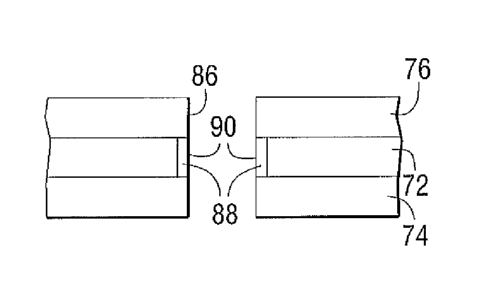
[0100] FIG. 11 is a plan view of another substrate 70 including an opening
82 passing
through the substrate. FIG. 12 is a cross-sectional view of the substrate of
FIG. 11, taken
along line 12-12. The substrate 70 includes an electrically conductive core 72
and first and
second layers of electrically insulating dielectric material 74 and 76 on
opposite major
surfaces 78 and 80 of the core. The core can have a thickness as low as about
5 um.
CA 02711649 2010-07-07
WO 2009/091460
PCT/US2008/086109
- 18 -
[01011 The
opening 82 can be created using any known technique, as described
above. The opening may have a circular cross-sectional shape with a diameter
of for
example, about 25 p.m, or another cross-sectional shape. The opening exposes
an edge 84 of
the conductive core.
[0102] To
minimize potential blocking of the vias, the core may be recessed with an
acid etch prior to application of the electrodeposited coating dielectric.
Alternatively, if the
via is blocked with unreacted electrodeposited coating, the via could be
opened with a
pressurized water spray prior to baking or laser etching after baking.
[0103] In this
example, a portion of the edge 84 of the core is removed to create a
recess having a depth Dl. The portion can be removed by etching the exposed
edge of the
core. The
etching can be accomplished, using an acid etchant for example, an
FICl/CuClx/H202 mix (where x =1,2) at a pH of about 1.5. The exact composition
of each
component will vary depending on whether the solution is fresh or at an
adjusted
equilibrium. The amount of etching has been shown to be proportional to the
speed at which
the substrate passes through the solution. Thus if the substrate passes
through the etch
solution, for example on a conveyor, the amount of etching is tunable by
changing the speed
of the conveyor. Different etchants can be used for different substrate core
materials.
[0104]
Following the etching, the edge of the core is recessed a distance D1 from the
wall 86 of the opening. Then a layer of dielectric material can be formed on
the edge of the
core using any of the previously described processes and materials. In one
example, the ratio
of the thickness of the core to the etch distance D1 is about 2.
[0105] FIG. 13
is a plan view of the substrate 70. FIG, 14 is a cross-sectional view of
the substrate of FIG. 13, taken along line 14-14. The dielectric coating 88
can be applied to
the exposed edge using electrodeposition. The surface 90 of the dielectric
layer can be
aligned with the wall 86 of the opening as shown in FIG. 14. To achieve
conformance of the
surface of the dielectric layer and the wall, the opening can be reamed or
otherwise processed
using techniques similar to those used to make the opening. For example, the
opening could
be drilled a second time, or the opening could be further shaped using a
plasma etch or other
material removal technique. In other examples, the surface of the dielectric
layer can be
recessed with respect to the wall 86, or it can protrude into the opening.
[0106] FIG. 15
is a plan view of a circuitized substrate. FIG. 16 is a cross-sectional
view of the substrate of FIG. 15, taken along line 16-16. In the example of
FIGs. 15 and 16,
a circuit 100 including conductor sections 102, 104, 106 and 108 is formed on
the substrate.
CA 02711649 2013-03-11
=
- 19 -
Conductor 104 tills the opening and is insulated from the core layer by the
electrodeposited
material 88.
[0107] In another example, one or more electrical conductors can be
formed on the
walls of the opening, as shown in FIGs. 9 and 10. Such conductors would be
electrically
insulated from the core layer by the electrodeposited dielectric material.
[0108] FIG. 17 is a plan view of a multi-layer substrate 120. FIG. 18
is a cross-
sectional view of the substrate of FIG. 17, taken along line 18-18. The
substrate includes first
and second conductive cores 122 and 124, and first, second and third layers of
insulating
material 126, 128 and 130. An opening 132 is formed in the substrate using the
techniques
described above. In this example, both cores are recessed from a wall 136 of
the opening. A
dielectric coating 138 can be selectively electrodeposited on one of the cores
122 by applying
voltage to only that core as illustrated by voltage source 140. This example
illustrates the use
of multiple cores, where only selected ones of the cores include an
electrodeposited coating
on the edge adjacent to the opening. Following electrodeposition of the
dielectric coating, the
opening could be reamed to align the surface of the dielectric coating with
the wall of the
opening. In another example, the edges of the cores may be unetched, such that
they are
aligned with the wall of the opening.
[0109] FIG. 19 is a plan view of a circuitized substrate 120. FIG. 20
is a cross-
sectional view of the substrate of FIG. 19, taken along line 20-20. FIGs. 19
and 20, a circuit
150 including conductor sections 152, 154, 156 and 158 is formed on the
substrate.
Conductor 154 is positioned in the opening and insulated from the core 122
layer by the
electrodeposited material 138. The conductor section 154 makes electrical
contact with the
core 124 at edge 160. The structure of FIGs. 19 and 20 shows that the
substrate can include
multiple cores and the edges of the cores can be selectively coated with the
dielectric coating,
thereby allowing electrical contact between a conductor in the via and the
edges of the cores
which have not been coated.
[01101 FIGs. 21 and 22 are cross-sectional views of other substrates in
accordance
with aspects of the invention. In FIG. 21 a circuit 170 including conductor
sections 172, 174
and 176 is formed on the substrate. Conductor section 174 is positioned along
the wall of the
opening and insulated from the core 122 layer by the electrodeposited material
138. The
conductor section 174 makes electrical contact with the core 124 at edge 160.
[0111] In FIG. 22 a circuit 180 including conductor sections 182, 184
and 186 is
formed on the substrate. Conductor section 184 is positioned along the wall of
the opening
and insulated from the core 122 layer by the electrodeposited material 138.
The conductor
CA 02711649 2010-07-07
WO 2009/091460
PCT/US2008/086109
- 20 -
section 184 makes electrical contact with the conductive layer 188 at edge
190. FIG. 22 is
similar to the structure of FIG. 23, but the second conductive core has been
replaced by a
conducive layer 188 and the top insulating layer has been removed.
[0112] FIG, 23 is a plan view of another circuitized substrate. FIG. 24 is
a cross-
sectional view of the substrate of FIG. 23, taken along line 24-24. In the
example of FIGs. 23
and 24, a circuit 200 including conductor sections 202, 204, 206 and 208 is
formed on the
substrate. Conductor section 204 is positioned along the sides of the opening
and is insulated
from the core layer by the electrocleposited material 88.
[0113] In another example, the dielectric coating can be removed in one or
more
predetermined locations to expose one or more sections of the edge of the
core. The
dielectric coating can be removed by a variety of methods, for example by
ablation
techniques. Such ablation typically is performed using a laser or by other
conventional
techniques, for example, mechanical drilling and chemical or plasma etching
techniques.
101141 In another aspect, the invention is directed to a process for
fabricating a
substrate assembly comprising: providing a substrate (such as any of those
described in
detail above) including a conductive core and first and second insulating
layers on opposite
sides of the core, forming an opening in the substrate to expose an edge of
the conductive
core, and electrodepositing a dielectric coating (such as any of those
described in detail
above) onto the exposed edge of the core.
[0115] The process can further include the step of removing a portion of
the
conductive core adjacent to the edge prior to applying the dielectric coating.
The dielectric
coating can be recessed from a wall of the opening, aligned with the wall, or
protruding from
the wall. To align the surface of the dielectric coating with the wall, the
opening can be
reamed.
[0116] In various aspects, the invention allows the use of current
processing
techniques for much of the substrate fabrication, while providing a method
that allows for
small via sizes. In one aspect, the invention can include a method for
preventing blocking of
the vias with the electrodeposited coating (especially with small diameter
vias) or the
removal of extraneous coating. Besides the advantage of obtaining metal core
technology
using proven laminating processes, smaller diameter (<100 microns), more
tightly packed
vias could potentially be produced. This benefit can be obtained with minimal
changes in
current production process.
[0117] It should be understood that any of the processes of the present
invention can
include one or more additional steps without departing from the scope of the
invention.
CA 02711649 2013-03-11
- 21 -
Likewise, the order in which the steps are performed may be changed as
necessary, without
departing from the scope of the invention.
101181 As used in this description, unless indicated to the contrary, the
numerical
parameters are approximations that may vary depending upon the desired
properties sought to
be obtained by the present invention. Thus each numerical parameter should at
least be
construed in light of the number of reported significant digits and by
applying ordinary
rounding techniques, or by taking typically manufacturing tolerances into
account.
[0119] Other than in the operating examples, or where otherwise
indicated, all
numbers expressing dimensions, quantities of ingredients, processing
parameters and so forth
used in the specification and claims are to be understood as being modified in
all instances by
the term "about." Accordingly, unless indicated to the contrary, the numerical
parameters set
forth in the following specification and attached claims are approximations
that may vary
depending upon the desired properties sought to be obtained by the present
invention. At the
very least, and not as an attempt to limit the application of the doctrine of
equivalents to the
scope of the claims, each numerical parameter should at least be construed in
light of the
number of reported significant digits and by applying ordinary rounding
techniques.
[0120] Notwithstanding that the numerical ranges and parameters setting
forth the
broad scope of the invention are approximations, the numerical values set
forth in the specific
examples are reported as precisely as possible. Any numerical values, however,
inherently
contain certain errors necessarily resulting from the standard deviation found
in their
respective testing measurements.
[0121] Also, it should be understood that any numerical range recited
herein is
intended to include all sub-ranges subsumed therein. For example, a range of
"1 to 10" is
intended to include all sub-ranges between and including the recited minimum
value of 1 and
the recited maximum value of 10, that is, having a minimum value equal to or
greater than 1
and a maximum value equal to or less than 10.
[01221 It will be appreciated by those skilled in the art that changes
could be made to
the embodiments described above without departing from the broad inventive
concept
thereof. It is understood, therefore, that this invention is not limited to
the particular
embodiments disclosed. The scope of the claims should not be limited by the
embodiments
set out herein but should be given the broadest interpretation consistent with
the description
as a whole.