Note: Descriptions are shown in the official language in which they were submitted.
CA 02711956 2010-07-12
WO 2009/091926 PCT/US2009/031155
INTEGRATED MAGNETIC FIELD GENERATION
AND DETECTION PLATFORM
CROSS-REFERENCE TO RELATED APPLICATIONS
[0001] This application claims priority from U.S. provisional application
serial number 61/021,861 filed on January 17, 2008, incorporated herein by
reference in its entirety.
STATEMENT REGARDING FEDERALLY SPONSORED RESEARCH
OR DEVELOPMENT
[0002] Not Applicable
INCORPORATION-BY-REFERENCE OF MATERIAL
SUBMITTED ON A COMPACT DISC
[0003] Not Applicable
BACKGROUND OF THE INVENTION
1. Field of the Invention
[0004] This invention pertains generally to detecting the presence of target
analytes, and more particularly to an integrated magnetic field generation
and detection platform.
2. Description of Related Art
[0005] As baby-boomers in developed nations retire and as the ranks of
new healthcare recipients in developing nations swell, new medical
systems are needed to weather the storm of rising healthcare costs. In
particular, Point-of-Care (POC) technologies have the potential to keep
costs at bay by enabling affordable preventative diagnostics and personal
chronic disease monitoring. Many of these POC technologies use detection
schemes that rely on the specific marking of target analyte with labels, such
as catalytic enzymes, optical markers or magnetic beads. The latter are
very useful as labels for bio-assay applications because (a) cells exhibit few
if any magnetic properties, b) signals from magnetic beads are stable with
time, (c) magnetic detection functions regardless of the opacity of the
CA 02711956 2010-07-12
WO 2009/091926 PCT/US2009/031155
sample, and (d) magnetic labeling provides added functionality such as
magnetic filtration and manipulation.
BRIEF SUMMARY OF THE INVENTION
[0006] The present invention, according to one aspect, comprises an
integrated magnetic field generation and detection platform. The platform is
capable of manipulating and detecting individual magnetic particles, such
as spherical super-paramagnetic beads, and providing biosensing
functionality. Another aspect of the invention is an integrated circuit
having,
in one beneficial embodiment, means for generating a magnetic separation
field, means for generating a magnetic concentration/magnetization field,
and means for detecting a magnetic field. In one exemplary mode of use,
magnetic beads are first manipulated using the separation field generating
means and/or the concentration/magnetization field generating means, then
magnetized using the concentration/magnetization field generating means,
and then detected using the field detecting means.
[0007] In another embodiment, an integrated circuit apparatus comprises a
substrate having an exposed surface; field detecting means embedded in
the substrate beneath the substrate surface; and
concentration/magnetization field generating means embedded in the
substrate and positioned between the field detecting means and the
substrate surface.
[0008] In another embodiment, an integrated circuit apparatus comprises a
substrate having a trench with an exposed surface, the trench having a
sidewall with an upper ridge portion; field detecting means embedded in the
substrate beneath the substrate surface; concentration/magnetization field
generating means embedded in the substrate and positioned between the
field detecting means and the substrate surface; and separation field
generating means in the upper ridge portion of the sidewall.
[0009] In another embodiment, an integrated circuit apparatus comprises a
substrate having a plurality of trenches, each trench having an exposed
surface area and a sidewall with an upper ridge portion; field detecting
means embedded in the substrate beneath the substrate surface; and
concentration/magnetization field generating means embedded in the
-2-
CA 02711956 2010-07-12
WO 2009/091926 PCT/US2009/031155
substrate and positioned between the field detecting means and the
substrate surface.
[0010] In another embodiment, the integrated circuit is a component of a
biosensor device. In one exemplary mode of use, at least a portion of the
surface of the integrated circuit is functionalized by coating it with a
biochemical agent that binds tightly (i.e., specifically) with a target
analyte.
The magnetic beads are similarly coated or conjugated with one or more
biochemical agents that that bind specifically with the target analyte. The
sample is introduced and the target analyte binds to the functionalized
surface of the integrated circuit. The magnetic beads are introduced and
they either bind specifically to the surface of the trench via the biochemical
complex involving the target antigen, or non-specifically. The magnetic
beads may bind to the analyte first, before they settle to the surface of the
substrate, at which point the analyte also binds to the substrate, thereby
tethering the bead to the surface. The non-specifically bound beads can
then be removed by on-chip magnetic washing forces, and the remaining
specifically bound beads can be detected by magnetic field detecting
means integrated beneath the surface of the substrate. This biosensor can
therefore be used to determine the concentration of infectious disease
agents in blood or serum.
[0011] In various embodiments, the concentration/magnetization field
generating means can comprise a plurality of micro-coils, a current line
(e.g., conductor), or other elements that generate a magnetic field,
positioned between the surface of the substrate and the field detecting
means.
[0012] In one embodiment, the concentration/magnetization field generating
means comprises a plurality of individual magnetic field generating
elements, and the field detecting means comprises a plurality of individual
magnetic field detecting elements, wherein each magnetic field generating
element is paired with a magnetic field detecting element to create a
stacked unit cell.
[0013] In various embodiments, the field detecting means can comprise a
plurality of Hall sensors, variable inductance wires, or other elements that
-3-
CA 02711956 2010-07-12
WO 2009/091926 PCT/US2009/031155
can sense a magnetized object.
[0014] In various embodiments, the separation field generating means can
be placed laterally apart from the concentration/magnetization field
generating means either in the same plane or in a plane above the
concentration/magnetization field generating means.
[0015] In various embodiments, the separation field generating means can
comprise current lines (e.g., conductors) or other elements that generate a
magnetic field.
[0016] In various embodiments, at least a portion of the exposed surface
area of the substrate is functionalized with a biochemical agent that binds
with a target analyte.
[0017] In various embodiments, at least a portion of the unit cells are
addressable.
[0018] Further aspects of the invention will be brought out in the following
portions of the specification, wherein the detailed description is for the
purpose of fully disclosing preferred embodiments of the invention without
placing limitations thereon.
BRIEF DESCRIPTION OF THE SEVERAL
VIEWS OF THE DRAWING(S)
[0019] The invention will be more fully understood by reference to the
following drawings which are for illustrative purposes only:
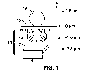
[0020] FIG. 1 schematically shows an integrated micro-coil/Hall sensor pair
according to an embodiment of the invention with a magnetic bead
positioned above the Hall sensor/micro-coil pair for context.
[0021] FIG. 2 is a schematic plan view of two micro-coil/Hall sensor
elements of the type shown in FIG. 1, implemented in a loose array.
[0022] FIG. 3 is a schematic diagram of a micro-coil/Hall sensor pair from
an active sensor array and a "dummy" micro-coil/Hall sensor pair from a
reference array, both connected to an on-chip amplifier (OCA) and analog
to digital converter (ADC) and digital signal processor (DSP), for rejection
of
common-mode applied fields from the coils to be rejected while the
differential induced field from the bead is amplified.
-4-
CA 02711956 2010-07-12
WO 2009/091926 PCT/US2009/031155
[0023] FIG. 4 is the spectrum of the output of the ADC of FIG. 3 measured
with a 1 Hz noise bandwidth, directly after auto-zeroing (upper graph) and
after application of the bead (lower graph).
[0024] FIG. 5 is a perspective view of an array of integrated adjacent micro-
coil/Hall sensor elements positioned in a row along the bottom of an etched
trench with current lines along its ridges for integrated magnetic separation
of magnetic beads, and showing a plurality of beads positioned above the
micro-coil/Hall sensor elements for context.
[0025] FIG. 6A through FIG. 6E is a cross-sectional flow diagram showing
an embodiment of a reactive ion etching process used in fabrication of the
integrated circuit shown in FIG. 5.
[0026] FIG. 7 is a partial cross-sectional schematic view of the array shown
in FIG. 5, taken through the center of a micro-coil/Hall sensor pair,
illustrating the motion on a bead imparted by the magnetic force from the
current line on the upper ridge of the trench, where the bead is moved away
from the micro-coil/Hall sensor pair.
[0027] FIG. 8 is a schematic partial plan view of the array shown in FIG. 5,
showing a specifically bound (e.g., biologically bound) bead and a non-
specifically bound bead positioned above a micro-coil/Hall sensor pair.
[0028] FIG. 9 is a schematic partial plan view of the array shown in FIG. 5,
showing the non-specifically bound bead in FIG. 8 being removed due to
the magnetic force imparted on the bead by a current line either embedded
in the substrate or running along the upper ridge of the trench, and showing
the specifically bound bead remaining in place.
[0029] FIG. 10 is an example of a force-distance curve corresponding to the
array shown in FIG. 9.
[0030] FIG. 11 is a partial cross-sectional schematic view of the array
shown in FIG. 5, illustrating the motion on a bead imparted by the magnetic
force from a micro-coil, where the bead is moved into position over the Hall
sensor /micro-coil pair.
[0031] FIG. 12 is a partial cross-sectional schematic view of a "trenchless"
embodiment of a sensor array according to the present invention,
illustrating the motion on a bead imparted by the magnetic force from the
-5-
CA 02711956 2010-07-12
WO 2009/091926 PCT/US2009/031155
separation current line embedded in the substrate, where the bead is
moved away from a concentration/magnetization current line.
[0032] FIG. 13 is a series of micrograph plan views showing magnetic
beads being pulled to the sensor area over time.
[0033] FIG. 14 is a schematic partial plan view of the array shown in FIG.
12, showing a specifically bound (e.g., biologically bound) bead and a non-
specifically bound bead positioned above Hall sensors.
[0034] FIG. 15 is a schematic partial plan view of the array shown in FIG.
12, showing the non-specifically bound bead in FIG. 14 being removed due
to the magnetic force imparted on the bead by a current line either
embedded in the substrate and showing the specifically bound bead
remaining in place.
[0035] FIG. 16A through FIG. 16E is a cross-sectional flow diagram
showing an embodiment of a reactive ion etching process used in
fabrication of the integrated circuit shown in FIG. 12.
[0036] FIG. 17 is a bottom plan view of a printed circuit board configured for
supporting an integrated circuit according to the present invention for
biological sensing, with the integrated circuit shown exploded away from
the circuit board.
[0037] FIG. 18 is a top plan view of an embodiment of the integrated circuit
shown in FIG. 17.
[0038] FIG. 19 is a partial cross-sectional schematic view of the circuit
board shown in FIG. 17 with an attached integrated circuit shown in FIG.
18, and illustrating a seal ring to prevent leakage of a biological fluid.
[0039] FIG. 20 illustrates an integrated circuit as shown in FIG. 18 with the
sensor area having four trenches of varying width.
[0040] FIG. 21 A and 21 B are micrographs showing negative and positive
control of purified human IgG assay, respectively.
[0041] FIG. 22A and 22B are graphs showing on-chip assay results and
washing efficiency, respectively.
[0042] FIG. 23 is an electrical circuit diagram of a bank of eight micro-
coil/Hall sensor elements according to an embodiment of the invention.
[0043] FIG. 24 is an electrical circuit diagram of sixteen banks of the micro-
-6-
CA 02711956 2010-07-12
WO 2009/091926 PCT/US2009/031155
coil/Hall sensor elements shown in FIG. 23, with addressing schemes
shown on the left.
[0044] FIG. 25 schematically shows the sixteen banks of micro-coil/Hall
sensor elements of FIG. 24 with current lines for generating the magnetic
separation forces being placed adjacent to the banks of Hall sensors, and
with the dashed lines showing the areas of micro-coil/sensor element
banks.
DETAILED DESCRIPTION OF EMBODIMENTS
OF THE INVENTION
[0045] Referring first to FIG. 1 and FIG. 2, magnetic bead detection
according to the present invention is based on embedding, beneath an
exposed surface area of a substrate, (i) means for detecting a magnetic
field, and (ii) means for generating a magnetic concentration/magnetization
field between the field detecting means and the substrate surface. In the
embodiment shown, the field detecting means and
concentration/magnetization field generating means form a unit cell 10,
which in this embodiment comprises a Hall sensor 12 stacked beneath a
micro-coil 14. The micro-coil and Hall sensor, respectively, polarize and
detect an individual super-paramagnetic bead 16 at the surface 18 of a
CMOS integrated circuit (IC) 20 into which the micro-coil/Hall sensor pair
are integrated. In one embodiment, the micro-coils are single turn current
loops having an inner radius a and line width w, and the Hall sensors are n-
well square planar sensors having side dimensions d and thickness t.
Each micro-coil and Hall sensor in a unit cell is preferably positioned
coaxially along the z-axis as illustrated, with the micro-coil stacked above
the Hall sensor and positioned closest to the surface of the integrated
circuit.
[0046] In this regard, the z-component of the micro-coil's applied magnetic
field can be described by the off-axis field of a current loop as follows:
(Z) _ Poicoil
'applied
2TC (a+ry +z2
-7-
CA 02711956 2010-07-12
WO 2009/091926 PCT/US2009/031155
z_r2 _ z
a E(k) (a + r)z + zz ? Oar + K(k)
(1)
where Po is the permeability of free space, Ieo11 is the current through the
coil, r is the distance from the center of the coil to the point of
observation,
E(k) and K(k) are the complete elliptical integral functions of the 1st and
2nd
kind and k is given by:
4ra
k (a+r)z +zz (2)
[0047] According to equations (1) and (2), 10mA of current through the
micro-coil will produce a magnetic field Bapplied(zbead)=800pT at the center
of
the bead and an average field BapplZed(zHa1)=750uT across the Hall sensor
contacts.
[0048] The induced magnetization field of the bead, Bbead, is approximated
by equation (3) below:
B = ,uo 3(r . mbead)r - (r . r)mbead (3)
bead 4,r rs
where r is the vector from the point of observation to the center of the
bead. saa is the bead's magnetic moment, given by
mbead = XbVbBapplied (zbead )z , where Xb and Vb are the bead's magnetic
susceptibility and volume. As can be seen from equation (3), the bead's
induced magnetization field decays with the cube of the distance r, so the
dielectric layer above the micro-coil/Hall sensor pair is etched back using
conventional techniques. For Bapplied(zbead)=800pT, equation (3) estimates
the z-component of the average induced magnetization field to be
Bbead,z=10.2pT across the contacts of the Hall sensor.
[0049] The equation for the Hall sensor voltage as a function of the z-
component of the magnetic field is given by:
VH = GH po W1111 Bz
LHall (4)
where WHa11 and LHa11 are the width and length of the Hall plate, in this case
both equal to d, and where GH is the Hall effect geometric factor. The
calculated Hall sensitivity of 34V/AT is in line with measurement results for
-8-
CA 02711956 2010-07-12
WO 2009/091926 PCT/US2009/031155
uniform fields, but a decreased sensitivity was noted for the highly non-
uniform field from the coil.
[0050] For a more accurate value of the expected applied field from the coil
and the magnetization field from the bead, the conditions shown in FIG. 1
were simulated using the research edition of MagNet by Infolytica. Table 1
gives the calculated, simulated and measured z-component of the applied
coil field and bead magnetization field, observed from the plane of the Hall
sensor. As seen in Table 1, the measured applied field from the coil is 50x
larger than the induced field from the bead. To mitigate this undesirable
dynamic range constraint, a differential architecture was employed, which
subtracts the signal of a reference Hall sensor with no bead from the signal
of a Hall sensor with a bead. This configuration is illustrated in FIG. 3,
which is a schematic diagram of a micro-coil/Hall sensor pair 10a from a
sensor array and a "dummy" or "reference" micro-coil/Hall sensor pair 10b
from a reference array, both of which are connected to an on-chip amplifier
(OCA) 100 and an off-chip 16-Bit analog to digital converter (ADC) 102
followed by digital signal processor (DSP) 104.
[0051] The configuration in FIG. 3 allows the common-mode applied fields
from the coils to be rejected while the differential induced field from the
bead, detected by the Hall sensor in pair 1 Oa, is amplified. For further
attenuation of the common-mode applied fields, a calibration feedback loop
sets the current through micro-coil in pair 1 Ob such that the output of the
OCA 100 is zeroed out. The feedback loop applies an additional current in
the reference coil to cancel out any residual field signal due to mismatch.
The entire detection system noise is dominated by the 1/f noise of the OCA
100 with a spot noise of 300nTNHz at the detection frequency of 50kHz.
After amplification, the output is digitized by the off-chip ADC 102 and
processed by DSP 104.
[0052] In one embodiment, before the beads are applied, the system
calibrates itself by auto-zeroing the output of the OCA 100 with the
fundamental, f,, of a 1 OmA, 50kHz square current wave through the micro-
coils. In a manufacturing paradigm, this internal self calibration could be
performed on the factory floor since the system does not suffer from
-9-
CA 02711956 2010-07-12
WO 2009/091926 PCT/US2009/031155
appreciable drift. Alternatively, this self calibration can be performed
immediately before patient use. Once the system has been calibrated, it is
ready for detection. In our experiments, the beads were desiccated on the
surface of the IC and then were individually micro-manipulated over the Hall
sensors. The same square current wave that was used for calibration is
sent through the coils and the new value of the fundamental at f, is
recorded.
[0053] FIG. 4, which presents measurements from the Hall sensors directly
after calibration and after a bead has been applied, shows that this system
is capable of detecting individual magnetic beads with 33dB of SNR for a
1 Hz noise bandwidth (i.e. for an integration time = 1 s). FIG. 4 is the
spectrum of the output of the ADC directly after auto-zeroing (upper graph)
and after application of the bead (lower graph).
[0054] Referring now to FIG. 5 and FIG. 6, an example of the fabrication of
an embodiment of an IC 20 is illustrated. FIG. 5 shows a single row of
interconnected micro-coil/Hall sensor unit cells 10 embedded beneath the
bottom surface 18 of an etched trench 22, and separation field generating
means in the form of current lines (electrical conductors) 24a, 24b
embedded along the upper ridge portions of sidewalls 26a, 26b. Each
micro-coil and Hall sensor in a unit cell is preferably positioned coaxially
along the z-axis as illustrated, with the micro-coil vertically stacked above
the Hall sensor and positioned closest to the exposed surface 18 of the
trench 22. FIG. 5 also shows a plurality of beads 16 positioned above the
micro-coil/Hall sensor elements for context. FIG. 6A is a cross-sectional
view of IC 20 after conventional CMOS fabrication on an Si/Si02 substrate,
but prior to the post-processing which creates trench 22. In this
embodiment, the Hall sensors 12 are embedded in the Si layer 28 and the
micro-coils 14 are embedded in the Si02 layer 30.
[0055] To reduce distance from the Hall sensors to the beads, we used a
directional plasma etch to remove most of the Si02 30 from above the
micro-coil/Hall sensor area. This creates the trench 22 in the CMOS
substrate. The top of the trench is determined by a protective top metal
layer 32 and corresponds to the original surface of the IC (FIG. 6A) minus
-10-
CA 02711956 2010-07-12
WO 2009/091926 PCT/US2009/031155
the dielectric etched during post processing described below with reference
to FIG. 6B through FIG. 6E. The bottom of the trench is determined by a
metal etch stop layer 34 placed directly above the metal micro-coils 14.
The metal current lines 24 are integrated along the upper ridge portions of
sidewalls 26a, 26b of the trenches at a location where magnetic forces
generated when current runs through the current lines will be sufficient to
manipulate and pull magnetic beads away from the sensor area and toward
the sides of the trench. In this embodiment, the current lines 30 are
positioned approximately 2.5pm above the bottom of the trench to
accommodate approximately 2.8pm diameter beads. The sidewalls of the
trench begin at approximately 15pm from the outer edge of the micro-coils;
thus, the trench width is approximately 34.2pm in this example.
[0056] Post-processing of the IC shown in FIG. 6A generally proceeds as
illustrated in FIG. 6B through FIG. 6E. In FIG. 6B, photoresist 42 is spun on
and patterned to expose the sensor area. The connection pads and all
other circuitry are protected by the photoresist. FIG. 6C shows Si02
reactive ion etching (RIE). Here, the photoresist 36, top metal 32 placed
above the current lines 24, and metal 34 placed above the micro-coils 14
are used as the etch stop to the RIE. In FIG. 6D, an aluminum etch is used
to remove the etch stop metal layer 34. The metal 32 that remains after the
aluminum etch can safely remain since it is not electrically connected to IC
and served only to define the trench and protect the current lines from
washing. Finally, in FIG. 6E, a chromium seed layer and gold substrate
layer 38 is evaporated through a hard mask (e.g., shadow mask) 40. This
hard mask 40 allows the chromium and gold to settle only on the sensor
area. In this embodiment, the photoresist is removed before the gold is
evaporated onto the CMOS IC through a shadow mask 40. In another
embodiment, the photoresist can be used as a lift-off mask for gold
deposition to omit the shadow mask altogether. Trenching is now complete
and the IC 20 is ready to be functionalized.
[0057] Referring again to FIG. 3 and the related discussion, a reference
sensor array would be processed in a similar manner, except that the
dielectric in the reference array would not be etched back to create a
-11-
CA 02711956 2010-07-12
WO 2009/091926 PCT/US2009/031155
trench. Therefore, the sensors would never have a bead above them.
[0058] Example
[0059] To test the above-described configuration, we embedded micro-coils
approximately 1.Opm below the bottom of the trench in the lowest CMOS
metallization layer, and we embedded Hall sensors approximately 2.8pm
below the micro-coils. The micro-coils that we used were single turn
current loops having an inner radius a=1.7pm, a line width w=0.5pm, and
an outer diameter of 4.2pm. The Hall sensors that we used were n-well
square planar sensors having side dimensions d=4.7pm and thickness
t=1 pm. For optimal performance, power consumption and packing density,
our calculations showed that the overall sizes of the micro-coils, the Hall
sensors and the beads should all be approximately the same, and in this
experiment were 4pm. We found that the micro-coils were capable of
generating fields of up to 800pT for 10mA of current, and that the Hall
sensors exhibited a sensitivity of 34V/AT for a 2mA bias current. Using a
differential amplifier, single spherical magnetic beads having a diameter of
approximately 2.8pm, were detected with 33dB of SNR for a 1 Hz noise
bandwidth.
[0060] In the embodiments described above, the
concentration/magnetization field generating means comprises a plurality of
individual magnetic field generating elements (e.g., micro-coils), and the
field detecting means comprises a plurality of individual magnetic field
detecting elements (e.g., Hall sensors), wherein each micro-coil is paired
with a Hall sensor to create a stacked unit cell. It will be appreciated,
however, that the configuration of the invention is not limited to that which
is
described above. For example, the concentration/magnetization field
generating means can comprise a current line (e.g., conductor) or other
element that generates a magnetic field, positioned between the surface of
the substrate and the field detecting means. Furthermore, the field
detecting means can comprise a variable inductance wire or other element
that can sense a magnetized object. Also, not only can the separation field
generating means be implemented in the form of a current line placed in the
upper ridge of a trench sidewall as previously described, but alternatively,
-12-
CA 02711956 2010-07-12
WO 2009/091926 PCT/US2009/031155
the separation field generating means can be placed laterally apart from the
concentration/magnetization field generating means in the same plane
rather than in a plane above the concentration/magnetization field
generating means. The separation field generating means can also be
used to magnetize the magnetic beads at an arbitrary frequency which
obviates the need for the concentration/magnetization field generating
means. The current through the separation field generating means can be
changed arbitrarily as well.
[0061] Integrated circuits according to the present invention are particularly
well suited for biosensing applications. For such applications, the
integrated circuit and magnetic beads can be adapted to specifically (e.g.,
biologically) bind to target analytes. For example, the trench surface of the
integrated circuit would be coated with one or more biochemical agents that
binds tightly (i.e., specifically) with the target analyte. The magnetic beads
would similarly be coated or conjugated with one or more biochemical
agents that that bind specifically with the target analyte. For testing, we
have employed mono-dispersed M280 Dynal beads of 2.8pm in diameter
that were functionalized with a streptadivin coating. These particular beads
have been well characterized and are known to be effective as reporting
agents.
[0062] When the sample is introduced into the sensor area, the target
analyte binds to the surface of the integrated circuit. When the magnetic
beads are introduced, they will either bind specifically to the functionalized
surface of the substrate via the biochemical complex involving the target
antigen, or non-specifically. The non-specifically bound beads can then be
removed by on-chip magnetic washing forces, and the remaining
specifically bound beads can be detected by the magnetic sensors
integrated beneath the surface of the trench. In general, it is possible to
detect immobilized magnetic particles including non-specifically bound
beads.
[0063] Referring also to FIG. 7 through FIG. 10, the current lines 24 are
placed above the plane of the beads to eliminate the component of the
force that pull the beads down into the plane of the IC, thus improving the
-13-
CA 02711956 2010-07-12
WO 2009/091926 PCT/US2009/031155
magnetic separation efficiency. In the embodiment shown, the current
lines are placed approximately 2.5pm above the surface 18 of the
substrate. FIG. 7 illustrates the leftmost current line being turned on while
the rightmost current line is turned off. The double X's in the leftmost
current line 24a denote the current flow into the paper; the rightmost current
line 24b is not energized. The magnetic field 42 generated by the leftmost
current line creates a magnetic force 44 which imparts motion to the bead
and causes the bead to be moved away from the micro-coil/Hall sensor pair
and toward the side of the trench. Optionally, the current can be alternated
between the left current line 24a and the right current line 24b by arbitrary
digital modulation. FIG. 8 is a schematic partial plan view of the array
shown in FIG. 5, illustrating a specifically bound bead 16a and a non-
specifically bound bead 16b positioned above a micro-coil/Hall sensor pair
1 Oa, 1 Ob, respectively, and in relation to a current line 24. FIG. 9 is a
schematic partial plan view of the array shown in FIG. 5, showing the non-
specifically bound bead 16b in FIG. 8 being removed due to the magnetic
force 44 imparted on the bead by the current line 24 in the upper ridge
portion of the trench sidewall and the specifically bound 16a bead
remaining in place. FIG. 10 is an example of a force-distance curve
corresponding to the array shown in FIG. 9.
[0064] Note that if the magnetic beads settle too far from the sensors they
will not be detected. Accordingly, in the preferred embodiment, current
carrying conductors are placed in the substrate, for example in the same
plane as the micro-coils. Even more preferably, the micro-coils 14 are used
as these current carrying conductors as illustrated in FIG. 11. In FIG. 11,
the X and circle-dot in the micro-coil 14 indicate current flow in the micro-
coil into the paper and out of the paper, respectively. A magnetic field 46 is
generated by the micro-coil 14, and motion on the bead 16 is imparted by
the magnetic force 48 which results in bead being moved into position over
the micro-coil/Hall sensor element. Here, the current lines in the upper
ridge portions of the trench sidewalls are not energized but, instead, current
passing through the micro-coils generates magnetic forces that pull the
magnetic beads settling out of solution directly over the sensor area.
-14-
CA 02711956 2010-07-12
WO 2009/091926 PCT/US2009/031155
[0065] FIG. 12 through FIG. 16 illustrate that the invention can be embodied
in various other ways. For example, FIG. 12 illustrates an essentially
"trenchless" embodiment, since there are no sidewalls within which to place
the separation field generating means. Accordingly, instead of being
placed in the upper ridge portion of a trench sidewall, the separation field
generating means, current line 24, is shown embedded beneath the surface
of the substrate in the same plane as concentration/magnetization field
generating means. In addition, FIG. 12 shows that, instead of being a
plurality of micro-coils, the concentration/magnetization field generating
means can be a current line 50 placed above the field detecting means 12
and running along the length of the substrate. These configurations,
however, are functionally equivalent to the previously-described
embodiments.
[0066] For example, current line 50 will generate a
concentration/magnetization field as described above. FIG. 13 is a series
of micrograph plan views showing the magnetic beads being pulled to the
sensor area over time. As can be seen, the magnetic beads concentrate
directly above the sensor area as current is passed through the current line
50. The current generates magnetic forces that pull the beads settling out
of solution to the sensor area. To produce the effect shown in FIG. 13, we
passed 3mA of current through the current line (centermost dashed line) so
as to pull the magnetic beads that are settling to the surface over the
sensor area bounded by the outer dashed lines. The same effect would
result from energizing micro-coils as previously described.
[0067] Furthermore, current line 24 will remove non-specifically bound
beads as described above. For example, FIG. 14 illustrates a specifically
bound bead 16a and a non-specifically bound bead 16b positioned above
Hall sensors 12a, 12b, respectively, and in relation to the current line 50.
FIG. 15 illustrates the non-specifically bound bead 16b in FIG. 14 being
removed due to the magnetic force 44 imparted on the bead by the current
line 24.
[0068] As indicated above, FIG. 12 illustrates an essentially "trenchless"
embodiment, since there are no sidewalls within which to place the
-15-
CA 02711956 2010-07-12
WO 2009/091926 PCT/US2009/031155
separation field generating means. In this regard, by "trenchless" we
means that the individual rows of sensors in a multiple row IC are not
separated by sidewalls. This is illustrated in FIG. 16 which shows an
example fabrication process for an IC with two sensor rows. The
processing would follow steps similar to those described in relation to FIG.
6. Those of ordinary skill in the art will readily understand the details of
the
process shown in FIG. 16 from the discussion of FIG. 6 and description of
the IC above.
[0069] For the foregoing discussion, it should be appreciated that the
combination of magnetic separation field generating means such (e.g.,
current lines) and the magnetic concentration/magnetization field
generating means (e.g., current lines; micro-coils) embedded in the
substrate above the sensors beneficially allows for manipulation of the
magnetic beads. Beads can be moved away from the sensors or
concentrated over the sensors by energizing either the separation field
generating means or the concentration/magnetization field generation
means.
[0070] By energizing the concentration/magnetization field generating
means, but not the separation field generating means, all of the beads can
be concentrated above the sensor area, where at least a portion of the
beads will specifically bind to the surface of the trench. In one exemplary
mode of operation, the concentration/magnetization field generating means
is then turned off and the separation field generating means is turned on to
displace (e.g., magnetically wash) the non-specifically bound beads from
above the sensors. Once the non-specifically bound beads are removed by
the magnetic forces generated by the separation field generating means,
the separation field generating means is turned off, and the
concentration/magnetization field generation means is turned on again to
magnetize the specifically bound beads that remain. The field detecting
means simultaneously detects the specifically bound beads that are
magnetized by the concentration/magnetization field generating means.
[0071] Optionally, in another exemplary mode of operation, we can leave
the separation field generating means turned on during the detection
-16-
CA 02711956 2010-07-12
WO 2009/091926 PCT/US2009/031155
process to prevent non-specifically bound beads that were previously
removed from the sensor area from being drawn back to the sensor area
due to the forces generated by the current through the
concentration/magnetization field generating means. Further, we can
optionally switch current to separation field generating means on either side
of the sensor at a variable frequency so that the non-specifically bound
beads are pulled to either side of the sensor area and not just in one
direction. The separation field generating means can be kept energized
during detection, with the current flowing through them at the same or
different frequency than the current through the
concentration/magnetization field generating means. Detection can be
performed at the same time as the washing to obtain a real time analysis of
the washing effectiveness.
[0072] Referring now to FIG. 17, for use in biosensing and other
applications, the integrated circuit 20 would necessarily employ electrical
connections to external devices. To facilitate use in such applications, the
integrated circuit would preferably be flip chip bonded to one side of a
printed circuit board (PCB) 200 as illustrated in FIG. 17. In this
embodiment, the printed circuit board has a hole 202 between both sides to
allow biological fluids pass through the hole from the other side of the
circuit
board to reach the surface of the IC.
[0073] Referring also to FIG. 18 and FIG. 19, a metal ring 204a preferably
surrounds the sensor area 206 to isolate the connection pads 208a on the
IC and corresponding connection pads 208b on the PCB from the biological
fluid 210 to which the sensor area 206 is exposed. This metal ring is
preferably solder bumped and soldered to a corresponding ring 204b on the
printed circuit board. The IC is flip-chip bonded to the bottom of the PCB in
a way that simultaneously bonds the connection pads and the solder ring
with solder bumps 212. This allows the sensor area 206 to be exposed to
the biological fluid 210 via hole 202, but keeps the biological fluid isolated
from the electrical connections 208. As can be seen, the solder seal ring
encircles the sensor area, thus inhibiting the biological fluid from short-
circuiting the electrical connections.
-17-
CA 02711956 2010-07-12
WO 2009/091926 PCT/US2009/031155
[0074] Referring again to FIG. 17, in one embodiment the PCB 200 is
configured as a removable cartridge having printed connector pads 214 at
one end for mating with a corresponding socket. Accordingly, the
aforementioned printed circuit board with a flip bonded IC on one side can,
for example, be a component of a cartridge-based blood assay system. In
one embodiment, a vial is seated into a holder on the opposite side of the
circuit board, with the circuit board end of the vial opening into the hole to
the surface of the IC. The opposite end of the vial would have a mouth with
a cap, plug or other type of sealing lid to allow fluid to be contained in the
vial. This assembly forms a cartridge that can be used for the assay. In
one embodiment, the sensor area comprises multiple arrays. FIG. 18 and
FIG. 20 illustrate the integrated circuit with a sensor area 206 that
comprises four sensor arrays 216a, 216b, 216c, and 216d of varying widths
to sense different biological components. In the example shown, the widths
of sensor arrays 216a, 216b, 216c and 216d are 10pm, 15 pm, 20 pm and
pm, respectively, and the trenches are 200pm in length.
[0075] Using the above-described cartridge, for example, the following
exemplary protocol can be followed for the assay of whole blood.
(a) When ready to run assay, the user inserts the cartridge into a
20 reader and initiates a calibration process.
(b) After calibration is complete, whole blood is taken from a finger
prick and placed onto a membrane filter at the mouth of the vial.
(c) The user then closes the lid to the vial and agitates the contents
of the vial by turning it over several times for approximately 30 seconds.
25 (d) As the solution in the vial is agitated, the target analyte diffuses
through the membrane filter into the vial.
(e) Magnetic beads in the vial, conjugated with one or more bio-
chemical agents stick specifically to the target analyte that has diffused in
the vial.
(f) The magnetic beads settle to the surface of the IC which is also
coated with one or more bio-chemical agents that binds to the analyte.
(g) The beads that settle to the surface of the IC but that are not
tethered to the surface specifically via a strong biochemical complex are
-18-
CA 02711956 2010-07-12
WO 2009/091926 PCT/US2009/031155
removed by magnetic forces generated on-chip.
(h) The remaining beads are strongly tethered to the surface of the
IC are detected by an array of integrated magnetic sensors embedded in
the substrate.
(i) The signal from the beads are processed on-chip and posted on
the reader's display.
[0076] In another embodiment, the magnetic beads would first be incubated
in a separate vial with the filtered raw sample before being introduced in the
vial containing the detection IC.
[0077] Preferably, the sample to be assayed is first prepared for separating
the species to be assayed from interfering agents. This can be carried out,
for example, using a membrane filter to block particulate matter such as
whole blood cells from physically interfering with the on-chip assay. Other
approaches include using (a) an immunochromatographic strip, (b) fluid
delivery systems such as microfluidics or patterned capillary channels, (c)
conventional centrifugation, and (d) column chromatography. Sample
preparation systems such as membrane filters and
immunochromatographic strips can be augmented by chemical
functionalization to block interfering agents, much like column
chromatography.
[0078] Example
[0079] In a functionalization experiment, we evaporated gold on the surface
of the IC and an Fc specific anti-Human IgG was physio-adsorbed on the
surface. FIG. 21A shows the negative control that ensures that specifically
bound beads remain stationary during magnetic separation; a solution of
purified Human IgG was incubated and the excess IgG was washed away.
A primary biotinylated Fab specific anti Human IgG was added. Lastly the
streptavidin coated 2.8pm beads were added and let to incubate. Here,
50mA of current was passed through the current lines generating a force of
2pN at the center of the trench. 99% of specifically bound beads remained
stationary. FIG. 21 B shows the positive control that ensures that non-
specifically bound beads are removed during magnetic separation. The
protocol is the same as the positive control, with the exception that the
-19-
CA 02711956 2010-07-12
WO 2009/091926 PCT/US2009/031155
Human IgG is never added. Results show that 99% of non-specifically
bound beads are removed. FIG. 22A and 22B are graphs showing on-chip
assay results and washing efficiency, respectively. Note that the surface
functionalization scheme described above is just an example. Gold does
not necessarily have to be deposited, and other chemical binding agents
can also be used to attach antibodies or other chemical species to the
surface.
[0080] Accordingly, this biosensor is particularly well suited for determining
the concentration of infectious disease agents in blood or serum.
[0081] It will be appreciated that the micro-coil/Hall sensor elements can be
connected in various circuit configurations. For example, FIG. 23 illustrates
a circuit 300 comprising a row of eight serially connected micro-coil/Hall
sensor elements in a single trench. While current runs through all the
micro-coils within the row at the same time, the Hall sensors are individually
addressable for detection of individual magnetic beads. In other
embodiments, multiple Hall sensors can be activated at the same time. The
signal from the Hall sensors can be read out in parallel or multiple
magnetization frequencies can be used in a frequency division multiplexing
scheme. Each Hall sensor is connected to three NMOS switches 302, one
for the power supply and two for the differential magnetic signal. When a
Hall sensor is activated, all of the switches are activated. Other
configurations are possible with additional or fewer switches. The key is
that each Hall sensor is individually addressable, and that several Hall
sensors can be addressed and activated at the same time. Also, multiple
concentration/magnetization lines or micro-coils can be activated at the
same time and multiple separation lines can be activated at the same time.
[0082] Note also that an IC with multiple banks can be configured in an
electronically addressable array so that each IC can also perform
multiplexed assays since the array is addressable and different portions of
the array can be functionalized with different bio-chemical agents. The
magnetic concentration, the magnetic separation the fine detection
resolution and high level of integration offered by this system combine for a
detection mechanism that is rapid, accurate, easy to use and inexpensive.
-20-
CA 02711956 2010-07-12
WO 2009/091926 PCT/US2009/031155
We anticipate that one hundred twenty eight micro-coil/Hall sensor
elements with parallelized reading and integrated magnetic washing of non
specific biological interactions would be combined into a fully integrated bio-
assay platform.
[0083] For example, FIG. 24 illustrates a circuit 400 with sixteen instances
(e.g., sixteen banks or rows) of the circuit 300 shown in FIG. 23 to create
an 8x1 6 array for a total of one-hundred twenty-eight micro-coil/Hall sensor
elements. The digital logic for addressing and decoding are integrated on-
chip. The signal from a Hall sensor in the sensor array is subtracted from
the signal of a dummy Hall sensor that cannot have any beads above it.
The array of dummy Hall sensors, while not shown here, is placed away
from the sensor area that is exposed to fluid. Various addressing schemes
are also shown on the left in FIG. 24. Preferably, the current lines for
generating the magnetic forces for removing the non-specifically bound
beads are placed along the ridges of the etched trenches, adjacent to the
row of eight micro-coil/Hall sensor elements, as illustrated in FIG. 25. The
dashed lines surrounding the rows of Hall micro-coil/Hall sensor elements
indicate the area of the etched out trench portions.
[0084] From the foregoing, it will be appreciated that the platform described
can be used for many applications, including, but not limited to, the
following.
[0085] 1. Diagnostics:
(a) Viral vs. bacterial infections;
(b) Parallel or multiplexed assays;
(c) DNA micro-array;
(d) Oral bacteria screenings;
(e) Glucose, cholesterol, metabolites, small molecules etc.
[0086] 2. Environmental assays:
(a) Food contamination;
(b) Water/soil contamination.
[0087] 3. Proteomics:
(a) Protein-protein binding force measurements;
(b) Protein-protein binding resonant frequencies;
-21-
CA 02711956 2010-07-12
WO 2009/091926 PCT/US2009/031155
(c) DNA methylation.
[0088] 4. Magnetic Bead AFM:
(a) No 1/f noise at low frequencies;
(b) Force and frequency digitally controlled.
[0089] 5. Magnetic Bead Characterization:
(a) Explore magnetic properties of single beads of different
sizes and with different magnetic nano-particles.
[0090] 6. Low Cost Bio-sensor Networks:
(a) Integrated transmitter can send assay results directly to
base station for statistical analysis;
(b) Real-time outbreak/contamination monitoring.
[0091] 7. Magnetic sensor Arrays:
(a) Magnetic field and magnetic gradient field quantization.
[0092] The appeal of this system can be understood by analyzing the
results in the proper context of what we consider makes a good bio-sensor:
[0093] 1. Cost - Biological contamination concerns dictate that Point-of-
Care sensor cartridges be disposable, thus putting a premium on low cost
implementations. From an overall system perspective, CMOS is the most
cost effective option since it allows the integration of the sensor front-end
with the necessary signal processing back end.
[0094] 2. Speed - The current detection time of = 1 s can be reduced by
compromising the abundant SNR. For a large array of sensors, CMOS also
has the distinct advantage of offering highly parallelized readout at low
cost.
In addition to parallel hardware, multiple magnetization frequencies can be
used in a frequency division multiplexing scheme to further speed up the
detection time.
[0095] 3. Ease-of-Use - Integration is the crux to simplifying the bio-sensor
protocol. Integrated bead detection is one necessary component, the other
being integrated magnetic separation for the elimination of non-specific
biological interactions. In the fully integrated scenario, the minimum
diameter of the bead chosen for bio-sensing applications will be determined
by the maximum magnetic forces that can be applied to it, and not by the
intrinsic detection sensitivity limit of the sensor technology. The design
-22-
CA 02711956 2010-07-12
WO 2009/091926 PCT/US2009/031155
versatility and high level of integration offered by CMOS are advantageous
in this context.
[0096] 4. Sensitivity - Bio-sensor sensitivity and detector resolution are not
synonymous and biosensor sensitivity may be limited ultimately by mass
transport effects. This issue is addressed by implementing a dense array of
sensors/actuators, each capable of magnetically drawing a bead to its
surface and then detecting it. The dynamic range of such a system
depends on the total number of elements in the array, which is maximized
in CMOS at low cost.
[0097] Although the description above contains many details, these should
not be construed as limiting the scope of the invention but as merely
providing illustrations of some of the presently preferred embodiments of
this invention. Therefore, it will be appreciated that the scope of the
present invention fully encompasses other embodiments which may
become obvious to those skilled in the art, and that the scope of the present
invention is accordingly to be limited by nothing other than the appended
claims, in which reference to an element in the singular is not intended to
mean "one and only one" unless explicitly so stated, but rather "one or
more." All structural, chemical, and functional equivalents to the elements
of the above-described preferred embodiment that are known to those of
ordinary skill in the art are expressly incorporated herein by reference and
are intended to be encompassed by the present claims. Moreover, it is not
necessary for a device or method to address each and every problem
sought to be solved by the present invention, for it to be encompassed by
the present claims. Furthermore, no element, component, or method step
in the present disclosure is intended to be dedicated to the public
regardless of whether the element, component, or method step is explicitly
recited in the claims. No claim element herein is to be construed under the
provisions of 35 U.S.C. 112, sixth paragraph, unless the element is
expressly recited using the phrase "means for."
-23-
CA 02711956 2010-07-12
WO 2009/091926 PCT/US2009/031155
Table 1
Calculated Simulated and Measured Z-Component
of the Applied Coil Field and Bead Magnetization Field,
Observed from the Plane of the Hall Sensor
Calculated Simulated Measured
Bapplied(ZHall) 750pT 770pT 488pT
Bbead, z(ZHall) 10.2 pT 8.6pT 10.8 pT
Underestimated since the coil field is highly non-uniform.
-24-