Note: Descriptions are shown in the official language in which they were submitted.
CA 02712251 2010-07-14
WO 2009/090248 PCT/EP2009/050504
1
15 Organic light-emitting diode with microcavity including doped organic
layers and
fabrication process thereof
FIELD OF THE INVENTION
The present invention refers generally to organic light emitting diodes
(OLEDs) and more specifically to an OLED structure including a microcavity
that only requires the vacuum deposition of organic and metallic layers to
produce high efficiency OLEDs, especially monochromatic OLEDs such as red
OLEDs.
BACKGROUND OF THE INVENTION
The OLEDS are electronic devices that emit light when applied a
voltage. Tang et al. of the Kodak Company were the first to disclose in 1987,
in
"Applied Physics Letters", and in 1989 in the "Journal of Applied Physics"
OLEDs having high luminance efficiency. Since then, numerous OLED
structures with improved characteristics, including those using polymers, have
been described.
CA 02712251 2010-07-14
WO 2009/090248 PCT/EP2009/050504
2
Such an electronic device, emitting light downward (100), through a
transparent substrate (140), is described in Figure 1. The device includes a
lower transparent electrode (130), an organic electroluminescent structure
(120)
in which an electron-hole type of conduction can take place, and a reflective
metallic top electrode (110). Most often the organic electroluminescent
structure
itself is layered and may include a hole injection layer (129), a hole
transport
layer (127), a light emitting layer (125) produced by the recombination of
holes
and electrons, an electron transport layer (123) and an electron injection
layer
(121). The lower transparent electrode (130) is the anode of the device while
the upper reflective metal electrode (110) is the cathode.
The luminance output efficiency is one of the important criteria used to
characterize an OLED. It determines how much current or power must be
supplied to have OLED delivering a given level of light in output. As the
lifespan
of an OLED is inversely proportional to its operating current this means that
the
device having a better efficiency will be able of delivering an identical
level of
light for a longer period of time.
One of the key parameters that limit the luminance output efficiency of
an OLED is the output coupling of the photons generated by the recombination
of electrons and holes, i.e., the proportion of photons that can actually
escape
from the device. Because of the rather high optical indexes of the materials
used to form the organic layers and the transparent electrode, most of the
photons generated by the recombination process are trapped by internal
reflections. They can not leave the device and provide no effective
contribution
to the output light. Currently, up to 80% of light produced can be lost in
this way.
A known method to improve the luminance output efficiency consists in
forming a microcavity (MC) in the layered structure as illustrated in Figure
lb
(150). Such a configuration often called MC-OLED is described for example in
U.S. patent 6,406,801. The organic electroluminescent layer (170) is placed
between two highly reflective mirrors. The upper mirror is the metallic
cathode
(160) while the lower mirror (190) is made of alternating layers of multiple
materials having different refractive indices (such as oxides of silicon and
titanium). This type of multilayered mirror, also called Bragg reflector, is
however designed to also transmit light. It is semi transparent to let
produced
CA 02712251 2010-07-14
WO 2009/090248 PCT/EP2009/050504
3
light get out of the device. In this structure the anode (180) is made of an
oxide
of indium and tin (ITO), which is a transparent conductor material often used
for
the anodes of OLEDs. Reflective mirrors form a Fabry-Perot resonator, which
strongly modifies the emissive properties of the organic electroluminescent
structure inserted in the microcavity. The emission of light near the
resonance
wavelength of the cavity is strengthened while other wavelengths are
eliminated
or significantly reduced. The use of a microcavity in an OLED is described for
example in U.S. patent 6,326,224 in order to reduce the bandwidth of the
emitted light thus improving its color purity.
In structures such as the one described in Figure 1b, a major obstacle
to obtaining OLEDs having optimal performances is that the anode, made of
ITO, is a rather poor conductor of electricity when compared, for example, to
the
metallic cathode. It does not allow to get a very low sheet resistance (Wcm2)
(181) unless to have a very thick anode which is not possible however without
directly impacting the optical properties of the microcavity formed between
the
upper metal layer, the cathode, and a reflecting lower mirror situated under
the
anode. In this structure, the optimization of the microcavity optical
parameters
(optical length) is not independent of the electrical parameters. Thus, the
injection of current in the anode to get the specified brightness level
generally
causes thermal heating which is very detrimental for the lifespan of the
organic
layers situated immediately above. In addition, a significant voltage drop can
be
seen along the section of the device that does not permit to obtain identical
operational characteristics over the whole surface. Finally, it should be
noted
that ITO is an expensive material.
Another drawback of the structure shown in Figure 1 b is the complexity
of the multilayered lower mirror. To be fabricated it requires the deposition
of
multiple layers of materials alternating different refractive indexes with a
technique known as sputtering.
In order to overcome the above problems, the replacement of the anode
made of ITO by a simple semi-transparent metal layer has recently been
experimented and results published by Peng et al. in "Applied Physics Letters
87", 173505, 2005 in a paper untitled: "Efficient organic light-emitting diode
using semitransparent silver as anode". The structure disclosed in this
CA 02712251 2010-07-14
WO 2009/090248 PCT/EP2009/050504
4
publication indeed gets rid of the complex lower multilayered mirror since the
semi transparent metallic anode also acts as a mirror to create the
microcavity
with the upper metallic electrode.
Although silver (Ag) has the highest electrical conductivity among all
metals commonly used by the microelectronics industry, is less expensive than
ITO, has excellent optical properties (low absorption over the range of
visible
light) and can simply be deposited by thermal vacuum evaporation, it has also,
unfortunately, a relatively low work function which is becoming a barrier for
the
injection of holes in the organic electroluminescent layer. The barrier
induced an
increase of the voltage necessary to obtain the proper functioning conditions
for
the device.
Indeed, the performances reported in the above publication on OLEDs
using a straight deposition of Ag to form the anode are worse than those using
ITO. For best results the publication states that deposited Ag must be
processed in a CF4 plasma to create a thin top layer (CFx) in order to reduce
significantly the above mentioned barrier that otherwise prevents the
effective
injection of holes in the organic layer. These improved results are however
obtained at the expense of the introduction of a new processing step (Ag
treatment in a CF4 plasma), which further complicates the fabrication process,
thus prompting to turn away from this solution.
In the field of monochromatic OLEDs other improvements have also
been reported like in patent application US 2007/0001570 published by USPTO
(United States patent and trademark office) on Jan. 04, 2007. The application
states that color purity can be improved in a MC-OLED without impairing
luminance efficiency. Notably, application discloses a bottom light-emitting
OLED structure which however still requires the use of an ITO compound
(ITSO) and sputtering techniques both for the deposition of ITSO and Aluminum
(AI) used for the upper metal electrode. Sputtering is however a very
disturbing
and too energetic processing step to carry out over the already deposited
organic layers of the OLED.
Therefore, in view of the foregoing, there is a need for a diode structure
and a simple fabrication process of organic light emitting diodes which
however
permit to produce devices having very high luminance output efficiency.
CA 02712251 2010-07-14
WO 2009/090248 PCT/EP2009/050504
Especially, the process must be such that colors other than green, for which
the
best experimental results in terms of luminance efficiency have already been
reported so far, are also improved.
Thus, it is the prime object of the invention to describe a method to
5 obtain a bottom-emitting OLED that essentially requires simple vacuum
deposition of layers of organic and metallic materials by thermal evaporation.
It is also an object of the invention to allow optical and electrical
parameters to be independently adjusted so as to obtain the best possible
luminance efficiency.
It is still another object of the invention to allow luminance efficiency to
be independent of the physical dimensions of the devices so that they can be
produced at whichever required scaling factor.
It is more specifically an object of the invention to describe a fabrication
process of an OLED and an OLED device using a semi-reflective metallic
anode emitting in the red with luminance efficiency greater than the
experimental results reported so far.
Further objects, features and advantages of the present invention will
become apparent to the ones skilled in the art upon examination of the
following
description in reference to the accompanying drawings. It is intended that any
additional advantages be incorporated herein.
SUMMARY OF THE INVENTION
The above objects are fulfilled by the invention which describes an
organic light emitting diode (OLED) emitting light downward through a
transparent substrate. The OLED embeds a microcavity formed between a
cathode and an anode and includes a plurality of organic layers comprising a
light emitting layer. It is characterized in that the plurality of organic
layers
includes at least a first layer made of an organic doped material aimed at
enhancing the transport of electrons; the plurality of organic layers also
includes
at least a second layer made of an organic doped material aimed at enhancing
the transport of holes. The OLED is further characterized in that the anode is
obtained by deposition of a semitransparent layer of silver (Ag) over the
transparent substrate to be directly in contact with the first doped organic
layer.
Then, thicknesses of the first and second doped organic layers can be freely
CA 02712251 2010-07-14
WO 2009/090248 PCT/EP2009/050504
6
adapted to best adjust the optical characteristics of the microcavity for the
wavelength of monochromatic light to be produced by the OLED.
The invention also includes following characteristics:
-The cathode is obtained by deposition of a fully reflective layer of Ag.
-The plurality of organic layers includes an electron blocking layer towards
the
first doped organic layer.
-The plurality of organic layers includes a hole blocking layer towards the
second doped organic layer.
-The OLED is forming a layered stack successively comprising: the transparent
glass substrate; the semitransparent anode made of a metal layer over the
substrate. Then, the plurality of organic layers includes at least, the first
layer of
doped material aimed at transporting holes; the electron blocking layer
towards
the first layer; the light-emitting layer; the hole blocking layer towards the
second layer; the second layer of doped material aimed at transporting
electrons. And, finally, the fully reflective cathode made of a metal layer
over the
second layer.
The invention further describes a fabrication process of an OLED
emitting light downward through a transparent substrate. The OLED embeds a
microcavity formed between a cathode and an anode and includes a plurality of
organic layers comprising a light emitting layer; the fabrication process is
characterized in that:
-The plurality of organic layers includes at least a first layer obtained by
thermal vacuum deposition of an organic doped material aimed at enhancing
the transport of electrons.
-The plurality of organic layers includes at least a second layer obtained by
thermal vacuum deposition of an organic doped material aimed at enhancing
the transport of holes.
- It is further characterized in that the anode is obtained by thermal vacuum
deposition of a semitransparent layer of silver (Ag) over the transparent
substrate to be directly in contact with the first doped organic layer.
The fabrication process also includes following characteristics:
CA 02712251 2010-07-14
WO 2009/090248 PCT/EP2009/050504
7
-Thicknesses of the first and second doped organic layers can be freely
adapted to best adjust the optical characteristics of the microcavity for the
wavelength of monochromatic light to be produced by the OLED.
-The cathode is obtained by thermal vacuum deposition of a fully reflective
layer of Ag.
-The plurality of organic layers includes an electron blocking layer towards
the
first doped organic layer obtained by thermal vacuum deposition.
-The plurality of organic layers includes a hole blocking layer towards the
second doped organic layer obtained by thermal vacuum deposition.
-The light-emitting layer is vertically positioned within the microcavity in
order
to obtain the best luminance output efficiency. The vertical positioning is
obtained by independently adjusting the thicknesses of the first and second
organic doped layers.
BRIEF DESCRIPTION OF THE DRAWINGS
FIGURES 1 a and 1 b illustrate OLED structures known in the prior art.
FIGURES 2a and 2b show two variants of an OLED structure according
to the invention including a microcavity between two reflecting electrodes.
FIGURE 3 illustrates the reduction of the range of wavelengths emitted
by a device according to the invention corresponding to the resonance of the
microcavity.
FIGURE 4 compares luminance efficiencies of OLEDs obtained with the
fabrication process of the invention.
DETAILED DESCRIPTION
The following detailed description of the invention refers to the
accompanying drawings. While the description includes exemplary
embodiments, other embodiments are possible, and changes may be made to
the embodiments described without departing from the spirit and scope of the
invention.
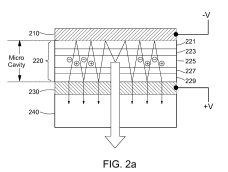
FIGURE 2a describes the structure of an organic light emitting diode
according to the invention. In such an OLED light is emitted downward, i.e.,
through a transparent substrate (240) made for example of glass which also
provides a mechanical support to the device. The metal anode (230) is
CA 02712251 2010-07-14
WO 2009/090248 PCT/EP2009/050504
8
deposited directly on the substrate. The anode is, e.g., made of a layer of
silver
(Ag) thin enough (a few tens of nanometers) to be semitransparent in the
wavelength range of the visible light: 400-700 nanometers (nm). The anode
(230) is the lower mirror of the microcavity (220) that will be formed after
deposition of the upper electrode (210).
Optionally, as shown in Figure 2b, the anode may also include a layer
of transparent ITO (232) previously deposited by sputtering on the substrate
(240). Although this is not mandatory, this helps further reducing the sheet
resistance of the anode if necessary, e.g., for the fabrication of very large
devices or for devices having a form factor detrimental for the electrical
properties. Together, the layer of silver (231) and the underlying layer of
transparent ITO (232) then constitute the anode (230). Because ITO is
deposited first on the glass substrate, prior to the thermal vacuum deposition
of
the organic layers, they cannot be disturbed by the sputtering processing
step.
Hence, this alternate fabrication process of a bottom-emitting OLED remains
compatible with the objects of the invention.
The upper electrode (210), i.e., the cathode of the device is made, e.g.,
by thermal vacuum deposition of aluminum or silver thick enough to be fully
reflective (several hundred nanometers).
Between the anode (230) and cathode (210), the successive following
layers of organic materials are deposited in a vacuum chamber by thermal
evaporation:
- The first organic layer (229), a few tens of nanometers thick, is used to
facilitate transport of holes that are injected by the anode (230) when this
latter
is tied to a positive voltage. It is placed immediately above the anode. The
material is doped (P-type doping) to enhance conduction by holes (i.e.: by
lack
of electrons). In conjunction with the layer of silver below, and optionally
that of
ITO (232) the electrical resistance of the anode layer (230) may be very low.
- The following organic layer (227) with a thickness of about ten nanometers
is
used to block the electrons that could come from the upper layers and would
recombine otherwise in the underlying organic layer used to facilitate
transport
of holes (instead of normally recombining in the electroluminescent layer).
CA 02712251 2010-07-14
WO 2009/090248 PCT/EP2009/050504
9
- The middle layer (225) is the organic layer where electrons and holes
recombine and from where light is emitted. The thickness depends on the
material used according to the color of light to emit.
- The layer (223) located directly above the light-emitting layer is used to
block
the holes coming from the lower layers. This layer plays a role equivalent of
that
of layer (227) which serves to block electrons. It is about of the same
thickness.
Together, the blocking layers help to confine the recombination of electron-
hole
pairs in the intermediate light-emitting layer (225).
- The top organic layer (221) is used to facilitate the transport of electrons
that
are injected by the cathode when tied to a negative voltage. The material is
doped (N-type doping) to enhance a conduction by excess of electrons. In
conjunction with the metal layer forming the reflecting cathode (210) the
electrical sheet resistance is very low and independent of its thickness. Like
the
lower doped layer its thickness is below a few tens of nanometers.
The structure of the above organic layers (omitting the blocking layers
of electrons and holes) which combines: a P-type doped layer, a non-doped
(intrinsic) layer made of a luminescent material, and an N-type doped layer,
is
said to form a PIN structure. The materials used for this organic structure,
doped or not, must have preferably a same refractive index (close to 1.7) in
order not to create internal reflections that would affect the transmission of
the
light emitted from the intermediate light-emitting layer (225). All these
materials
are commercially available. They can easily be deposited by vacuum thermal
evaporation.
Following gives a list of commercially available materials that can be
used to realize OLEDs according to the invention:
Meotpd: N,_N,_N',_N'-_tetrakis_(4-_methoxyphenyl)_benzidine
Bphen: 4,7-_Diphenyl-_1,10-_phenanthroline
Cs: cesium
alpha-NPD: N,N'-Di(napthalen- 2-yl)-N,N'-diphenyl-benzidine
F4tcnQ: tetracyanoquinodimethane
Ir(PIQ)3: tris(1-phenylisoquinoline) iridium
CA 02712251 2010-07-14
WO 2009/090248 PCT/EP2009/050504
Above materials are used as indicated in following exemplary OLED
structure:
Substrate: Glass.
Anode: Ag layer, 33 nm thick.
P-Transport: Meotpd layer doped with F4tcnQ in a ratio of 4%,
total thickness: 38 nm.
N-Blocking: pure Meotpd, 10 nm thick.
Light-emission: alpha-NPD layer doped with lr(PIQ)3 in a ratio of 15%,
(in the red) total thickness: 20 nm.
P-Blocking: pure Bphen layer, 10 nm thick.
N-Transport: Bphen layer doped with Cs in a ratio of one atom of Cs for
one molecule of Bphen, giving to the layer a conductivity of
about 10-5 Siemens/cm.
Cathode: Ag layer, 150 nm thick.
While doping of the organic layers cannot explain alone the observed
improvement of luminance efficiency the use of doped transport layers indeed
5 allows sheet resistance of these layers to remain low even though they need
to
be thin. Hence, the thickness of the layers can be freely adjusted to enhance
the optical properties of OLEDs in order to obtain a microcavity (220) best
adapted for the light color to generate. Thus, the height of the microcavity
(220)
can be adjusted so that a resonance occurs for the wavelength of the light to
10 emit. In addition, the light-emitting layer (225) can be vertically placed
(that is
with an orientation according to the height of the micro cavity) exactly where
within the microcavity (220) it produces a maximum of light. This is achieved
by
independently controlling thickness of each of the different layers forming
the
organic structure; mainly the P and N doped layers (221, 229). This can be
done irrespective of the electrical parameters, i.e., the sheet resistance of
the
cathode (210) and of the anode (230) which can be kept low due to the use of
doped organic materials so that voltage drops and heat dissipation remain
negligible. Moreover, the deposition of a doped organic layer directly on the
anode metal does not create a barrier to the injection of holes unlike the
case of
the deposition of an intrinsic organic material as reported in the background
section. The same applies to the injection of electrons in the doped area from
the cathode. This is a major contributor to obtaining high luminance
efficiency.
CA 02712251 2010-07-14
WO 2009/090248 PCT/EP2009/050504
11
All layers, organic and metallic, are advantageously deposited by
vacuum thermal evaporation of corresponding materials.
FIGURE 3 illustrates the action of the microcavity on the reduction of
the range of wavelengths emitted by a device as described in the previous
figures (2a and 2b). The reflectivity of such a layered system can be analyzed
so as to obtain an optimal optical setting of the organic and metallic layers.
Figure 3 shows the results obtained with an aluminum cathode (320) and a
silver cathode (330). In both cases the semi transparent anode is made of
silver. The silver cathode gives a narrower spectrum of color closer to
producing
a pure primary color, red in this case, with a minimum reflectivity of the
layered
structure close to 610 nm (and thus a maximum transmission for that color).
Figure 3 also shows the reflectivity of a comparable structure (310) that does
not benefit of the action of the microcavity though. This would be the case of
a
device as described in Figure 2 but without the semi reflective anode. This is
obtained, for example, by replacing silver, or the couple silver-ITO, by ITO.
No
reduction of the range of emitted wavelengths is then observed.
FIGURE 4 shows the results obtained with an OLED structure of the
invention as described in Figure 2. This serves to illustrate the magnitude of
the
technical progress achieved. The curves plot the luminance output efficiency,
in
candela per ampere (Cd/A), obtained as a function of the luminance level
reached, in candela per square meters (Cd/m2). The best luminance efficiency
figure is obtained with a device having a silver cathode (410). The one with
an
aluminum cathode (420) has a luminance efficiency figure of half the value. As
far as the comparison device (430) is concerned, the one without microcavity,
it
is significantly worse.
CA 02712251 2010-07-14
WO 2009/090248 PCT/EP2009/050504
12
The following table also shows what voltages must be applied between
anode and cathode to obtain the reported luminance output efficiency for two
standard values of luminance level.
Voltage (volt) Voltage (volt) Max luminance
at 1.000 Cd/m2 at 10.000 Cd/m2 efficiency in Cd/A
No microcavity 2.77 3.6 7.5
Aluminum cathode 2.5 2.8 19
Silver cathode 2.65 2.9 42
Voltages necessary to operate an OLED of the type of Figure 2 are fully
compatible with the standard values of power supplies used by the
microelectronics industry (3-5 volts). The maximum luminance efficiency
obtained in the red (42 Cd/A) with the OLED structure using a silver cathode
is
close to the best results reported for devices emitting in the green and is
significantly better than any previous results reported for OLEDs emitting in
the
red.