Note: Descriptions are shown in the official language in which they were submitted.
CA 02713369 2010-07-21
WO 2009/109714
PCT/FR2009/000063
1
POWER RECTIFYING CIRCUIT AND SYSTEMS, ASSOCIATED METHOD,
AND AIRCRAFT INCLUDING SUCH CIRCUIT OR SYSTEMS
The present invention relates to a power rectifying device and
method, to an associated system and to an aircraft comprising such a device
and/or system.
In the field of conversion and regulation of electrical energy by
electronic power circuits, numerous applications require a functionality of
alternating current/direct current (AC/DC) rectifier type in which the AC side
performs sinusoidal sampling of the current in phase with the voltages of the
supply network, in order to optimize the power factor as close as possible to
1 and to obtain an optimum energy efficiency and/or to satisfy the quality
standards of the distribution network. The DC side constitutes the output of
such circuits. The AC supply side of such an alternating current network may
be, for example, an electricity generating system installed on board an
aircraft to supply an on-board network, such as described in applications FR
2881896 and FR 2897731. In particular, the DC stage may itself supply a
DC/DC or DC/AC converter, such as a motor-inverter assembly or an
emergency power supply.
The developments in power electronics have drawn attention to the
performances of AC/DC converters based on active switched-mode rectifiers
associated with pulse width modulation techniques (PWM, acronym for
"Pulse Width Modulation" according to English terminology). These circuits
are essentially based on power semiconductors, in which the pulse
modulation makes it possible to control the flow of power drawn from the
alternating current network. These circuits also make it possible to regulate
the continuous DC voltage at the output, especially with a view to supplying
other DC/DC or DC/AC converters.
Solutions known heretofore exhibit two-level voltage modulation,
consequently having the disadvantage of necessitating high-inductance
inductors on the AC side and a large weight penalty.
CA 02713369 2010-07-21
WO 2009/109714 PC
T/FR2009/000063
2
Known solutions use what are known as "standardized" symmetric
commutation cells, in the form of a voltage inverter, equipped with two
transistor-diode assemblies (dual transistor-diode) controlled by PWM
generators. For example, there are known two transistor-diodes in series on a
source of DC voltage E.
Such circuits have the advantage of being versatile and modular, but
they still become rapidly complex because of the large number of transistors
and of electronic control signals applied to the transistors. In addition,
these
systems appear to be less reliable than a passive diode-type rectifier and
they
have clearly larger power losses by reason of the presence of twice as many
components, which on average generate additional losses due to the high-
frequency commutations and high voltage rating of components, typically 1200
V, in industry.
Furthermore, these systems are based on voltage switching at two levels
(in other words, offering two DC voltage levels from the AC side: -E/2 V and
E/2
V), necessitating the use, at the rectifier input, of AC smoothing inductors
having sufficiently high inductance to correspond to the volt-seconds
(proportional to the voltage E multiplied by the switching period Tdec, where
E
denotes the DC voltage and Tdec (or Fdec) represents the switching period (or
frequency)). This results in a large penalty in terms of weight and volume.
In these traditional circuits, the commutation cells are composed of two
transistors in series. A low-impedance failure (or short circuit) of one of
these
results in short-circuiting of the DC bus, in which a large amount of energy
may
be stored, in particular several hundreds of joules. This energy may be
sufficient to lead to explosion of housings unless rapid protection is
activated on
the transistors.
Even in the presence of this protection, this type of fault may propagate
to the supply network and to other adjacent cells of the circuit, which
necessitates adding supplementary isolating and redundant devices to the
, =
CA 02713369 2010-07-21
,
WO 2009/109714
PCT/FR2009/000063
3
circuit to safeguard the failed portion of the circuit and to continue energy
management in emergency mode.
The resulting circuits then rapidly exhibit configurations that are more
complex, more costly and probably associated with a risk of loss of
reliability
compared with a simple passive diode-type rectifier.
A need therefore exists to have fault-tolerant rectifying circuits, at once
trustworthy, efficient from the viewpoint of volt-seconds applied to the
inductors,
and using switches of low voltage rating.
Some of the above disadvantages disappear when the interest lies in the
particular case in which power reversibility is not required, is prohibited or
impossible, for example in the case in which the initial supply network is of
alternating current type in view of supplying a unidirectional direct current
bus
with power. An on-board network in an aircraft generally exhibits these
characteristics, where an alternating current generator is delivering
electrical
energy to the entire aircraft.
In the absence of reversibility, the switching circuits are simplified, the
commutation cells are no longer able to be reversible in current and then
comprise no more than a single transistor and a single diode, therefore a
reduced number of transistors and of means for controlling the transistors.
This
results in a lower cost, reduced risks of faults in the control circuit and
smaller
power losses. Such circuits are therefore adapted for applications/equipment
requiring power over a broad range and industrial voltages, such as 300 V to
1200 V, typically 800 V.
The circuits obtained in this way are traditionally known as PCF circuits
("Power Factor Correction", or correction of the power factor) or as "boost"
(step-up) rectifiers with sinusoidal sampling.
In the case of a three-phase supply, the boost rectifiers are based on a
bridge of six diodes or three branches of rectifiers comprising 2 or 4 diodes
(for
all of the three phases of the supply source) associated with a single or
double
boost circuit. On Figure 1 there has been shown a double boost circuit
CA 02713369 2010-07-21
,
WO 2009/109714
PCT/FR2009/000063
4
equipped with a 2-diode rectifier and exhibiting three voltage levels on the
AC
side, which makes it possible to divide the volt-seconds dimensioning the
inductors by 2. This circuit is described in particular in the Barbosa
dissertation
("Three-Phase Power Factor Correction Circuits for Low-Cost Distributed Power
Systems", Peter Mantovanelli Barbosa ¨ report of Dissertation defended at the
Faculty of the Virginia Polytechnic Institute and State University, July 31,
2002,
Blacksburg, Virginia).
Two unidirectional current boost cells 10 and 11 are seen, each
connected to alternating current supply 12 by rectifying diodes 13 and 14 and
an inductor 15. Each boost cell is composed of a diode 100 or 110, a switch
102 or 112 and a capacitor 104 or 114 (defining a continuous DC voltage bus).
Hereinafter the terms "component of a boost cell" and "boost component" will
be
used synonymously, for example for a boost diode.
This circuit functions at a switching frequency Fdec corresponding to the
repeat frequency of the control instructions to the transistor switches.
These solutions provide a simplification of switching circuits
accompanied by a decrease in inductance of input inductors 15, especially by
virtue of the appearance of a third level (in this case the voltage levels -
E/2, 0
and E/2 are obtained on the AC side), which makes it possible to use inductors
having inductance reduced by half.
The withstand voltage of the assembly of components (boost diodes and
transistors) is also reduced by half, and the rating of these components,
including tolerance margins, is reduced by the same proportion, from 1200 V to
600 V.
The circuit of Figure 1 is already a first step toward greater operating
safety. In fact, any fault in one of the two transistors is spontaneously
isolated
by the boost diodes. In this way short circuiting of the DC bus is avoided in
such
a scenario.
Nevertheless, the fault propagates to the AC phase, necessitating
isolation, for example by fusible link or thyristor.
CA 02713369 2010-07-21
,
WO 2009/109714
PCT/FR2009/000063
It nevertheless is noted that the isolation of one of the two boost cells
causes the circuit to function only during a single half period of the input
wave
from the AC side.
A solution to this limitation is known, in particular from patent application
FR 2809548, which introduces a topological redundancy by describing a multi-
level boost rectifying circuit, one particular case of which has five levels.
Two
equivalent diagrams illustrating the topology of this known rectifying circuit
have
been shown on Figures 2a and 2b.
This circuit comprises four boost cells 20 to 23. The first stage, formed
by cells 20 and 21, has the same topology as the circuit of Figure 1 (in the
absence of rectifying diodes 13 and 14). A second identical stage (cells 22
and
23) has been added downstream from the first stage, in this way creating five
output voltage levels in total on the AC side: -E/2; -E/4; 0; E/4; E/2.
It is seen that the addition of an identical stage in cascade makes it
possible to reduce the rating by 2 and to use only standard voltages of 600 V.
The presence of the second stage makes it possible to double the
switching frequency to 2.Fdec. In this way frequencies up to a few hundred
kilohertz are possible, permitting an increase of the useful pass band if the
AC
network is of high frequency, and a decrease of the volt-seconds applied to
the
inductors entails a reduction in the dimensions of the passive components,
especially of input inductor 15. This reduction makes it possible in
particular to
apply reduced voltages to the components for a given supply voltage and
therefore to under-dimension the components (economic benefits) or, at the
same rating, to accept much higher supply voltages.
The increased switching frequency also makes it possible to decrease
the capacitance of the capacitors in the boost cells, with the consequence
that a
smaller amount of energy is stored in the circuit. Thus, when a boost diode
breaks down and the transistor of the cell causes the capacitor to be short-
circuited, the risk of explosion is rapidly averted.
In addition, when a transistor breaks down, the circuit is safeguarded by
CA 02713369 2010-07-21
,
WO 2009/109714
PCT/FR2009/000063
6
the presence of the boost diode and the energy is dissipated by recycling to
the
AC sources. In this way the safety of such a system is increased.
This solution also has the advantage of being fault-tolerant. In fact, in the
case of a fault of a transistor switch, for example that of cell 20, the other
stage,
in this case cell 22, continues to switch, now at the switching frequency Fdec
(because it keeps on switching during the active half cycle of the supply
current
despite the failed cell). In the case of failure of a switch, one output
voltage level
thus is lost, at the cost of a static overvoltage (that is to say at the
terminals of
the diodes) of 50% and a dynamic overvoltage (that is to say at the terminals
of
the switches/transistors) of 100%, and a single switching frequency results
for
the upper or lower part affected by this failure.
It is seen that, in this solution, the diodes in boost cells 20 to 23 must be
dimensioned for the totality of differential voltages of the cell, therefore
for a
voltage rating equal to E/2 (E/4 + E/4 for the first stage and E/2 + E/2 - E/4
- E/4
for the second stage). Thus, for an output voltage of E = 800 V applied in
industry, it is advisable to use diodes having a rating of at least 400 V, or
generally 600 V, including a margin.
However, this solution has the disadvantage that, in case of failure of
switches, the diodes of the boost cells are subjected to a static voltage of
3E/4
(+ 50%), or in other words, 600 V, in the above example, and to a dynamic
voltage of E/2 (+ 100%), or in other words 400 V. Thus, in the presence of
diodes rated at 600 V, including a safety margin, the circuit is not fault-
tolerant.
Thus, to achieve fault tolerance, it then is indispensable to dimension the
components for at least 600 V (that is to say without margin), in particular
to
dimension the diodes for at least 800 V, including a margin, or in other words
beyond the output voltages E/2 being used.
To avoid limiting the functioning to 600 V, a voltage rating of 800 or even
1200 V is therefore necessary, but adversely affects the performances in
CA 02713369 2010-07-21
, .
WO 2009/109714
PCT/FR2009/000063
7
commutation speed, voltage drop and power loss of the diodes.
In addition, another disadvantage of this structure lies in the fact that the
commutation cells contain one diode and two transistor-diode pairs, one of
these pairs being static. That leads to higher parasitic inductances than in
the
foregoing circuits.
With regard to these disadvantages, it is sought to obtain a power
rectifying circuit that is intrinsically ¨ that is to say without addition of
supplementary circuits ¨ tolerant to failures of switches and diodes and that
requires diodes and switches (transistors) of lower rating for the same output
voltages.
The invention aims in particular to overcome these disadvantages by
providing a multi-level fault-tolerant voltage rectifying circuit comprising
boost
cells, especially with a single transistor and a single diode per cell.
In particular, a boost cell assures switching despite the internal failure of
another boost cell, which guarantees tolerance to failures of switches or
diodes.
In addition, the circuit according to the invention makes it possible to
have the diodes function at a voltage of E/4 (that is to say 200 V for an 800
V
voltage source) and thus to require, in the case of failure, a rating of E/2
(that is
to say 400 V), or in other words the output voltage. Thus components rated at
600 V are possible with a reasonable operating margin.
For this purpose, the invention aims in particular at a power rectifying
circuit for an electrical current signal (or wave) delivered by an alternating
current source, comprising:
¨ two separate commutation assemblies arranged to be connected to a
supply terminal of the source, at least one commutation assembly comprising a
plurality of commutation cells, referred to as boost cells, in cascade,
¨ each boost cell comprising a diode connected between a first input
terminal and a first output terminal of the cell, a switch means connected
between a second input terminal and a second output terminal of the cell, and
a
capacitor connected between the two output terminals of the cell,
CA 02713369 2015-11-26
8
¨ the boost cells of a commutation assembly being arranged in cascade
so that the first and second output terminals of one boost cell are connected
respectively to the first and second input terminals of the following boost
cell,
¨ the capacitors, known as terminal capacitors, of the two terminal boost
cells (of the cascade) of the assemblies having one terminal in common.
The invention also applies to power rectifying circuit for electrical current
delivered by an alternating current source, comprising: two separate
commutation assemblies arranged to be connected to a supply terminal of a
source, at least one commutation assembly comprising a plurality of
commutation boost cells in cascade; each boost cell comprising a diode
connected between a first input terminal and a first output terminal of the
cell, a
switch means connected between a second input terminal and a second output
terminal of the cell, and a capacitor connected between the two output
terminals of the cell, the plurality of commutation boost cells of at least
one of
the commutation assemblies being arranged in cascade so that the first and
second output terminals of one boost cell are connected respectively to the
first
and second input terminals of the following boost cell, the capacitors of the
two
terminal boost cells of the commutation assemblies having one terminal in
common, wherein the power rectifying circuit further comprises blocking means
for blocking all the switch means of the circuit in case of detection of a low-
impedance fault in one of the boost cells, and the power rectifying circuit
further
comprises means for detecting a low-impedance fault in a boost cell arranged
to detect a voltage at terminals of the switch means of the cell during a
predetermined time interval following a control signal to start the switch
means
to detect a fault of the boost diode of the cell or following a control signal
to
block the switch means to detect a fault of the switch means.
In particular, the common terminal is the second output for each of the
commutation assemblies.
The concept of input/output of the cells such as used above is
independent of the direction of the current passing through the circuit,
especially because one of the commutation assemblies is traversed in a
direction inverse to the other, even though they have a substantially
symmetric
structure.
CA 02713369 2015-11-26
8a
By "separate" there is understood the fact that, for each of the
commutation assemblies, the corresponding boost cells (that is to say those of
the same stage within the meaning of Figures 2a and 2b) of the upper part
(first commutation assembly) and of the lower part (second assembly) do not
share components. This results in the absence of voltage constraint ("stress"
according to English terminology) for the components between the assemblies
and therefore in better containment.
This "separation" of the commutation assemblies also makes it possible
to decrease the thermal coupling of the circuit compared with that of Figure
2b.
In fact, in the latter, the two transistor/diode pairs, one of which is
static, require
that they be positioned in geographically close manner in order to create the
minimum of parasitic inductance. The reverse of this necessity is a large
thermal coupling of these two pairs, which disappears by virtue of the
invention.
In contrast to the prior art circuits, the invention also makes it possible to
use transistor switches and diodes in the boost cells at a voltage of E/4 or
in
other words 200 V, in the above example, for a configuration of 2 x 2 cells.
In
case of failure, the diodes of the boost cells are at most subjected to
voltages
of E/2, or in other words the output voltage. Thus, by reducing the rating by
a
factor of 2 compared with the known solutions, faster components having fewer
CA 02713369 2010-07-21
,
WO 2009/109714
PCT/FR2009/000063
9
power losses are obtained.
The switching frequency and the number of voltages on the AC side are
multiplied, especially according to the number of imbricated cells, that is to
say
the number of stages or groups. In this way the volt-seconds applied to the
input inductor (and therefore the size thereof) and the silicon-commutated
volt-
amperes VA can be effectively reduced compared with the prior art, where the
silicon-commutated VA are defined as the sum of the products of the voltage at
the terminals multiplied by the current flowing in each of the transistor
switches
of the cells of the circuit.
In particular, in its configuration of 2 x 2 cells, the invention makes it
possible, with the same number of transistors, that is to say the same level
of
complexity, to divide the value of the input inductance by a factor of 2 to 8,
the
silicon-commutated volt-amperes by a factor of 2, and ultimately to reduce the
losses compared with the prior art solutions by approximately 30%.
Thus it is provided that each commutation assembly can comprise two
boost cells. This configuration offers a good compromise between a small input
inductance and a reasonable number of transistors, thus limiting the total
stored
energy (compared with the presence of N boost cells, or in other words 2 N
capacitors if N >> 2).
Alternatively, it is possible for a commutation assembly to comprise more
than two boost cells. It is specified here that an overly high number of
transistors would increase, the amount of energy stored on average in the
circuit. Thus a maximum of five boost cells, typically from 2 to 3, is
provided per
commutation assembly.
It is also contemplated to have a different number of cells between the
two commutation assemblies. It is noted that this configuration corresponds to
operating situations in which a certain number of cells have failed in the
assembly having the fewest cells. In particular, the minimalist configuration
provides one commutation assembly equipped with a single boost cell and the
other commutation assembly equipped with two boost cells. This circuit is
CA 02713369 2010-07-21
WO 2009/109714
PC T/FR2009/000063
therefore fault-tolerant in one of the two boost cells of the same assembly
and
has diodes of reduced rating in these two same cells (that is to say a rating
of
only 600 V).
For balanced operation, however, it will be preferred to have an identical
number of boost cells in each of the commutation assemblies.
In order to make the circuit more resistant to failures, it is possible to
provide for the use of redundant cells or assemblies. In particular, it is
possible
to add a redundant cell in one or in each of the commutation assemblies, this
redundant boost cell being passive, that is to say in standby state
(transistor
switch continuously held in conducting state) during the operation of the
other
cells. Upon detection of failure of one cell, the failed cell is substituted
by this
redundant cell. Depending on the position of the latter in the commutation
assembly, it will be advisable to synchronize the control signals of the
switches
with the position of each of the cells operating within the commutation
assembly.
Redundancy may also be applied to a commutation assembly, which will
substitute for one of the two initial commutation assemblies in case of
failure of
too many boost cells, so that switching can no longer be continued. It will be
possible to change the commutation assembly over to the redundant assembly
by the use, for example, of a switch.
It is provided that the circuit comprises rectifying means.
In one embodiment, the rectifying means comprise a pair of rectifying
means arranged to be connected between the said supply terminal and
respectively each of the said commutation assemblies, so as to rectify the low-
frequency input current.
Alternatively, it is conceivable that the rectifying means comprise
rectifying diodes provided in each boost cell, these rectifying diodes being
in
series with the said switch means and conducting in the direction opposite to
that of the corresponding boost diode (that is to say that of the same cell).
Returning to the first alternative above, since the boost cells are
CA 02713369 2010-07-21
WO 2009/109714
PC T/FR2009/000063
11
unidirectional in current (the commutation assemblies also being
unidirectional
by placing the boost cells in series in the same conducting direction), this
configuration makes it possible to protect each of the commutation assemblies
from inverse currents delivered during one half period of alternating current
supply (a half period in which the other commutation assembly is under load).
To this end, it is provided that the system is arranged to force the
commutation
means (transistors) of one commutation assembly to the conducting state while
the other assembly is active.
In particular, each rectifying means comprises a diode, especially
connected in series in the same conducting direction as the diodes of the
commutation assembly to which it is connected.
Alternatively, each rectifying means comprises a thyristor, especially
connected in series in the same conducting direction as the diodes of the
commutation assembly to which it is connected.
By virtue of the use of a thyristor, it is possible to isolate one of the
commutation assemblies in case of a fault in all of the cells of this
assembly.
In addition, the thyristor has the merit of providing current control during
the phase of precharging of the boost capacitors (at E/2 or E/4 in the
configuration of 2 x 2 cells), especially upon startup of the system
comprising
the circuit.
It is provided in particular that these rectifying means are connected in
series in the same conducting direction as the diodes of the commutation
assembly to which they are respectively connected.
In one embodiment, the switch means comprise controlled transistors.
In one embodiment, the circuit comprises blocking means capable of
blocking all the switch means of the said device in case of detection of a low-
impedance fault in one of the boost cells.
In particular, detection may be achieved on the floating capacitors (at the
CA 02713369 2010-07-21
WO 2009/109714
PCT/FR2009/000063
12
output of each boost cell) or on the switch means.
The detection of these faults concerns a general problem, which can be
dissociated from the inventive elements described above. In this design, and
for
the reasons explained below in the description, it will be possible to
envision
protecting, in separate manner, the solution of detection of a fault in a
commutation cell in which two controlled switches are not available.
Thus it is possible for the circuit to comprise means for detecting a low-
impedance fault in a boost cell arranged to detect the voltage at the
terminals of
the switch means of the cell during a predetermined time interval following a
control signal to start the switch means in order to detect a fault of the
boost
diode of the cell or following a control signal to block the switch means in
order
to detect a fault of the said switch means.
In particular, the said means for detecting a low-impedance fault
comprise a transistor controller coupled with a voltage detector.
According to a particular characteristic of the invention, it is provided that
the circuit comprises a supply terminal arranged to be connected to the supply
source.
The invention also applies to a power rectifying system for the electrical
current delivered by a multi-phase alternating current supply source,
comprising
a plurality of power rectifying circuits as presented above and arranged such
that each can be connected to a supply terminal connected to respectively each
of the phases of the multi-phase current, and in which the circuits share the
same terminal capacitors.
In this way there is obtained a system capable of rectifying a multi-phase
current, and generally a two-phase or three-phase current.
The invention also applies to a power rectifying system for electrical
current delivered by an alternating current source, comprising two
corresponding power rectifying circuits as presented above and arranged to be
connected respectively to each of the terminals of the supply source, and in
= CA 02713369 2010-07-21
=
WO 2009/109714
PCT/FR2009/000063
13
which the circuits share the same terminal capacitors.
In this way a system based on the differential voltage at the terminals of
the supply source is obtained.
In particular, it is possible to provide that one cell of one of the
rectifying
circuits and the corresponding cell of the other circuit (that is to say
having the
same relative position in each of the rectifying circuits) share the same
capacitor.
In an embodiment in which a large number of circuit components are
mutualized, it is provided that the two circuits are combined to the exclusion
of
rectifying means provided between each of the commutation assemblies and
the two terminals of the source, the said rectifying means connected to a
given
commutation assembly being exclusive, in opposite directions of current flow.
In this way the number of components of the differential circuit and the
associated losses are reduced.
Of course, if several phases are available on the source, this system is
combined with that presented above for a multi-phase alternating current
supply
source. In particular, in the case of a three-phase supply, the differential
voltage
configuration requires six rectifying circuits such as presented above (2
circuits
for the differential voltage of each of the 3 phases), all sharing the same
two
terminal capacitors.
The invention also applies to a power rectifying method for an electrical
current signal delivered by an alternating current supply source, the method
being achieved by a rectifying circuit comprising:
- two separate commutation assemblies arranged to be connected to a
supply terminal of the source, at least one commutation assembly
comprising a plurality of commutation cells, known as boost cells, in
cascade,
- each boost cell comprising a diode connected between a first input
terminal and a first output terminal of the cell, a switch means connected
CA 02713369 2015-11-26
14
between a second input terminal and a second output terminal of the
cell, and a capacitor connected between the two output terminals of the
cell,
- the boost cells of a commutation assembly being arranged in cascade so
that the first and second output terminals of one boost cell are connected
respectively to the first and second input terminals of the following boost
cell, and
- the capacitors, known as terminal capacitors, of the two terminal boost
cells of the assemblies having one common terminal,
the method comprising a step of sequential control of each of the said
switch means so as to deliver DC voltages to the terminals of the terminal
capacitors.
The invention also applied to power rectifying method for an electrical
current signal delivered by an alternating current supply source, the method
being achieved by a rectifying circuit comprising: two separate commutation
assemblies arranged to be connected to a supply terminal of the source, at
least one commutation assembly comprising a plurality of commutation boost
cells in cascade, each boost cell comprising a diode connected between a first
input terminal and a first output terminal of the cell, a switch means
connected
between a second input terminal and a second output terminal of the cell, and
a
capacitor connected between the two output terminals of the cell, the boost
cells of at least one of the commutation assemblies being arranged in cascade
so that the first and second output terminals of a boost cell are connected
respectively to the first and second input terminals of the following boost
cell,
and the capacitors of the two terminal boost cells of the assemblies having
one
common terminal, the method comprising sequential control of each of the
switch means so as to deliver DC voltages to the terminals of the terminal
capacitors, the method comprising blocking all the switch means of the circuit
in
case of detection of a low-impedance fault in one of the boost cells, and the
method comprising detecting a low-impedance fault in a boost cell arranged to
detect a voltage at terminals of the switch means of the cell during a
predetermined time interval following a control signal to start the switch
means
CA 02713369 2015-11-26
14a
to detect a fault of the boost diode of the cell or following a control signal
to
block the switch means to detect a fault of the switch means.
In one embodiment, the method comprises a step of detecting a low-
impedance fault (or short circuit) in at least one of the said boost cells,
and,
after the said detection, a step of blocking the said switch means of the
boost
cells. Blocking consists in changing the switch means into a blocking / closed
position, as opposed to the conducting / open position of the switches. In
this
way it is possible to apply a blocking policy starting from a certain number
of
faults affecting the boost cells, as defined below.
In one embodiment, the switch means of a commutation assembly are
forced to conducting state when the other commutation assembly is active over
one half cycle of the input current. In this way the application of inverse
voltages
at the terminals of the transistors is prevented.
Optionally, the method may comprise steps and employ means relating
to the circuit and system characteristics presented above.
The invention also applies to an aircraft comprising a device or a system
according to any one of the configurations presented above.
The characteristics and advantages of the present invention will become
more clearly apparent upon reading a preferred embodiment illustrated by the
attached drawings, wherein:
CA 02713369 2010-07-21
WO 2009/109714
PCT/FR2009/000063
¨ Figure 1 shows a prior art double-boost, three-level AC/DC circuit;
¨ Figures 2a and 2b are two equivalent representations of a prior art
multi-level rectifying circuit of SMC type;
¨ Figures 3a and 3b are two equivalent representations of an exemplary
embodiment of the power rectifying circuit according to the present invention;
¨ Figure 4 illustrates the electrical behavior of the circuit of Figures 3
in
case of a low-impedance fault of one of the switches (transistors) of which it
is
composed;
¨ Figure 5 illustrates the electrical behavior of the circuit of Figures 3
in
case of blocking of the circuit following a low-impedance fault of one of the
switches;
¨ Figure 6 illustrates an exemplary differential power rectifying circuit
using the circuit of Figures 3;
¨ Figure 6a shows a particular configuration of the circuit of Figure 6, in
which maximum mutualization of the components is effected;
¨ Figure 7 illustrates an exemplary power rectifying system for a three-
phase supply using the circuit of Figures 3; and
¨ Figures 8a and 8b respectively illustrate a means for detection of a
low-impedance failure at the terminals of a transistor of Figures 3 and the
voltage at the terminals of this transistor for detecting this failure.
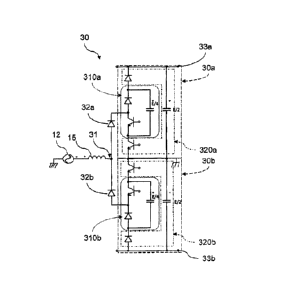
As already stated above, an exemplary embodiment of rectifying circuit
30 according to the invention and such as illustrated by Figures 3 is based on
the "double-boost three-level AC/DC" commutation circuit presented in Figure
1.
An exemplary rectifier having 2 x 2 imbricated cells (310a, 310b, 320a,
320b) making it possible to change from 3 to 5 levels and from switching
frequency Fdec to 2 x Fdec compared with the circuit of Figure 1 has been
shown.
The circuit of Figures 3 is applicable to a non-differential input voltage.
There is an alternating current source 12 connected to an input inductor 15
CA 02713369 2010-07-21
WO 2009/109714
PCT/FR2009/000063
16
forming a supply terminal 31 for the power rectifying circuit.
In detail, on the basis of the two boost cells of the circuit of Figure 1,
circuit 30 has two separate commutation assemblies 30a and 30b, each
connected to supply terminal 31 by a rectifying means, in this case rectifying
diodes 32a and 32b.
Each of the assemblies 30a and 30b is unidirectional, in that they allow
current to flow in one direction only. Furthermore, the two assemblies exhibit
opposite directions of current flow.
Rectifying diodes 32a and 32b are conducting in the same direction as
commutation assemblies 30a and 30b, to which they are respectively
connected.
Each commutation assembly 30i is composed of at least two boost cells,
in this case two, 310i and 320i (i = a, b), themselves composed of a diode
312i/322i, a semiconductor controlled switch (314i/324i) of transistor type
and a
capacitor 3161/326i. The diodes 312i/322i of a given assembly 30i are arranged
in the same conducting direction.
Each cell of a stage j is connected to a cell of a stage j + 1 by connecting
the diode and switch of cell j + 1 to the respective terminals of capacitor j.
It is noted that a boost cell of a stage j does not have a part or
component in common with the boost cell of the same stage j in the other
commutation assembly. This independence assures that no voltage stress
associated with dysfunctioning of one of the cells will affect the cell of the
same
stage j in the other assembly.
Diode 312i and switch 3141 of the cell of first stage 1 are connected to
rectifying diode 32i.
Each capacitor 3261 of the cell of the last stage, in this case stage 2, is
connected to the neutral terminal of AC source 12 (for a non-differential
circuit
as is the case in Figures 3) by its terminal common to switch 324i of the same
cell. Thus these capacitors 326i, known as terminal capacitors, have one
common terminal and are connected in series.
CA 02713369 2010-07-21
WO 2009/109714
PCT/FR2009/000063
17
Each commutation assembly 30i is connected at the output to an output
terminal 33i via the terminal of terminal capacitor 326i which is common to
diode 322i. In this way an equipment item (not shown) to be supplied is
connected to output terminals 33i. In industry it is common practice to use
equipment items functioning at a DC voltage of E = 800 V, a value that is also
being integrated into the next aeronautical standards.
Controlled switches 314i and 324i are driven by one or more control
devices known to those skilled in the art (not shown, for example one device
per stage j). For the circuit containing 2 x 2 boost cells, it is possible to
use
control signals similar to those disclosed in the aforementioned application
FR
2809548 for a supply 12 of the same frequency. For this reason the
mechanisms of charging and discharging of the four capacitors 316i and 326i
by commutation of the four switches 314i and 324i is not described in further
detail.
The circuit therefore makes it possible to obtain voltages on the AC side
(-E/2, -E/4, E/4, E/2) as well as the potential 0 at the common terminal of
terminal capacitors 326i.
This example can now be easily extrapolated to a circuit having 2 x N
cells. Such a resultant circuit also meets the criteria of the invention.
However, it
will be limited to 2 x 5 cells. Beyond this, large overall losses in switches
314i,
324i, etc., associated with the series connection of too many components,
would detract from the circuit performances.
The voltage on the AC side then has 2N + 1 voltage levels: -E/2N,
-E/4, -E/2, 0, E/2, E/4, E/2N.
Referring to Figure 4, the tolerance of the circuit according to the
invention to low-impedance faults now is explained. In this figure, graph 40
shows the currents of the three phases of three-phase source 12 (only one of
these phases is of interest here, that received by the circuit in question)
through
the corresponding input inductors 15; graph 41 shows the voltage at the
terminals of capacitor 316a of the failed cell; and graph 42 shows the power
CA 02713369 2010-07-21
WO 2009/109714
PCT/FR2009/000063
18
(and therefore the voltage, since the current intensity is kept constant by
source
12) stabilized at the output of the circuit from a non-supplied state (t = 0)
to a
stabilized state after the fault (up to t = 20 ms).
Transistor 314a goes into a low-impedance fault, that is to say that it
becomes continuously conducting. In Figure 4, this fault occurs at instant T.
Diode 312a, which is immediately in series, then exhibits a voltage equal
to -E/4 at its terminals. Diode 312a then becomes blocking and isolates the
fault
from the DC continuous bus; only cell 310a concerned is naturally taken out of
service by progressive discharge of floating capacitor 316a.
Capacitor 316a ultimately becomes discharged. The voltage at its
terminals drops gradually to 0 at the instant T + At during each switching
period,
where At is the time necessary for the half cycle in question to pass through
the
failed transistor in order to permit its discharge. In practice, this value
depends
mainly on the characteristics of capacitor 316a. The energy released by this
uncontrolled discharge is returned to the network (source 12).
Diode 312a remains in blocking state, isolating failed boost cell 310a.
It is noted here that, even though switch 314a has failed, cell 310b
functions normally, without a substantial voltage being present at the
terminals
of diode 312b.
With failed cell 310a isolated, switching of the alternating current is
maintained on contiguous cell 320a, by means of an overvoltage corresponding
to a factor of 2 for diode 322a. Nevertheless, this overvoltage is not
necessarily
stressing, by reason of the initial reduction by a factor of 2 in the rating
compared with the prior art, all the more so because the maximum rating
attained is E/2, or in other words the maximum voltage sought at the.output.
This additional load on cell 320a surviving the fault results in particular
from the fact that the electrical current associated with the positive voltage
(half
period of the current half cycle) delivered by source 12 is entirely handled
by
this boost cell 320a.
CA 02713369 2010-07-21
WO 2009/109714 PC
T/FR2009/000063
19
It is noted here that commutation assembly 30b is not affected by this
failure and continues to function at 2.Fdec for each of the two cells 310b and
320b.
Naturally, since capacitor 316a is isolated, circuit 30 works with only 4
voltage levels: -E/2, -E/4, 0 and E/2.
It is noted, however, that the power delivered at the output is kept
relatively constant despite the fault (see graph 42 of Figure 4).
Specifically, at
the instant t + At, there is observed a localized rise in output power
associated
with the fact that, because of the failure, common terminal 31 experiences a
potential drop, leading to an increase of current in the inductor via the
voltage
drop at the terminals of this inductor, and consequently to a power spike.
Capacitor 316a of the failed cell discharges and returns the energy of the
failed cell to the network.
Since the two commutation assemblies 30b are separate, it is also
possible to tolerate a fault in one of the two cells 310b and 320b. In
general, it is
possible that the boost cells of a commutation assembly will fail one after
the
other. Nevertheless, the commutation assembly assures switching over the half
cycle in question of the source current as long as at least one sound cell
remains.
In order to alleviate any failure of the assembly of cells of a given
commutation assembly 30i, it is possible to replace low-frequency rectifying
diode 32i by a thyristor, in order to spontaneously isolate the commutation
assembly upon passage through zero. In this way any short circuit of the
output
bus is avoided.
Referring to Figure 5, another embodiment of the response of the circuit
to a low-impedance fault now is illustrated. This embodiment is applicable in
particular when the overvoltage stress of surviving diode or diodes 324a of a
commutation assembly 320a affected by a failure is disabling, for example by
reason of commutation losses or overvoltages.
Figure 5 again illustrates the circuit (left part) and also presents a graph
CA 02713369 2010-07-21
WO 2009/109714
PCT/FR2009/000063
50 of the three phase currents at the terminals of the corresponding input
inductors 15 and a graph 51 of the voltage at the terminals of the capacitor
of
the failed cell.
As in Figure 4, circuit 30 experiences a low-impedance fault at the
position of controlled transistor 314a at instant T.
In this embodiment, the fault that has occurred is detected first of all.
Referring to Figure 8a, there has been shown a transistor controller 80
coupled with a voltage detector 81 used to detect the faults in one of the
boost
cells. Detection is achieved on the basis of the voltage behavior at the
terminals
of the controlled transistor. Since this circuit is known to those skilled in
the art,
the components are not described in further detail.
The graph of Figure 8b illustrates the voltage at the terminals of
transistor 314a measured by circuit 80-81 (curve 82, where the left part in
bold
illustrates the normal behavior and the lighter parts illustrate erroneous
behavior
permitting detection of a fault) following a control signal to change to the
conducting state (83) and a control signal to change to the blocking state
(84).
As used conventionally, this system makes it possible to detect any fault
of a second component of the boost cell in which the controlled transistor, in
this case 314a, is inserted: in the present case a fault of diode 312a is
detected.
In detail, the voltage at the terminals of transistor 314a is Vce in the
blocking state. At instant 83, the transistor is changed to the conducting
state.
In case of normal operation of the boost cell, the voltage decreases to a
quasi-
zero value (bold curve). In the presence of a fault of adjacent diode 312a,
the
voltage rises to the value Vce after a few ps, typically 5 ps. Thus a delay of
approximately ten ps is provided after control signal 83 in order to detect
whether the resultant voltage at the terminals of transistor 314a has been
modified (normal behavior) or not (failed behavior of the diode).
Nevertheless, the conventional use of this circuit 80 does not permit the
detection of a fault of the same transistor 314a, especially because no need
to
CA 02713369 2010-07-21
WO 2009/109714
PCT/FR2009/000063
21
do so was apparent, from the fact that these circuits 80 were generally used
in
these cells comprising two transistors, which then performed reciprocal
monitoring of one another.
In the absence of a need for detection for the transistor itself, without the
presence of a second transistor having a symmetric role, one object of the
invention provides for achieving the detection of the fault of transistor 314a
following the control signal to change to blocking state 84.
As can be seen in Figure 8b, the normal behavior of the transistor (bold
curve) following control signal 84 tends to a voltage on the order of Vce at
its
terminals.
On the other hand, in the presence of a fault of the transistor, such as a
low-impedance fault, this transistor 314a does not maintain the voltage Vce at
its terminals following control signal 84, but the voltage at the terminals
drops to
a quasi-zero value (light curve).
The delay in detection of the phenomenon is approximately 5 ps. A
detection period of approximately ten ps is therefore provided to determine
whether or not a modification of the voltage at the terminals of the
transistor has
occurred following the application of blocking control signal 84.
By equipping each of the transistors with such a circuit 80 as well as with
ad hoc detection logic, it is thus possible to detect a fault in any
transistor of
circuit 30.
Upon detection of the fault, the control device of the switches blocks all
switches (in operation) of circuit 30, as illustrated by the OFF symbols in
Figure
5. As seen above, detection also may relate to a failure of a diode.
Circuit 30 then corresponds to a single diode rectifier (diode bridge), as
illustrated by graph 51.
This embodiment may be modulated by establishing different policies for
blocking switches that are still functioning, depending on the detection or
detections achieved. In particular, blocking of all switches can be achieved
only
when the number of failed transistors in a given commutation assembly 30i
CA 02713369 2010-07-21
WO 2009/109714
PCT/FR2009/000063
22
reaches a threshold value. Such a value may be predefined theoretically in
order to define a threshold voltage applied to the diodes, taking into account
both the rating of the boost diodes and the number of stages (since the
overvoltage experienced due to a failure depends on the number of stages and
adds to the overvoltage experienced through a second failure in the same
commutation assembly).
In practice, this embodiment is used with a multi-phase, for example
three-phase, supply (see Figure 7). In this case, all the controlled switches
of
the circuit (of one phase) affected by the fault are blocked, and the output
power of the three-phase system is then adjusted by circuits 302 and 303 of
the
(two) other phases, in particular to preserve the regulation of the DC bus.
Referring to Figure 6, the use of the circuit constituting the object of the
invention is now described in a differential approach.
Differential power rectifying system 60 then comprises two circuits 30
and 30', which in particular are identical to the circuit of Figures 3, and
their
supply terminals 31 and 31' are connected respectively to an input impedance
15 and 15', which are connected to the two terminals of alternating current
source 12.
The two circuits 30 and 30' have their output capacitors 326a and 326b
in common, in such a way as to form a single output bus of system 60 between
terminals 33a and 33b.
It is seen here that the commutation assemblies having a common
output capacitor, referred to as "corresponding" commutation assemblies (such
as 30a and 30'a), are not used during the same half cycle of the current of
source 12. It is then provided that the components of two corresponding
assemblies will be mutualized, this mutualization being able to apply to one
or
more components.
In particular, according to a complementary embodiment, it is possible to
envision using common capacitors (316a/b, 316a'/b') for the "corresponding"
boost cells of the two circuits 30 and 30' or connecting the two capacitors
315a/b, 316 a'/b' of the two corresponding cells in parallel (which reduces
the
CA 02713369 2010-07-21
WO 2009/109714
PCT/FR2009/000063
23
size of the capacitors).
Figure 6a presents the case of maximum mutualization, even if
intermediate states of mutualization are provided. In this configuration, the
boost cells of the two circuits 30 and 30' are combined, which leads to a
commensurate reduction of the number of diodes and transistors.
As can be seen in this figure, each commutation assembly 30-30'a, 30-
30'b is connected by the same terminal to the two terminals of the supply via
rectifying diodes positioned in opposite direction. Thus it is seen that the
diodes
connected to a given commutation assembly are mutually exclusive (opposite
conducting direction), so that the commutation assembly is used successively
for each of the two half cycles of the current of source 12 via each of the
two
rectifying diodes.
This configuration thus uses the four controlled transistors continuously,
the applied control signals being offset by 90 (n/2) between these different
transistors.
As indicated in the foregoing, the mutualization may be partial, for
example, a single commutation assembly is mutualized with the corresponding
assembly of the other circuit.
In particular, the differential system obtained in this way has 9 voltage
levels for a control frequency equal to 4.Fdec.
Referring to Figure 7, the use of the circuit constituting the object of the
invention now is described for a multi-phase, in particular a three-phase
source
12, in a non-differential approach.
The power rectifying system for three-phase supply 70 comprises three
circuits 301, 302 and 303, each similar to that of Figures 3, connected
respectively to one phase 121.122, 123 of supply source 12.
The three circuits have their terminal capacitors 326a and 326b in
common, so as to form a single output bus of system 70 between terminals 33a
and 33b.
The modulation of the control signal of the controlled switches of the
CA 02713369 2010-07-21
WO 2009/109714
PCT/FR2009/000063
24
three circuits is similar. In particular, the switches having an identical
position in
each of the three circuits 301, 302 and 303 respectively are controlled by
modulation offset by the same angle as the phases of the supply source, in
this
case substantially 27c/3.
It is also possible to provide a differential power rectifying system for a
multi-phase supply by applying division of the circuits of Figure 6 for each
of
the phases of the system of Figure 7: six circuits 301, 30'1, 302, 30'2, 303
and
30'3 are then obtained.
The foregoing examples are only some embodiments of the invention,
which is not limited thereto.