Note: Descriptions are shown in the official language in which they were submitted.
CA 02713644 2010-07-29
WO 2009/121464 PCT/EP2009/001675
Antenna arrangement having at least two decoupled antenna coils;
RF component for non-contact transmission of energy and data;
electronic device having an RF component
Description:
The invention relates to an antenna arrangement and to an RF component having
such an antenna arrangement. Moreover, the invention relates to an electronic
device having an RF component for contact-free transmission of energy and data
to the electronic device.
It is a known procedure to use antennas in the realm of contact-free energy
and
data transmission. Particularly in contact-free data transmission, RFID (Radio
Frequency Identification) systems are used. Such a system normally consists of
an
RFID chip (transponder/tag) that is attached, for example, to an object, to a
person
or animal, or to a fixed position, and it also consists of one or more reading
and/or
writing devices. The RFID chip can be read and written by the reading and/or
writing device contact-free via high-frequency signals if the RFID chip is
located
within the range of one of these devices.
From a technological point of view, RFID systems and the associated transpond-
ers can differ a great deal from each other. An important differentiation
feature is
the type of energy supply for a transponder. Here, a distinction is made
between
active and passive RFID transponders, whereby active transponders have their
own energy supply, for example, in the form of a battery, while passive trans-
ponders obtain the energy needed for their operation from the radio signal of
a
base station. Normally, passive RFID tags are used whenever the aim is to
attain
the smallest possible sizes at low production costs. In contrast, active
transponders
with their own energy supply are larger and their production entails higher
costs.
CA 02713644 2010-07-29
WO 2009/121464 PCT/EP2009/001675
2
A passive transponder has an antenna, for example, in the form of an antenna
coil
with at least one winding, via which the energy can be drawn from the signal
of a
reading and/or writing device. Battery-free transponders normally receive
their
supply voltage through induction from the radio signals of the appertaining
base
station. Using a coil as the antenna, a capacitor is charged through induction
and
this capacitor supplies the transponder with energy. The coil can be wound or
printed, and it is in communication with a chip. As soon as the antenna coil
moves
into the high-frequency electromagnetic field of a base station, an induction
cur-
rent is generated in the antenna coil and rectified so that it can be used by
the chip.
Data is also transmitted contact-free via antennas between the transponder and
a
base station. The transmission of information between the transponder and a
reading device is based on the modulation of the electromagnetic field that is
gen-
erated by a coil of the reading device. If the transponder is in the
electromagnetic
field of the reading device, it can generate the energy needed for its
operation
from this electromagnetic field, and it can then cause a fluctuation in the
field of
the carrier wave that can be detected and evaluated by the reading device.
The small size of passive transponders is associated with a smaller range than
that
of active transponders. The range of passive transponders, depending on the
selected frequency and on the resultant coupling, is between a few centimeters
and
up to 10 meters, whereas active transponders can have a range of up to 100
meters. Consequently, the use of active or passive transponders depends, among
other things, on the area of application and on the requisite ranges.
However, RF components can be used not only for the identification of objects,
persons or animals, or positions by means of RFID tags, but they can also be
used
for any kind of contact-free transmission of energy and/or data by means of
high-
frequency signals. This is the case, for example, with electronic labels based
on
electronic ink. International patent application WO 02/063602 Al discloses
elec-
tronic labels in which RF components are used to transmit information to a
label
CA 02713644 2010-07-29
WO 2009/121464 PCT/EP2009/001675
3
containing electronic ink. Such a label can likewise be configured to be
passive,
without its own energy supply, whereby the requisite energy is transmitted via
high-frequency signals to an antenna of the label. Here, it can be provided
that one
antenna is provided for the energy transmission and one antenna for the data
transmission. Such an electronic label does not necessarily have to also
transmit
data to a reading device, but rather, if so desired, information is only
transmitted
from a write device to the label so that this information is displayed by the
bi-sta-
ble elements of the electronic ink.
In the case of passive RFID systems with a high energy requirement, there is a
need to solve the problem that there is a need for a sufficient energy supply
with
antenna structures of higher quality with which a high power can be
transmitted at
freely selectable voltages. In fact, however, such antenna structures cannot
be
combined with antenna structures of an RFID chip or of similar communication
units. Normally, a surge suppressor of the transponder chip prevents higher
vol-
tages. The voltage can be limited, for example, to 8-10 volts, meaning that
higher
voltages cannot be reached on the antenna. Although the voltage could be sub-
sequently increased by installing appropriate circuits, this is not desirable
for rea-
sons having to do with cost and functionality. On the other hand, a
transponder
oscillating circuit only calls for a lower quality than an energy circuit
since, in the
latter case, data has to be transmitted on the modulation sidebands. However,
with
a narrow-band antenna, which is desirable for efficient energy transmission,
this is
hardly or not at all possible.
For other problems encountered in the realm of data and/or energy transmission
in
RF systems, it can also be advantageous to provide several antennas on one RF
component; however, these must not interfere with each other.
Before this backdrop, the objective of the invention is to provide an antenna
arrangement for RF systems that allows the use of at least two antennas which,
however, do not interfere with each other. In particular, an RF component is
to be
CA 02713644 2010-07-29
WO 2009/121464 PCT/EP2009/001675
4
put forward that can be used in a simple manner to transmit energy as well as
data
to an electronic device that has a high energy requirement. In particular, the
RF
component should be suitable for the transmission of energy and data to flat
elec-
tronic labels based on electronic ink.
According to the invention, this objective is achieved by an antenna
arrangement
having the features of the independent Claim 1. Advantageous embodiments of
this antenna arrangement ensue from the subordinate Claims 2 through 8. The
objective is also achieved by an RF component according to one of Claims 9 and
10, and especially by an electronic device according to Claim 11. An advanta-
geous embodiment of such an electronic device is put forward, for example, in
subordinate Claim 12.
The inventive antenna arrangement for RF systems comprises at least two
antenna
coils that are arranged in at least two different layers that are one above
the other
and that do not touch each other. A first antenna coil is arranged so as to be
offset
with respect to a second antenna coil, and the mutual inductance between the
two
antenna coils is minimized. Here, the windings of the first antenna coil and
the
windings of the second antenna coil overlap, preferably in a partial area of
each
antenna coil.
Preferably, the distance between the two layers of antenna coils is in the
order of
magnitude of 0.1 mm to 2 min, especially about 1 mm. Moreover, both antenna
coils can be operated at the same frequency which, in an embodiment according
to
the invention, is 13.56 MHz.
Preferably, the two antenna coils are installed on a flat, non-conductive
carrier.
The first antenna coil as well as the second antenna coil can consist of one
or
more windings that are applied onto the carrier, whereby the two antenna coils
thus formed are arranged so as to be offset with respect to each other along
an axis
A that runs through the midpoint of each of the two antenna coils.
CA 02713644 2010-07-29
WO 2009/121464 PCT/EP2009/001675
For example, the two antenna coils are configured to be rectangular with
normally
rounded-off corners, whereby they each have an outer length L = 50 mm and an
outer width B = 50 mm, and the midpoints of each of the antenna coils are
5 arranged so as to be offset with respect to each other by A = 39 mm along an
axis
A that runs parallel to four opposite sides of the two antenna coils, whereby
the
first antenna coil has a conductor width of approximately 1 mm, and the second
antenna coil has a conductor width of approximately 0.75 mm.
The invention also relates to an RF component having such an antenna arrange-
ment. Preferably, one of the antenna coils is a narrow-band energy coil that
is
arranged on the surface of the carrier so as to be offset with respect to a
broadband
data coil, whereby the mutual inductance between the two antenna coils is mini-
mized, and both antenna coils are connected to an electronic assembly such as,
for
example, a microchip.
Furthermore, the invention comprises an electronic device having such an RF
component for contact-free transmission of energy and data to the electronic
device. The electronic device is preferably an electronic display based on
elec-
tropic ink containing bi-stable elements, whereby the electronic display has
an RF
component according to the invention for contact-free transmission of energy
and
data to the electronic display.
In the realm of radio frequency technology, the invention entails the
essential
advantage that two antennas can be used in one component without interfering
with each other. The two antennas can be arranged in a small space and can
even
be operated at the same frequency. They can be, for example, two energy coils,
two data coils or one data coil combined with one energy coil. Moreover, two
transponders whose antennas do not interfere with each other can be
implemented
in one component. Consequently, different protocols such as, for example, ISO
14443 and ISO 15693 can be used for reading out transponders with differently
CA 02713644 2010-07-29
WO 2009/121464 PCT/EP2009/001675
6
configured antennas on one label. An additional security aspect is achieved
when
several transponders with different frequencies are used.
Particularly when the invention is used on electronic devices, it allows
energy and
data to be transferred wirelessly to electronic devices of the type that could
not
previously be operated with RF technology because of their high energy require-
ment. The inventive planar integration of several antenna structures in close
proximity allows the use of several antennas having different requirements
with-
out having to substantially enlarge the size of an electronic device. Thus,
different
voltage planes can be provided, and the energy and data transmission can se
sepa-
rated from each other, whereby the invention meets the requirements of both
modalities of transmission.
The transponder chip remains virtually unaffected by the energy transmission,
and
the associated antenna design can be standardized using an antenna of low
quality.
The energy coil, in turn, is of higher quality so that it can achieve the
conceivably
higher voltage planes. Through a systematic shift of the two coils with
respect to
each other, it is easy to achieve that the mutual inductance and thus also the
coupling of the two coils are minimized or even equal to zero.
This has the advantage that both antennas can be dimensioned and optimized
completely separately from each other. Such an optimization can comprise, for
example, the selection of different bandwidths, a different number of
windings,
and different conductor widths.
An essential advantage is also that both antennas can be operated at the same
fre-
quency, as a result of which there is no need to provide a multi-antenna
system on
an associated reading and/or writing device.
CA 02713644 2010-07-29
WO 2009/121464 PCT/EP2009/001675
7
Further advantages, special features and practical refinements of the
invention can
be gleaned from the subordinate claims and from the presentation below of pre-
ferred embodiments that make reference to the figures.
The figures show the following:
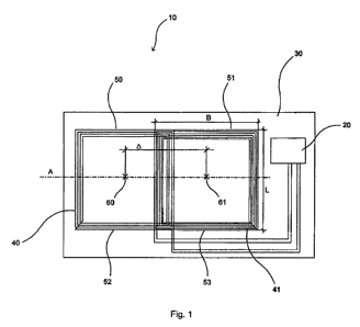
Figure 1 an embodiment of the RF component according to the invention;
Figure 2 an electronic display with an RF component according to Figure 1;
and
Figure 3 a representation of the coupling factor between two antenna coils as
a
function of the relative shift of the two antenna coils with respect to
each other.
Figure I shows an embodiment of the RF component according to the invention,
whereby an RF component (RF = radio frequency) as set forth in this invention
is
a component that has means to receive and process high-frequency radio
signals.
The term processing of radio signals means, among other things, the
acquisition of
energy from radio signals of a base station through induction and/or the
modula-
tion of an electromagnetic field of a base station.
The RF component 10 consists of at least of a non-conductive carrier 30 on
which
two antenna coils 40 and 41 and an electronic assembly such as, for example, a
microchip 20 with an integrated circuit, are arranged. The carrier is
preferably flat
and plate-shaped. However, it can also consist of a film. The two antenna
coils are
connected to the microchip which, in turn, can be connected to an electronic
device that is to be supplied with energy and data via the antennas. As an
alterna-
tive, however, any other models and connections are possible. For example,
each
antenna coil can be connected to a microchip, or else a first antenna coil is
con-
CA 02713644 2010-07-29
WO 2009/121464 PCT/EP2009/001675
8
nected to a microchip, while a second antenna is connected to discrete
structural
components.
Electronic devices that can be operated with the RF component according to the
invention include, for example, electronic displays or sensors. However, the
invention can also be used for any applications in which electronic
information
and energy have to be transmitted. Examples of these are data recorders,
medical
implants such as cochlea implants, retina implants, cardiac pacemakers and neu-
ronal stimulators. Moreover, wirelessly operated actuators such as, for
example,
passively operated locking units or pumps are possibilities. However, then if
the
microchip comprises, for example, a memory in which data can be stored and
retrieved by a reading device, the RF component can also be used as an autonom-
ous component in the form of an RFID tag on objects, persons or animals, or
positions.
However, the invention is especially suitable for operating a display 70 that
is
based on electronic ink and that is of the type shown in Figure 2 with a
display
above a carrier 30 with two antennas 40 and 41. The RF component is connected
to the display 70 and it receives variable data that comes from a base station
and
that is to be shown on a display. As an alternative, variable data is stored
in a
memory of the microchip 20 or in another memory of the electronic display 70
that is activated by signals of a base station and that is displayed by means
of the
bi-stable elements of the electronic ink. Energy is needed in order to
influence the
orientation of the bi-stable elements of the electronic ink, and this energy
is like-
wise received via the RF component 10.
The non-conductive carrier 30 preferably consists of a plastic. For example,
it is
possible to use fiberglass mats impregnated with epoxy resin, which are also
known for use in printed circuit boards. At least two conductive antenna coils
40
and 41 are printed onto the carrier 30 or created there using etching methods.
In
order to better differentiate between the two coils, the windings of a first
antenna
CA 02713644 2010-07-29
WO 2009/121464 PCT/EP2009/001675
9
coil 40 are depicted with a broken line in Figure 1, while the windings of a
second
antenna coil 41 are depicted with a solid line. In the embodiment shown in
Figure
1, these are four rectangular coils, each with at least one winding and
rounded-off
corners. However, any curved or polygonal shapes with at least one winding are
conceivable.
Preferably, an antenna coil has several windings and their ends are connected,
for
example, to the microchip 20, to additional microchips or to other discrete
com-
ponents. Furthermore, it is possible to provide more than two antennas on one
car-
rier 30. The coils have to be arranged in accordance with the antenna
arrangement
according to the invention so as to be shifted with respect to each other in
such a
way that their coupling is very slight or equal to zero. In the case of
several coils,
the arrangements needed for this purpose can be ascertained by analytical
expres-
sions, by simulation tools or by empirical determination.
According to the invention, the first antenna coil 40 is a high-quality,
narrow-band
energy coil. This coil serves to supply the microchip 20 and a connected
device
with energy in that a current flow is generated through induction as soon as
the
energy coil 40 enters the high-frequency electromagnetic field of a base
station. A
second antenna coil 41 is a lower-quality, broadband data coil. This antenna
coil
41 serves to transmit data to the microchip or to a connected electronic
device.
In accordance with the antenna arrangement according to the invention, the two
antennas are arranged in two different layers on the carrier 30 and they do
not
touch each other. Moreover, the antenna coils 40 and 41 are arranged so as to
be
offset with respect to each other on the surface of the carrier 30. The two
antennas
are positioned in such a way that the mutual inductance and thus the coupling
of
the two antenna coils are minimized or even equal to zero. If a current is
flowing
in one antenna, this has little or no effect on the other antenna. A current
flow, for
example, in the energy coil 40, causes a magnetic flux which, however, does
not
induce any voltage in the data coil and is completely decoupled, and vice
versa.
CA 02713644 2010-07-29
WO 2009/121464 PCT/EP2009/001675
The field lines run - in parts - in the direction of the normal vector and -
in other
parts - opposite thereto, so that the total flow adds up to zero.
Consequently, the
two antennas are decoupled from each other and can be operated completely sepa-
rately from each other.
5
The rectangular antenna coils 40 and 41 are preferably arranged in such a way
that
the windings of the energy coil 40 and the windings of the data coil 41
overlap in
a partial area of each individual antenna coil. In the embodiment shown in
Figure
I, the windings of the two coils overlap, for example, in the area of one
length-
10 wise side of a coil. In order to achieve this overlapping, the two antennas
are
advantageously applied in two different layers. The distance between these
layers
is preferably in the order of magnitude of 1 mm.
If the energy coil 40 and the data coil 41 - as is the case in the embodiment
in
Figure 1 - consist of one or more rectangular windings that are printed onto
the
carrier 30, then the two rectangular antenna coils thus formed have the same
orientation. The opposing sides 50 and 52 of a first antenna coil 40 thus run
parallel to the corresponding sides 51 and 53 of the second antenna coil 41.
In this
case, the antenna coils are arranged so as to be offset with respect to each
other
along an axis A that runs parallel to these four opposite sides 50, 51, 52 and
53 of
the two antenna coils 40 and 41. Here, the midpoints 60 and 61 of the two
antenna
coils undergo a relative shift A.
In the embodiment shown in Figure 1, both antennas 40 and 41 are equal in size
and have an outer length L = 50 mm and an outer width B = 50 mm. The first
coil
40 has four windings, whereas the second coil 41 has six windings. The
conductor
width of the first coil 40 is about I mm, while the conductor width of the
second
coil is about 0.75 mm. The distance between the conductors is about 0.3 min in
both antenna coils 40 and 41. The distance between the two layers of the
antenna
coils is in the order of magnitude of 0.1 min to 2 mm, and preferably at about
I
CA 02713644 2010-07-29
WO 2009/121464 PCT/EP2009/001675
it
min. However, any distances that are possible with the desired component can
be
realized.
In this case, it has been found that the two antennas have to be shifted
relative to
each other in such a way that their midpoints 60 and 61 have to be arranged so
as
to be offset with respect to each other by about A = 39 min along an axis A in
order to achieve a decoupling of the two antenna coils. In the case of other
coil
shapes and sizes, the requisite shifts are different and they will have to be
deter-
mined on a case-to-case basis. This can be done by means of tests and/or com-
puter simulations. A simulated coupling of the two described coils can be seen
in
the graph of Figure 3. Here, the requisite relative shift A in millimeters is
plotted
on the abscissa, whereas the coupling factor of the coils is plotted on the
ordinate.
The coupling factor is defined as the ratio between the mutual inductance and
the
square root of the product of the self-inductances. The coupling factor is
also
designated as k: k = MIL-,L, , wherein M is the mutual inductance of the two
coils with respect to each other and Ll and L2 are the self-inductances of the
coils.
As can be seen in Figure 3, a coupling factor of zero is obtained at a
relative shift
of the two antenna coils with respect to each other of approximately A = 39
mm,
so that the two antennas are decoupled in such an arrangement and can be oper-
ated independently of each other.
In an especially preferred embodiment of the invention, the energy coil 40 and
the
data coil 41 can be operated at the same frequency. This frequency is, for
exam-
ple, 13.56 MHz. This has the advantage that an appertaining base station does
not
need a multi-antenna system in order to provide energy and data, but rather
can be
operated at one frequency.
Figure 2 shows an electronic display 70 above an RF component 10 according to
the invention. The display 70, like the RF component 10, is preferably
configured
CA 02713644 2010-07-29
WO 20091121464 PCT/EP2009/001675
12
to be very flat so that said display 70 - when applied onto the RF component -
forms a flat electronic device that can be used, for example, as a label in
various
areas of application where variable information is to be shown on a display.
The
electronic display medium employed is preferably electronic ink, based on bi-
sta-
ble elements. Chemically speaking, these are microcapsules containing two
differ-
ent color components that have different charges and that are oriented in the
elec-
tric field. Due to the particle sizes and the viscosity of the system,
relaxation back
to the unordered initial state does not occur immediately after the electric
field has
been switched off. Hence, the written information is not lost but, at most,
there is
merely a decrease in the contrast.
Examples of electronic ink are the products SmartPaperTM made by the Gyricon
company and electrophoretic displays made by the E Ink company.
Electrophoretic displays have favorable properties, especially in terms of the
mechanical requirements regarding flexibility, impact-resistance and pressure-
stability, so that they are especially well-suited for use as labels.
Furthermore,
they have sufficient bi-stable behavior and the circuitry required for the
energy
supply is limited, thanks to the relatively low control voltage.
The energy received from a base station by the energy coil 40 serves to
operate
the microchip 20 and the electronic display 70. Moreover, a logic circuit can
be
integrated that performs data management and that transfers data from the data
coil 41 of the RF component 10 to the display. Texts as well as encrypted
infor-
mation, for example, in the form of barcodes, can be shown on the display in
that
the bi-stable elements of the electronic ink are oriented accordingly. The
informa-
tion is displayed until a base station activates the display of new
information,
whereby the energy needed one time for the new information display is obtained
via the energy coil 41.
CA 02713644 2010-07-29
WO 2009/121464 PCT/EP2009/001675
13
List of reference numerals
0 RF component
20 electronic assembly, microchip
30 carrier
40 antenna coil, energy coil
41 antenna coil, data coil
50,51,52,53 sides of the rectangle
60, 61 midpoint of an antenna coil
70 electronic display
L outer length of an antenna coil
B outer width of an antenna coil
A relative shift