Note: Descriptions are shown in the official language in which they were submitted.
CA 02713771 2013-05-08
HOLSTER-INTEGRATED PIEZOELECTRIC ENERGY SOURCE FOR HANDHELD
ELECTRONIC DEVICE
The present disclosure relates generally to energy sources for handheld
electronic
device. More particularly, the present disclosure relates to holster-
integrated energy
sources for handheld electronic devices.
Handheld electronic devices (HEDs) are typically equipped with a battery that
requires recharging at regular intervals in order for the HED to remain
functional.
Although advances in battery technology have provided longer time periods
between
recharging the batteries, recharging is still required and can be
inconvenient.
Some HEDs can include built-in piezoelectric energy sources; however the
integration of piezoelectric members and circuitry into an HED can increase
the
dimensions of the HED, which goes against the trend of miniaturization of such
devices.
Other approaches to using piezoelectric energy sources with HEDs include
having a
piezoelectric charge module that can be removably secured to an HED while the
HED is
not in use. This makes for a bulky HED/piezoelectric arrangement.
GENERAL
The following disclosure is generally directed to holster for a handheld
electronic
device, into which the HED can be inserted and withdrawn by a user. The
holster is
typically configured to retain the HED when the user inserts the HED into the
holster, and
is further configured to make the HED readily accessible for withdrawal by the
user. For
purposes of illustration, the HED is equipped with a rechargeable battery. The
holster
includes one or more piezoelectric elements that generate an input voltage,
and further
includes charging circuitry. The charging circuitry includes an electrical
connector that is
configured to electrically couple to the HED when the HED is inserted into the
holster. As
will be described below, the holster is configured to charge the rechargeable
battery of
the HED when the HED is inserted in the holster.
Generally, the present disclosure provides a holster for a HED, the holster
may
have integrated therein one or more piezoelectric elements and charging
circuitry that can
provide useful output voltage and current to the HED upon the HED being
inserted in the
holster to electrically connect the HED to the charging circuitry. The
electrical connection
may typically by way of a mating connector electrically couple the HED to the
charging
circuitry. The concepts described herein are not limited to any particular
kind of electrical
connection or connector, and can include, for example, tab-terminal-to-tab-
terminal
1
CA 02713771 2013-05-08
connections, plug-to-socket connections and spring-loaded-holster. Each
elongated
member can be substantially parallel to the cavity length. Each elongated
member can be
substantially perpendicular to the cavity length. The holster can define a
housing for
receiving the handheld electronic device, the holster can further comprise a
fastening
element secured to the housing, the fastening element being rotatable with
respect to the
housing to change an orientation of the housing with respect to the fastening
element.
The fastening element can includes a clip.
In a second aspect, the present disclosure may provide a system comprising a
holster with a handheld device.
In a third aspect, the present disclosure may provide a holster for a handheld
electronic device. The holster may comprise: at least one piezoelectric
element to
generate an input voltage upon being deformed; charging circuitry electrically
connected
to the at least one piezoelectric element; and a coil electrically connected
to the charging
circuitry. The charging circuitry may be to provide an output voltage to the
coil in
accordance with the input voltage and in accordance with pre-determined
charging circuit
parameters. The coil may be to inductively couple the charging circuitry to
the handheld
electronic device upon the handheld electronic device being inserted into the
holster. The
charging circuitry and the coil can define an assembly that has an assembly
resonant
frequency; and the at least one piezoelectric element can have a piezoelectric
element
resonant frequency. The assembly resonant frequency can be substantially equal
to the
piezoelectric element resonant frequency. The charging circuitry can comprise
at least
one capacitor.
It will be appreciated that for simplicity and clarity of illustration, where
considered
appropriate, reference numerals may be repeated among the figures to indicate
corresponding or analogous elements. In addition, numerous specific details
are set forth
in order to provide a thorough understanding of the embodiments described
herein.
However, it will be understood by those of ordinary skill in the art that the
embodiments
described herein may be practiced without these specific details. In other
instances, well-
known methods, procedures and components have not been described in detail so
as not
to obscure the embodiments described herein. Also, the description is not to
be
considered as limited to the scope of the embodiments described herein.
BRIEF DESCRIPTION OF THE DRAWINGS
Embodiments of the present disclosure will now be described, by way of example
only, with reference to the attached Figures, wherein:
2
CA 02713771 2013-05-08
Figure 1 shows a front view of an exemplary embodiment of the holster of
the present disclosure;
Figure 2 shows a side view of the holster of Figure 1;
Figure 3 shows a side cross-sectional view of the holster of Figure 1;
Figure 4 shows a front cross-sectional view of the holster of Figure 1;
Figure 5A shows a block diagram depiction of an exemplary charging
circuit;
Figure 5B shows another exemplary charging circuit;
Figure 5C shows yet another exemplary charging circuit;
Figure 6 shows a side cross-sectional view of another exemplary
embodiment of the present disclosure;
Figure 7 shows a front cross-sectional view of the holster of Figure 6;
Figure 8 shows an exemplary arrangement of interleaved piezoelectric
elements; and
Figure 9 shows block diagram representation of a handheld electronic
device that can be used with the holster of the present disclosure.
DESCRIPTION OF PREFERRED EMBODIMENTS
Figure 1 shows a front view of an exemplary embodiment of a holster 21 of the
present disclosure. Figure 2 shows a side view of the holster 21. The holster
21 can be
used for any suitable handheld electronic device (HED) that runs on
electricity, which is
typically provided by a battery or by any other suitable electrical charge
storage device
such as, for example, a capacitor. A flexible holster cover 22 is also shown
at Figs. 1
and 2, and serves to hold and secure the HED in the holster 21. The holster 21
can have
and exterior portion made of any suitable material (having any desirable
aesthetic,
electrical, durability, strength, or other characteristics or combinations of
characteristics)
such as, e.g., leather, nylon, etc. The holster cover 22 can be held closed
through any
suitable means such as, for example, a magnetic closure, a hook and loop
closer, a snap-
fit closure, etc. As will be understood by the skilled worker, holsters not
having a cover
are also within the scope of the present invention. A clip 80, shown at Figure
2, allows a
user to secure the holster 21 to a belt, purse, pocket etc. As will be further
be
understood by the skilled worker, any other suitable fastening element such
as, e.g., a
loop for connecting to a belt can be used. Additionally, the holster of the
present
disclosure can also function without any fastening element. When present, the
fastening
element, in the present example, the clip 80, can be rotatable with respect to
the housing
3
CA 02713771 2013-05-08
82 of the holster, and to the user to which it is fastened, to permit a change
in the
orientation of housing with respect to the user. This variable orientation of
the housing
can allow the user to set the orientation in order to adjust the amount of
vibration energy
being harvested.
Figure 3 shows a side cross-sectional view of the holster 21 taken along of
Figure 1. As shown at Figure 3, the holster 21 defines a cavity 33 along the
length of
which, the length direction being indicated by arrow 35, a HED can be slid in
and out of
the holster. Figure 3 also shows a chamber 24 that houses one or more
piezoelectric
element 26, each of which is fixedly secured at a first portion 27 to the
chamber 24 by a
holder 28, which can be any suitable type of clamp or holding device.
Alternatively, any
other suitable means to secure the first portion 27 to the chamber 24 can be
used such
as, e.g., adhesives, press-fits, snap fits, fasteners, etc. Each piezoelectric
element 26
has a second portion 29, which movable with respect to the first portion 27
and to the
chamber 24, upon the holster being accelerated in any suitable direction. As
shown at
Figure 3, and at Figure 4 described below, the piezoelectric element 26 is
substantially
parallel to the length of the cavity 33.
Figure 4 shows a front cross-sectional view of the holster 21 taken along line
IV-
IV of Figure 3. As shown at Figure 4, four piezoelectric elements 26 are
contained in the
chamber 24. However, any suitable number of piezoelectric elements 26 can be
used,
including one piezoelectric element 26, without departing from the scope of
the present
disclosure. If more than one piezoelectric elements 26 are present, they can
be
electrically connected to each other in parallel or in series, or in any
suitable
parallel/series configuration. The exemplary piezoelectric elements 26 are
rectangular-
shaped plates; however, this need not the case. Any suitably-shape
piezoelectric
elements can be used without departing from the scope of the present
disclosure. For
example, amongst others, disc-shaped, tube-shaped, and ring-shaped
piezoelectric
elements can also be used. The piezoelectric elements 26 can have any suitable
dimensions. For example, the thickness can range from less than a tenth of a
millimeter
to several millimeters; and, the length and width can range from one to
several
millimeters. As will be understood by the skilled worker, the dimensions of
the
piezoelectric elements can be determined in accordance with, amongst other
factors: (a)
the choice of the piezoelectric material of the piezoelectric elements 26; (b)
the required
voltage/current characteristics of the HED; and (c) the principal frequencies
to which the
holster 21 is subjected during the activity practiced by the user, at which
energy
harvesting is achieved. The concepts described herein are not necessarily
limited to any
4
CA 02713771 2013-05-08
particular number of piezoelectric elements 26, or to any particular
electrical connection of
piezoelectric elements, or to any particular shape or dimension of
piezoelectric elements,
or to any combination thereof.
As will be understood by the skilled worker, piezoelectric materials can
generate a
voltage upon being subjected to deformation, such deformations including, for
example,
bending, twisting, compression, elongation, etc. The piezoelectric elements 26
are
fabricated to undergo such deformations upon the holster being subjected to
accelerations such as those encountered when the holster is with a person
walking or
otherwise moving about. Such deformations will also typically occur when the
user is
travelling, e.g., on a plane or car; or when the holster 21 sits atop a
vibrating object such
as a refrigerator or an air conditioning unit.
Upon the holster 21 being subjected to an acceleration, the portion of the
piezoelectric element 26 that is not fixedly secured in the holder 28 (the
first portion 27),
can move with respect to the portion held in the holder 28. The resulting
deformation of
the piezoelectric element 26 generates a voltage at surfaces of the
piezoelectric material
comprised in the piezoelectric element 26. A double-arrowed arc 31 at Figure 3
shows
an exemplary movement that the second portion 29 can undergo upon the
piezoelectric
member 26 being accelerated.
Each piezoelectric element 26 is electrically connected to charging circuitry
32
disposed at the bottom region of the holster 21, as shown at Figs. 3 and 4.
Alternatively,
the charging circuitry 32 can be located at any other suitable region of the
holster 21
without departing from the scope of the present disclosure. In some cases,
charging
circuitry could be integrated in the HED itself without departing from the
scope of the
present disclosure. The connection of each piezoelectric element 26 to the
charging
circuitry is typically done though a pair of conductors (not shown), with a
first conductor
connecting the charging circuitry 32 to a first surface of the piezoelectric
material of the
piezoelectric element 26, and a second conductor connecting the charging
circuitry 32 to
a second surface of the piezoelectric material of the piezoelectric element
26. The
above-noted first and second surfaces of the piezoelectric material can be any
surfaces
across which a voltage is generated upon the piezoelectric element 26, and the
piezoelectric material itself, being deformed. The connection of the surfaces
in question to
their respective conductor can be achieved through any suitable electrode,
defining any
suitable pattern, formed on the surfaces.
The deformation of the piezoelectric elements 26 generates an input voltage
that
is provided to the charging circuitry 32. The charging circuitry 32 has an
electrical transfer
CA 02713771 2013-05-08
means, for example an electrical connector 30, that connects to the HED upon
the HED
being inserted in the holster 21. Any suitable type of electrical connector
can be used,
such as, for example, a mini-USB connector, provided the HED includes a
complementary connector to mate therewith. The charging circuitry 32 provides
an output
voltage to the HED in accordance with the input voltage and with pre-
determined charging
circuit parameters. As used herein, two elements are "in accordance with" one
another
when the value of one element corresponds to the value of another. For
example, two
elements may be 'in accordance with" one another when one is a function of the
other, or
when both vary in response to common factor. A charging circuit parameter is
"pre-
determined" in the sense that at least one aspect of the parameter is defined
prior to
charging. Such charging circuit parameters can include, for example, target
output
voltage and target output current. Any suitable type of charging circuitry can
be used.
The inputs to the design can include many factors such as, for example, input
frequency,
resonant frequency, frequency ranges, output voltage and currents etc., and
the tradeoffs
between these factors. Examples of such circuitry can be found in, amongst
other
references, the article by Y.-P. Liu et al. entitled Velocity-Controlled
Piezoelectric
Switching Energy Harvesting Device, proceedings of International Conference on
Renewable Energy and Power Quality, Valencia, Spain, 15-17 April 2009.
Alternatively, the charging circuitry and the HED can include as an electrical
transfer means inductive charging circuitry components to allow inductive
charging of the
HED by the piezoelectric elements. In such cases, as will be understood by the
skilled
worker, the connector 30 is not required. Rather, as will be described below,
an induction
coil can be used instead.
Figure 5A shows a block diagram of an exemplary charging circuitry 32
electrically connected to the piezoelectric members 26. The charging circuitry
32 can
include, as shown in the present exemplary embodiment, a rectifier module 42,
a
capacitor assembly 44 and discharge circuitry 46. The piezoelectric members 26
provide
a time-varying input voltage (this voltage being output from the piezoelectric
members 26
but being input to the charging circuitry 32) that is input into the rectifier
module 42. In
turn, the rectifier module 42 provides a rectified voltage to the capacitor
assembly 42,
which can include one or more capacitors that are charged by the rectified
voltage. The
capacitor assembly 42 stores at least some of the energy harvested from the
piezoelectric members 26. This storage of energy can occur whether the HED is
inserted
in the holster or not. The discharge circuitry 46, in accordance with pre-
determined
parameters, causes the capacitors of the capacitor assembly 44 to discharge
and
6
CA 02713771 2013-05-08
provides an output voltage to an HED electrically connected to the connector
30. This
output voltage is fed to a voltage regulator of the HED and can serve to power
the HED
while inserted in the holster 21, to charge the battery of the HED, or both.
The output
voltage provided to the electrical connector 30 is in accordance with the
input voltage
generated by the piezoelectric members 26 in that the output voltage is a
function of the
input voltage. The connector 30 can be referred to as a coupling element that
electrically
connects the charging circuitry 32 to the HED. Alternatively, the connector 30
can also be
referred to as an electrical transfer means that electrically connects the
charging circuitry
32 to the HED.
Figure 5B shows an exemplary charging circuitry having a full wave rectifier
106
electrically connected to a piezoelectric member 26 through connectors 102 and
104. A
capacitor 108 and a resistor 110, connected in parallel to the rectifier 106
provide and
output voltage to a HED (not shown).
Figure 5C shows a block diagram of another exemplary charging circuitry 150
used to magnetically couple energy harvested by the piezoelectic members 26 to
the
HED. The charging circuitry 150 is electrically connected to the piezoelectric
members
26, which act as an AC source. The charging circuitry 150 can include
capacitors, shown
as capacitor circuitry 160, electrically connected to a charge coil 152, which
is typically
made of an electrically conductive material. As will be understood by the
skilled worker, a
magnetic core can be placed adjacent the charge coil 152 to vary the degree of
magnetic
coupling to the HED. The characteristics of the charge coil 152 and of the
charging
circuitry 150 can be chosen such that the assembly formed by the charge coil
152 and
the charging circuitry 150 has a resonance frequency substantially equal to
that of the
piezoelectric members 26. As will be understood by the skilled worker, a HED
to be
charged by the piezoelectric members/charging circuitry/coil assembly shown in
the
example of Figure 5C, needs to include its own magnetic inductive coupling
assembly,
which can include, for example, a coil and a magnetic core, operatively
connected to
battery of the HED. The charge coil 152 can be referred to simply as a coil or
as a
magnetic induction coupling element that inductively couples the charging
circuitry 150 to
the HED upon the HED being inserted into the holster. The charge coil 152 can
also be
referred to as a near filed charge coil. Alternatively, the charge coil 152
can be referred to
as an electrical transfer means that is electrically connected to the charging
circuitry 152.
The charge coil can have any suitable shape such as, for example square,
round,
elliptical shapes, and include any number of turns.
The holster of present disclosure can itself include a rechargeable battery
that can
7
CA 02713771 2013-05-08
be recharged upon the holster, and its piezoelectric elements, being subjected
to
vibrations. In such embodiments, the HED recharges its own battery from the
holster's
battery upon the HED being inserted into the holster. As such, a user carrying
the holster
will recharge the holster's battery even when the HED is out of the holster.
The piezoelectric element 26 can include a laminar arrangement of a substrate
and one or more piezoelectric layers. The substrate can be made of any
suitable material
such as, e.g., aluminum, steel, silicon nitride, etc., and the piezoelectric
material can
include any suitable material such as, e.g., lead zirconate titanate (PZT).
The
piezoelectric material can be formed on the substrate by slurry deposition or
by any other
suitable methods. Alternatively, the piezoelectric element 26 can be produced
without a
substrate. The piezoelectric element 26 can include a plurality of
piezoelectric layers.
Each of these piezoelectric layers can be substantially similar to the others,
therefore
having similar mechanical and electrical properties. Alternatively, each layer
can be
different from some of the others in terms of, for example, composition, and
thickness,
therefore having different mechanical and electrical properties. In such a
case, a first
piezoelectric layer could have a frequency response different than that of
another different
piezoelectric layer, allowing for the harvest of vibration energy at different
frequencies.
Although the piezoelectric elements 26 of the embodiment of the holster 21 are
elongated members fixedly secured to chamber 24 at their first end 27 in a
cantilever
arrangement, any other suitable arrangement and shape of piezoelectric
elements can be
used without departing from the scope of the present disclosure. For example,
elongated
piezoelectric beams fixedly secured to the chamber 24 at their opposite ends,
with their
mid-sections undergoing movement, and deformation, upon the holster being
accelerated, are also within the scope of the present disclosure. As a further
example,
disc-shaped piezoelectric elements having their perimeter portion secured to
the chamber
24 and their centre portion moving undergoing movement, and deformation, upon
the
holster being accelerated, are also within the scope of the present
disclosure.
Additionally, as will be understood by the skilled worker, the piezoelectric
voltage
characteristics can be adjusted by fixing a weight to a portion of the
piezoelectric element
undergoing movement without departing from the scope of the present
disclosure.
Figure 6 shows a side cross-sectional view of another exemplary embodiment of
a holster 50 of the present disclosure. Figure 7 shows a front cross-sectional
view of the
holster 50 taken along the line VII-VII of Figure 6. In the holster 50, the
piezoelectric
elements 26 are contained in a chamber 24 at the bottom region of the holster
50. The
charging circuit 32 is also formed at the bottom region of the holster 50. As
in the holster
8
CA 02713771 2013-05-08
21 described above, the charging circuitry 32 includes a connector 30 that
connects to a
HDE upon the HED being inserted in the holster 50. As in the holster 21, the
holster 50
also defines a cavity 33 along the length of which (arrow 35) a HED can be
slid in and
out. In the holster 50 the piezoelectric members 26 are substantially
perpendicular to the
length of the holster, the direction of the length being indicated by the
arrow As will be
understood by the skilled worker, holsters with an open, or partly open, wall
are also
within the scope of the present disclosure.
As will be understood by the skilled worker, a holster with multiple groups of
piezoelectric elements disposed in corresponding multiple compartment is also
within the
scope of the present disclosure. For example, although not shown, a holster
having a
first group of piezoelectric elements oriented along the insertion direction
of a HED, that
is, a direction such as direction 35 at Figures 3 and 6, and having a second
group of
piezoelectric elements oriented perpendicularly to the first group of
piezoelectric
elements, is within the scope of the present disclosure. The first and second
groups of
piezoelectric elements could also be disposed in a same compartment without
departing
from the scope of the present invention.
Figure 8 shows an exemplary embodiment of an arrangement 60 of piezoelectric
elements 26 that can be integrated into a holster. The arrangement 60 includes
a first
comb 62 of piezoelectric elements, and a second comb 64 of piezoelectric
elements. The
first and second combs 62 and 64 are interleaved and, although not shown, can
be
electrically connected to any suitable charging circuitry such as charging
circuitry 32
described above. As will be understood by the skilled worker, the arrangement
60 can
provide enhanced voltage while maintaining relatively small dimensions of the
compartment in which they are housed.
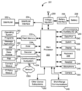
Referring Figure 9, there is shown therein a block diagram of an exemplary
embodiment of a HED 201 that can be combined with the holster of the present
disclosure, exemplified in embodiment 21 and 50 above.
The HED 201 includes a number of components such as the processor 222 that
controls the overall operation of the HED 201. Communication functions,
including data
and voice communications, are performed through a communication subsystem 224.
Data received by the HED 201 can be decompressed and decrypted by a decoder
226,
operating according to any suitable decompression techniques (e.g. YK
decompression,
and other known techniques) and encryption techniques (e.g. using an
encryption
technique such as Data Encryption Standard (DES), Triple DES, or Advanced
Encryption
Standard (AES)). The communication subsystem 224 receives messages from and
sends
9
CA 02713771 2013-05-08
messages to a wireless network 1000. In this exemplary embodiment of the HED
201, the
communication subsystem 224 is configured in accordance with the Global System
for
Mobile Communication (GSM) and General Packet Radio Services (GPRS) standards.
The GSM/GPRS wireless network is currently used worldwide. New standards such
as
Enhanced Data GSM Environment (EDGE) and Universal Mobile Telecommunications
Service (UMTS) & LTE are believed to have similarities to the network behavior
described
herein, and it will also be understood by persons skilled in the art that the
embodiments
described herein are intended to use any other suitable standards that are
developed in
the future. The wireless link connecting the communication subsystem 224 with
the
wireless network 1000 represents one or more different Radio Frequency (RF)
channels,
operating according to defined protocols specified for GSM/GPRS
communications. With
newer network protocols, these channels are capable of supporting both circuit
switched
voice communications and packet switched data communications.
Although the wireless network 1000 associated with the HED 201 is a GSM/GPRS
wireless network in one exemplary implementation, other wireless networks may
also be
associated with the HED 201 in variant implementations. The different types of
wireless
networks that may be employed include, for example, data-centric wireless
networks,
voice-centric wireless networks, and dual-mode networks that can support both
voice and
data communications over the same physical base stations. Combined dual-mode
networks include, but are not limited to, Code Division Multiple Access (CDMA)
or
CDMA1000 networks, GSM/GPRS networks (as mentioned above), and future third-
generation (3G) networks like EDGE and UMTS. Some other examples of data-
centric
networks include WiFi 802.11, Mobitex TM and DataTACTm WiMax network
communication
systems. Examples of other voice-centric data networks include Personal
Communication
Systems (PCS) networks like GSM and Time Division Multiple Access (TDMA)
systems.
The processor 222 also interacts with additional subsystems such as a Random
Access Memory (RAM) 228, a flash memory 230, a display 232, a keyboard 238, a
switch
239, an auxiliary input/output (I/0) subsystem 240, a data port 242, a speaker
244, a
microphone 246, short-range communications 248, a camera 300, and other device
subsystems 250.
Some of the subsystems of the HED 201 perform communication-related
functions, whereas other subsystems may provide "resident" or on-device
functions. By
way of example, the keyboard 238 may be used for both communication-related
functions, such as entering a text message for transmission over the network
1000, and
device-resident functions such as a calculator or task list.
CA 02713771 2013-05-08
The HED 201 can send and receive communication signals over the wireless
network 1000 after network registration or activation procedures have been
completed.
Network access is associated with a subscriber or user of the HED 201. To
identify a
subscriber according to the present embodiment, the HED 201 uses a SIM/RUIM
card
252 (i.e. Subscriber Identity Module or a Removable User Identity Module)
inserted into a
SIM/RUIM interface 254 for communication with a network such as the network
1000. The
SIM/RUIM card 252 is one type of a conventional "smart card" that can be used
to identify
a subscriber of the HED 201 and to personalize the HED 201, among other
things. In the
present embodiment the HED 201 is not fully operational for communication with
the
wireless network 1000 without the SIM/RUIM card 252. By inserting the SIM/RUIM
card
252 into the SIM/RUIM interface 254, a subscriber can access all subscribed
services.
Services may include: web browsing and messaging such as e-mail, voice mail,
Short
Message Service (SMS), and Multimedia Messaging Services (MMS). More advanced
services may include: point of sale, field service and sales force automation.
The
SIM/RUIM card 252 includes a processor and memory for storing information.
Once the
SIM/RUIM card 252 is inserted into the SIM/RUIM interface 254, it is coupled
to the
processor 222. In order to identify the subscriber, the SIM/RUIM card 252 can
include
some user parameters such as an International Mobile Subscriber Identity
(IMSI). An
advantage of using the SIM/RUIM card 252 is that a subscriber is not
necessarily bound
by any single physical mobile electronic device. The SIM/RUIM card 252 may
store
additional subscriber information for a HED as well, including datebook (or
calendar)
information and recent call information. Alternatively, user identification
information can
also be programmed into the flash memory 230. The HED 201 can also be enabled
to
receive additional memory cards. For example, memory card slots (not shown)
can be
provided in the HED 201 to receive such cards.
The HED 201 is a battery-powered device and includes a battery interface 256
for
receiving a battery pack containing one or more rechargeable battery cells
258, and
associated control circuitry (not shown) that, in some embodiments, can
interface with the
battery interface 256. The battery pack has a form factor and contact
arrangement suited
to the particular handheld electronic device. In at least some embodiments,
the battery
258 can be a smart battery with an embedded microprocessor. The battery
interface 256
is coupled to a voltage regulator 259, which assists the battery 258 in
providing voltage
V+ to the HED 201. Additionally, the voltage regulator 259 connects, through
an HED
connector formed in at the HED 201, to the connector 30 shown, e.g., at Figure
3, to
receive a voltage from the discharge circuitry 46 of the charging circuitry 32
exemplified at
11
CA 02713771 2013-05-08
Figure 5. As described below, the HED connector can be a data port 242.
Although
current technology makes use of a battery, alternatives to batteries, such as
capacitors, or
future technologies such as micro fuel cells may provide the power to the HED
201. The
concepts described herein are not necessarily limited to any particular kind
of battery, or
to any particular battery chemistry, or to batteries that use energy storage
elements or
techniques other than or in addition to chemical energy storage. On the
contrary, the
concepts described herein may be applicable to a variety of chargeable or
rechargeable
power packs, including those that are distinct from conventional batteries.
The HED 201 also includes an operating system 260 and software components
262 which are described in more detail below. The operating system 260 and the
software
components 262 that are executed by the processor 222 are typically stored in
a
persistent store such as the flash memory 230, which may alternatively be a
read-only
memory (ROM) or similar storage element (not shown). Those skilled in the art
will
appreciate that portions of the operating system 260 and the software
components 262,
such as specific software applications 264, 266, 268, 270 and 272, or parts
thereof, may
be temporarily loaded into a volatile store such as the RAM 228. Other
software
components can also be included, as is well known to those skilled in the art.
The subset of software components 262 that control basic device operations,
including data and voice communication applications, will normally be
installed on the
HED 201 during its manufacture. Other software applications include a message
application 264 that can be any suitable software program that allows a user
of the HED
201 to send and receive electronic messages. Various alternatives exist for
the message
application 264 as is well known to those skilled in the art. Messages that
have been sent
or received by the user are typically stored in the flash memory 230 of the
HED 201 or
some other suitable storage element in the HED 201. In at least some
embodiments,
some of the sent and received messages may be stored remotely from the HED 201
such
as in a data store of an associated host system that the HED 201 communicates
with.
The software components 262 can further include a device state module 266, a
Personal
Information Manager (PIM) 268, and other suitable modules (not shown). The
device
state module 266 provides persistence, i.e. the device state module 266
ensures that
important device data is stored in persistent memory, such as the flash memory
230, so
that the data is not lost when the HED 201 is turned off or loses power.
The PIM 268 includes functionality for organizing and managing data items of
interest to the user, such as, but not limited to, e-mail, contacts, calendar
events, voice
mails, appointments, and task items. The PIM 268 has the ability to send and
receive
12
CA 02713771 2013-05-08
data items via the wireless network 1000. PIM data items may be seamlessly
integrated,
synchronized, and updated via the wireless network 1000 with the HED
subscriber's
corresponding data items stored or associated, or both, with a host computer
system.
This functionality creates a mirrored host computer on the HED 201 with
respect to such
items. This can be particularly advantageous when the host computer system is
the HED
subscriber's office computer system.
The software components 262 also include a connect module 270, and an
information technology (IT) policy module 272. The connect module 270
implements the
communication protocols that are required for the HED 201 to communicate with
the
wireless infrastructure and any host system, such as an enterprise system,
that the HED
201 is authorized to interface with.
The connect module 270 includes a set of APIs that can be integrated with the
HED 201 to allow the HED 201 to use any number of services associated with the
enterprise system. The connect module 270 allows the HED 201 to establish an
end-to-
end secure, authenticated communication pipe with the host system. A subset of
applications for which access is provided by the connect module 270 can be
used to pass
IT policy commands from the host system to the HED 201. This can be done in a
wireless
or wired manner. These instructions can then be passed to the IT policy module
272 to
modify the configuration of the HED 201. Alternatively, in some cases, the IT
policy
update can also be done over a wired connection.
Other types of software applications can also be installed on the HED 201.
These
software applications can be third party applications, which are added after
the
manufacture of the HED 201. Examples of third party applications include
games,
calculators, utilities, etc.
The additional applications can be loaded onto the HED 201 through at least
one
of the wireless network 1000, the auxiliary I/0 subsystem 240, the data port
242, the
short-range communications subsystem 248, or any other suitable device
subsystem 250.
This flexibility in application installation increases the functionality of
the HED 201 and
may provide enhanced on-device functions, communication-related functions, or
both. For
example, secure communication applications may enable electronic commerce
functions
and other such financial transactions to be performed using the HED 201.
The data port 242 enables a subscriber to set preferences through an external
device or software application and extends the capabilities of the HED 201 by
providing
for information or software downloads to the HED 201 other than through a
wireless
communication network. The alternate download path may, for example, be used
to load
13
CA 02713771 2013-05-08
an encryption key onto the HED 201 through a direct and thus reliable and
trusted
connection to provide secure device communication.
The data port 242 can be any suitable port that enables data communication
between the HED 201 and another computing device. The data port 242 can be a
serial
or a parallel port. In some instances, the data port 242 can be a USB port
that includes
data lines for data transfer and a supply line that can provide a charging
current to charge
the battery 258 of the HED 201.
The short-range communications subsystem 248 provides for communication
between the HED 201 and different systems or devices, without the use of the
wireless
network 1000. For example, the short-range communications subsystem 248 may
include
an infrared device and associated circuits and components for short-range
communication. Examples of short-range communication standards include
standards
developed by the Infrared Data Association (IrDA), Bluetooth, and the 802.11
family of
standards developed by IEEE.
Synchronization of files and data between the HED 201 and another computing
device can be achieved over the wireless network 1000, through the short-range
communications system 248, or through a direct connection between the data
port 242 of
the HED 201 and the other computing device. Synchronization causes the most
recent
version of files and data to be mirrored on either the HED or the other
computing device.
As used herein, synchronization also refers to the downloading or uploading of
pre-
selected files from one device to the other. Synchronization of files and data
can be
initiated by the user of the device whenever a suitable connection between the
HED 201
and another computing device, such as a home computer, is detected, or can
occur
automatically when a connection is detected. A synchronization application,
stored in the
HED 201 or the other computing device, or both, can determine the file and
data types to
be synchronized, the frequency of synchronization, and other parameters,
appropriate to
the particular synchronization algorithm implemented by the synchronization
application.
In use, a received signal such as a text message, an e-mail message, or web
page
download is processed by the communication subsystem 224 and input to the
processor
222. The processor 222 then processes the received signal for output to the
display 232
or alternatively to the auxiliary I/0 subsystem 240. A subscriber may also
compose data
items, such as e-mail messages, for example, using the keyboard 238, and,
possibly, the
auxiliary I/0 subsystem 240. The auxiliary I/0 subsystem 240 may include
devices such
as: a mouse, track ball, infrared fingerprint detector, or a roller wheel with
dynamic button
pressing capability. A composed item may be transmitted over the wireless
network 1000
14
CA 02713771 2013-05-08
through the communication subsystem 224.
For voice communications, the overall operation of the HED 201 is
substantially
similar, except that the received signals are output to the speaker 244, and
signals for
transmission are generated by the microphone 246. Alternative voice or audio
I/0
subsystems, such as a voice message recording subsystem, can also be
implemented on
the HED 201. Although voice or audio signal output is accomplished primarily
through the
speaker 244, the display 232 can also be used to provide additional
information such as
the identity of a calling party, duration of a voice call, or other voice call
related
information.
In the preceding description, for purposes of explanation, numerous details
are set
forth in order to provide a thorough understanding of the embodiments of the
disclosure.
However, it will be apparent to one skilled in the art that these specific
details are not
required in order to practice the disclosure. In other instances, well-known
electrical
structures and circuits are shown in block diagram form in order not to
obscure the
disclosure. For example, specific details are not provided as to whether the
embodiments
of the disclosure described herein are implemented as a software routine,
hardware
circuit, firmware, or a combination thereof.
The concepts described above may realize one or more advantages. Recharging
of a battery in an HED can be very convenient for a user, as the recharging
can take
place automatically when the user inserts the HED into the holster. The user
need not
even be aware that recharging is occurring. Further, because the holster may
be secured
to the user (such as at the user's pocket or belt), the holster may be in
motion as the user
is in motion, and the piezoelectric elements may generate energy, which can be
stored
for recharging, even if the HED itself is stationary. The holster can harvest
energy
whether the HED is inserted in the holster or not. Some embodiments described
above
do not significantly add to the dimensions, bulk or weight of the HED. To the
extent that
there is any addition to the dimensions, bulk or weight of the holster, this
addition is less
likely to be noticed by or be an inconvenience to the user. A further
potential benefit is
that the holster can perform at least two functions at the same time:
retaining the HED for
access by the user, and coupling the piezoelectric charging circuitry to the
HED when the
HED is not in use. In some embodiments, inductive electrical coupling between
the HED
and the holster may enhance the convenience to the user by omitting a need for
a wired
electrical coupling between the HED and the holster.
The above-described embodiments of the disclosure are intended to be examples
only. Alterations, modifications and variations can be effected to the
particular
CA 02713771 2013-05-08
embodiments by those of skill in the art without departing from the scope of
the
disclosure, which is defined solely by the claims appended hereto.
16