Note: Descriptions are shown in the official language in which they were submitted.
CA 02714005 2010-08-04
WO 2009/099619 PCT/US2009/000728
ARRAY AND CANTILEVER ARRAY LEVELING
RELATED APPLICATIONS
This application claims priority to US provisional application serial no.
61/026,196
filed February 5, 2008 to Haaheim et al., which is hereby incorporated by
reference in its
entirety.
BACKGROUND
Sharp tips and nanoscale tips can be used for high resolution patterning,
wherein an
ink or patterning compound can be transferred from the tip to a solid surface.
For example,
the tip can be an atomic force microscope (AFM) tip attached to one end of a
cantilever or a
larger support structure. This direct write nanolithographic approach can
provide advantages
which competing nanolithographies may not provide including high registration
and
reasonable costs. The cantilever can be used in several embodiments including
for example:
(i) a single tip or cantilever, (ii) a linear array of tips or cantilevers,
and (iii) a two-
dimensional array of tips or cantilevers, e.g, multiple rows of linear arrays
of tips or
cantilevers. See, for example, Mirkin et al, WO 00/41213, WO 01/91855, Small,
2005, 10,
940-945; See also US Patent Nos. 7,005,378; 7,034,854; 7,060,977; 7,098,056;
and
7,102,656; to Nanolnk.
A need exists to improve these and related devices and methods. In particular,
for
example, a need exists for improvements which can be made to these methods,
instruments,
and devices, particularly as the tip density increases, cantilever embodiments
become
increasingly complex in a two-dimensional system, and as the processes are
adapted to be
commercial processes. For example, as the cantilever arrays become more
geometrically
complex and larger with more cantilevers, leveling of the array becomes more
difficult. For
example, if the method is not done properly, one tip may touch the surface
before another
second tip touches the surface, or the second tip may not even touch the
surface. Or it may
be difficult to know when the tips touch the surface. In many cases, it is
desired that most or
all of the tips are touching when writing, and most or all are off the surface
when not writing.
Once the two dimensional spatial profile of the array is established, it is
desirable to have a
high degree of planarity for the 2D array of tips or cantilever tips;
otherwise, during
lithography cantilevers and tips can be damaged or writing may not occur at
all. In particular,
a need exists to provide a leveling means that is efficient and accurate. In
some
1
CA 02714005 2010-08-04
WO 2009/099619 PCT/US2009/000728
embodiments, a need exists to improve systems wherein the array may have a
plurality of tips
but the array does not employ cantilevers.
SUMMARY
Embodiments provided herein include, for example, instruments and devices,
software, and methods of making and using the same.
For example, one embodiment is a method comprising: (i) providing at least one
array of cantilevers supported by at least one support structure, (ii)
providing at least one
substrate, (iii) providing at least one instrument to control the position of
the array with
respect to the substrate, (iv) leveling the array with respect to the
substrate, wherein the
leveling is performed via a user interface on the instrument which is adapted
to have the user
input positional information from the motors and piezoelectric actuator when
at least one
cantilever deflects from the substrate.
One embodiment is a method comprising: (i) providing at least one array of
cantilevers supported by at least one support structure, (ii) providing at
least one substrate,
(iii) providing at least one instrument to control the position of the array
with respect to the
substrate, (iv) leveling the array with respect to the substrate, wherein the
leveling is
performed via a user interface on the instrument which is adapted to have the
user input
positional information from the motors and piezoelectric extender when at
least one
cantilever deflects from the substrate.
Another embodiment is a method comprising: providing at least one array of
cantilevers supported by at least one support structure comprising at least
one viewport,
providing at least one substrate, providing at least one instrument to control
the position of
the array with respect to the substrate, leveling the array with respect to
the substrate,
wherein the leveling is performed with the instrument comprising software
further
comprising a user interface adapted to provide operational control and
iterative
measurements of differences between the relative positions of the viewports
with respect to
the substrate.
Another embodiment provides a method comprising: providing at least one array
of
cantilevers, providing at least one substrate, providing at least one
instrument to control the
position of the array, leveling the array with respect to the substrate,
wherein the instrument
comprises at least one piezoelectric extender and at least three motors,
wherein the
piezoelectric extender and the motors are adapted to provide the leveling of
the array.
2
CA 02714005 2010-08-04
WO 2009/099619 PCT/US2009/000728
Another embodiment provides a method comprising: providing at least one array
of
cantilevers comprising cantilever tips, providing at least one substrate,
wherein the position
of the array of cantilever tips with respect to the substrate is controlled by
at least one z-
piezoelectric extender and at least three z-axis motors in a triangular,
surrounding
relationship with respect to the array, wherein the z-axis motors are adapted
to raise and
lower the cantilever tips with respect to the substrate, adjusting the z-axis
motors until all the
cantilever tips are substantially level with respect to the substrate to an
unaided eye,
positioning the array so that the cantilevers deflect by a non-negligible
amount while fully
extending the z-piezoelectric extender, adjusting the z-piezoelectric extender
to determine
the relative position of the z-axis motors, and recording the positions for
future calibration
reference so that the method needs to be performed once.
Another embodiment provides a method comprising: providing at least one
surface
with topographical features, providing at least one substrate, providing at
least one
instrument to control the position of the features, leveling the array with
respect to the
substrate, wherein the instrument is adapted to provide leveling of the
surface by a software
routine adapted to provide iterative measurements of the positions of the
array.
Another embodiment provides a method of leveling comprising: providing at
least
one surface with topographical features, providing at least one substrate,
providing at least
one instrument to control the spatial position of the array, leveling the
array with respect to
the substrate, wherein the instrument comprises at least one piezoelectric
extender and at
least three motors adapted to provide the leveling of the array.
Another embodiment provides a method comprising: providing at least one
surface
with topographical features, providing a substrate, wherein the position of
the features with
respect to the substrate is controlled by at least one piezoelectric extender
and at least three
motors in a triangular, surrounding relationship with respect to the surface,
wherein the
motors are adapted to raise and lower the features with respect to the
substrate, adjusting the
motors until all the features are substantially level with respect to the
substrate to an unaided
eye, positioning the array so that the surface features touch the substrate by
a non negligible
amount, adjusting the piezoelectric extender to determine the relative
position of the motors,
and recording the positions for future calibration references so that the
method needs to be
performed once.
Another embodiment provides a software routine comprising a user interface,
wherein
the routine prompts a user to perform measurements and input measurement
results via the
interface, the routine performs calculations based on the results and controls
and monitors at
3
CA 02714005 2010-08-04
WO 2009/099619 PCT/US2009/000728
least one piezoelectric extender and at least three motors to provide leveling
of a device with
respect of a substrate.
Another embodiment provides a software routine comprising a user interface,
wherein
the routine can be adapted to perform automated measurements and iterative
calculations
and controls and monitors at least one piezoelectric extender and at least
three motors to
provide leveling of a device with respect of a substrate.
Another embodiment provides a method comprising: providing at least one array
of
cantilevers supported by at least one support structure, providing at least
one substrate,
providing at least one instrument comprising motors to control the position of
the array with
respect to the substrate, leveling the array with respect to the substrate,
wherein the leveling
step is carried out via a user interface on the instrument which is adapted to
have the user
input positional information for the motors when at least one cantilever
deflects from the
substrate.
Another embodiment is a method comprising: (i) providing at least one array of
tips,
(ii) providing at least one substrate, (iii) providing at least one instrument
to control the
position of the array of tips with respect to the substrate, (iv) leveling the
array with respect to
the substrate, wherein the leveling is performed via a user interface on the
instrument which
is adapted to have the user input positional information from the motors and
piezoelectric
actuator when at least one tip contacts the substrate. The tips can be
nanoscopic tips,
scanning probe microscope tips, polymer tips, or atomic force microscope tips.
Another embodiment provides a method comprising: providing at least one array
of
nanoscopic tips supported by at least one support structure, providing at
least one substrate,
providing at least three points of reference in X-Y plane with respect to the
substrate to
determine points of contact between tips and substrate, providing at least one
instrument
comprising motors and a piezoelectric extender to control the position of the
array with
respect to the substrate, leveling the array with respect to the substrate,
wherein the leveling
is carried out via a user interface on the instrument which is adapted to have
a user input
positional information from the motors and piezoelectric extender when at
least one
nanoscopic tip contacts the surface.
At least one advantage from at least one embodiment can be faster leveling
time.
At least one additional advantage from at least one embodiment can be better
leveling results.
At least one additional advantage from at least one embodiment can be better
patterning results.
4
CA 02714005 2010-08-04
WO 2009/099619 PCT/US2009/000728
At least one additional advantage from at least one embodiment is tighter
tolerances,
which can lead to larger array of tips.
At least one additional advantage from at least one embodiment is uniform z-
displacements can be achieved.
At least one additional advantage from at least one embodiment can be a more
quantitative understanding of leveling before patterning.
At least one additional advantage from at least one embodiment can be ability
to make
rapid corrections. This can provide the ability to, for example, flexibly work
with multiple
substrates, whether in serial or parallel manner.
BRIEF DESCRIPTIONS OF FIGURES
The patent or application file contains at least one drawing executed in
color. Copies
of this patent or patent application publication with color drawing(s) will be
provided by the
Office upon request and payment of the necessary fee.
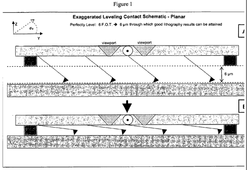
Figure 1. A Schematic showing a perfectly planar 2D nano PrintArray at the
intial point of
contact, and after 6 m of deflection grounding out on the standoffs. In this
embodiment, the
F.O.T. was 6 gm.
Figure 2. A schematic of a scenario where the 2D nano PrintArray approaches
the limit of
angular tolerance.
Figure 3. A flowchart illustrating the steps of leveling using NSCRIPTOR.
Figure 4. INKCAD display of the z-piezoelectric extender, actuator, sensor ("z-
piezo")
extension and retraction values and the icons in InkFinder.
Figure 5. (A) Mapping the visual progression of cantilever deflection for a
single viewport.
The array was first over-driven into the surface, and then deflection was
monitored as the
array was retracted. This provides a visual reference so that thereafter there
is no need to
extend more than 5 m beyond the "first contact" point; (B) SEM top angled view
of the
etched viewports; (C) SEM view from the underside showing three cantilevers in
front of the
viewport aperture; with the device mounted on the NSCRIPTOR scanner, the
NSCRIPTOR
optics was used to observed the cantilevers through the viewport both (D)
before the tips
touch the gold surface, and (E) after contact is made.
Figure 6. An illustration of planarity, with respect to an array chip and a
substrate, and the
parameters used to define thereof.
CA 02714005 2010-08-04
WO 2009/099619 PCT/US2009/000728
Figure 7. A SEM image of a 2D nano PrintArray with a F.O.T of 19.5 pm and the
array
shows significant "bowing."
Figure 8. Viewport configuration with respect to pivot point and total array
size and an
example of the estimation of the parameters used to defined planarity.
Figure 9. Simplified calculations of the approximated ratios for the
correction of the z-
difference between viewports.
Figure 10. A flowchart illustrating the steps of microscale leveling using the
INKLEVELER
including use of piezoelectric extender, actuator, or sensor.
Figure 11. Display of the default configurations and blueprint of the
hardware.
Figure 12. Display of the default configurations and blueprint of the 2D nano
PrintArray
device.
Figure 13. Display of the main 2D leveling software interface: (A) as it
appears by default,
waiting for user input; (B) the user has entered invalid z-probe input, with
the "execute
leveling" button remaining disabled; (C) the user has entered valid data, but
the array requires
further leveling - "execute leveling" button is enabled; (D) the entered z-
probe values
indicate the array is level, and the user can either execute leveling again;
or (E) proceed to the
"minimum amount past touchdown" table, which then appears and populated with
real data.
Figure 14. A table providing some examples of viewport touch-down data.
Figure 15. Display of the interactive manual z-piezo control, allowing the
user to control the
z-piezo position.
Figure 16. Optical micrograph of patterning result with unleveled array of
cantilever tips.
Figure 17. Optical micrograph of patterning result with array of cantilever
tips after the
array was leveled by leveling technique described in the presently claimed
invention.
DETAILED DESCRIPTION
INTRODUCTION
All references cited herein are hereby incorporated by reference in their
entirety.
Priority US provisional application serial no. 61/026,196 filed February 5,
2008 to
Haaheim et al. is hereby incorporated by reference in its entirety.
Two-dimensional pen arrays, including methods of making, are described in for
example US provisional application 60/792,950 filed April 19, 2006 to Mirkin
et al., which is
hereby incorporated by reference in its entirety including figures, claims,
and working
examples. See also the present specification, Figures 3-5 for related devices
and methods.
6
CA 02714005 2010-08-04
WO 2009/099619 PCT/US2009/000728
See also Salaita et al., Angew. Chem. Int. Ed., 2006, 45, 7220-7223; Lenhert
et al., Small,
2007, 3(l), 71-75, which are hereby incorporated by reference in their
entirety. In some of
the embodiments, the 2D array can be called "2D nano PrintArray."
For practice of the various embodiments described herein, lithography,
microlithography, and nanolithography instruments, pen arrays, active pens,
passive pens,
inks, patterning compounds, kits, ink delivery, software, and accessories for
direct-write
printing and patterning can be obtained from Nanolnk, Inc., Chicago, IL.
Instrumentation
includes the NSCRIPTOR. Software includes INKCAD software (Nanolnk, Chicago,
IL),
providing user interface for lithography design and control. E-Chamber can be
used for
environmental control. Dip Pen Nanolithography and DPN are trademarks of
Nanolnk,
Inc.
The following patents and co-pending applications related to direct-write
printing
with use of cantilevers, tips, and patterning compounds are hereby
incorporated by reference
in their entirety and can be used in the practice of the various embodiments
described herein,
including inks, patterning compounds, software, ink delivery devices, and the
like:
1. U.S. Patent No. 6,635,311 to Mirkin et al., which describes fundamental
aspects of DPN
printing including inks, tips, substrates, and other instrumentation
parameters and
patterning methods;
2. U.S. Patent No. 6,827,979 to Mirkin et al., which further describes
fundamental aspects of
DPN printing including software control, etching procedures, nanoplotters, and
complex
and combinatorial array formation.
3. U.S. patent publication number 2002/0122873 Al published September 5, 2002
("Nanolithography Methods and Products Produced Therefor and Produced
Thereby"),
which describes aperture embodiments and driving force embodiments of DPN
printing.
4. U.S. regular patent application, serial no. 10/366,717 to Eby et al., filed
February 14,
2003 ("Methods and Apparatus for Aligning Patterns on a Substrate"), which
describes
alignment methods for DPN printing (published October 2, 2003 as
2003/0185967).
5. U.S. regular patent application, serial no. 10/375,060 to Dupeyrat et al.,
filed February 28,
2003 ("Nanolithographic Calibration Methods"), which describes calibration
methods for
DPN printing.
6. U.S. Patent Publication 2003/0068446, published April 10, 2003 to Mirkin et
al. ("Protein
and Peptide Nanoarrays"), which describes nanoarrays of proteins and peptides;
7
CA 02714005 2010-08-04
WO 2009/099619 PCT/US2009/000728
7. U.S. Regular Patent Application, Ser. No. 10/307,515 filed Dec. 2, 2002 to
Mirkin et al.
("Direct-Write Nanolithographic Deposition of Nucleic Acids from Nanoscopic
Tips"),
which describes nucleic acid patterning (PCT /US2002/038252 published June 12,
2003).
8. U.S. Regular Patent Application, Ser. No. 10/320,721 filed Dec. 17, 2002 to
Mirkin et al.
("Patterning of Solid State Features by Direct-Write Nanolithographic
Printing"), which
describes reactive patterning and sol gel inks (now published August 28, 2003
as
2003/0162004).
9. US Patent Nos. 6,642,129 and 6,867,443 to Liu et al. ("Parallel,
Individually Addressible
Probes for Nanolithography"), describing active pen arrays.
10. U.S. Patent Publication 2003/0007242, published January 9, 2003 to
Schwartz
("Enhanced Scanning Probe Microscope and Nanolithographic Methods Using
Same").
11. U.S. Patent Publication 2003/0005755, published January 9, 2003 to
Schwartz
("Enhanced Scanning Probe Microscope").
12. U.S. Patent Application 10/637,641 filed August 11, 2003, now published as
2004/0101469, describing catalyst nanostructures and carbon nanotube
applications.
13. U.S. Patent Application 10/444,061 filed May 23, 2003, now published as
2004/0026681
published February 12, 2004, and US patent publication 2004/0008330 published
January
15, 2004, describing printing of proteins and conducting polymers
respectively.
14. U.S. Patent Application 10/647,430 filed August 26, 2003, now US Patent
No. 7,005,378,
describing conductive materials as patterning compounds.
15. U.S. Patent Application 10/689,547 filed October 21, 2003, now published
as
2004/0175631 on September 9, 2004, describing mask applications including
photomask
repair.
16. U.S. Patent Application 10/705,776 filed November 12, 2003, now published
as
2005/0035983 on February 17, 2005, describing microfluidics and ink delivery.
17. U.S. Patent Application 10/788,414 filed March 1, 2004, now published as
2005/0009206
on January 13, 2005 describing printing of peptides and proteins.
18. U.S. Patent Application 10/893,543 filed July 19, 2004, now published as
2005/0272885
on December 8, 2005, describing ROMP methods and combinatorial arrays.
19. U.S. Patent Application 11/056,391 filed February 14, 2005, now published
as
2005/0255237 published on November 17, 2005, describing stamp tip or polymer
coated
tip applications.
8
CA 02714005 2010-08-04
WO 2009/099619 PCT/US2009/000728
20. U.S. Patent Application 11/065,694 filed February 25, 2005, now published
as
2005/0235869 on October 27, 2005, describing tipless cantilevers and flat
panel display
applications.
21. US Patent publication 2006/001,4001 published January 19, 2006 describing
etching of
nanostructures made by DPN methods.
22. WO 2004/105046 to Liu & Mirkin published December 2, 2004 describes
scanning
probes for contact printing.
23. US Patent Application "Active Pen Nanolithography," 11/268,740 to Shile et
al. filed
November 8, 2005 describes for example thermcompression bonding and silicon
handle
wafers.
Embodiments described in US patent application 11/848,211 filed August 30,
2007
for "USING OPTICAL DEFLECTION OF CANTILEVERS FOR ALIGNMENT" can be
used.
In addition, the following US provisional applications filed January 26, 2009,
can be
used in practice of embodiments described herein, including, for example,
61/147,448;
61/147,449; 61/147,45 1; and 61/147,452, including methods of coating tips,
methods of and
devices for leveling, methods of controlling the substrate, and biological
applications of
..arrays prepared by methods described herein.
DPN methods are also described in Ginger et al., "The Evolution of Dip-Pen
Nanolithography," Angew. Chem. Int. Ed. 2004, 43, 30-45, including description
of high-
throughput parallel methods. See also Salaita et al., "Applications of Dip-Pen
Nanolithography," Nature Nanotechnology, 2007, Advanced On-line publication
(11 pages);
Rosner et., " Dip pen nanolithography: Applications and functional
extensions," Dekker
Encyclopedia of Nanoscience and Nanotechnology," Taylor and Francis Group, New
York,
2005; Huck, "Self-assembly meets nanofabrication: Recent developments in
microcontact
printing and dip-pen nanolithography," Angewandte Chemie-International Edition
46, 2754-
2757, 2007; and Lenhert, "Materials integration by dip-pen nanolithography in
Nanotechnology", Nanoprobes, Vol. 2, WILEY-VCH Weinheim, Berlin, 2008.
Direct write methods, including DPN printing and pattern transfer methods, are
described in for example Direct- Write Technologies, Sensors, Electronics, and
Integrated
Power Sources, Pique and Chrisey (Eds), 2002.
The direct-write nanolithography instruments and methods described herein are
particularly of interest for use in preparing bioarrays, nanoarrays, and
microarrays based on
peptides, proteins, nucleic acids, DNA, RNA, viruses, biomolecules, and the
like. See, for
9
CA 02714005 2010-08-04
WO 2009/099619 PCT/US2009/000728
example, US Patent No. 6,787,313 for mass fabrication of chips and libraries;
5,443,791 for
automated molecular biology laboratory with pipette tips; 5,981,733 for
apparatus for the
automated synthesis of molecular arrays in pharmaceutical applications.
Combinatorial
arrays can be prepared. See also, for example, US Patent Nos. 7,008,769;
6,573,369; and
6,998,228 to Henderson et al.
Scanning probe microscopy is reviewed in Bottomley, Anal. Chem., 1998, 70,
425R-
475R. Also, scanning probe microscopes are known in the art including probe
exchange
mechanisms as described in, for example, US Patent No. 5,705,814 (Digital
Instruments).
Microfabri cation methods are described in for example Madou, Fundamentals of
Microfabrication, 2 d Ed., 2002, and also Van Zant, Microchip Fabrication, 5th
Ed., 2004.
INSTRUMENT
Instruments capable of nanopositioning and using piezoelectric extendors,
actuators,
and/or sensors are known in the art. The instrument can be for example an AFM
instrument
modified for dip pen nanolithography, or alternatively, a similar instrument
adapted directly
to do dip pen nanolithography. Instrument can be obtained for example from
Nanolnk
(Skokie, IL) including for example an NSCRIPTORTM.
In some embodiments, the instrument comprises at least one z-axis
piezoelectric
extender, actuator, or sensor and at least three z-axis motors, both of which
can be controlled
and monitored by a software routine that allows a user to input positional
information via a
user interface. An example of the instruments is described in the US
provisional application
60/916,979 filed May 9, 2007 to Amro et al. (see also, US regular application,
"Compact
Nanofabrication Apparatus," 12/116,908 filed May 7, 2008).
Instruments, arrays of tips, and tips can be adapted to have or to not have
cantilevers.
For example, a cantilever free system of an array of tips is described in, for
example, Huo et
al., Science, September 19, 2008, vol. 321, no. 5896, 1658-1660, which is
hereby
incorporated by reference.
SUPPORT STRUCTURE
The support structure can be adapted to support tips, cantilevers, and
cantilevers
comprising tips. A support structure can be formed for example from a Si wafer
using resist
layer and bottom side etch with gold deposition. In addition, US provisional
application
60/792,950 filed April 19, 2006 to Mirkin et al. describes support structures,
which is hereby
CA 02714005 2010-08-04
WO 2009/099619 PCT/US2009/000728
incorporated by reference in its entirety (as is US regular application
11/690,738 filed March
23, 2007).
Particularly important design features include, for example, the heights of
the silicon
ridges and edge standoff spacers which help prevent crushing tips against the
underside of the
silicon handle wafer.
The support structure in some cases can be fabricated so that it is difficult
to view the
cantilevers without the presence of the viewports. For example, the support
structure may be
fabricated from a non-transparent material which does not allow viewing or
fabricated from a
material such as pyrex which might in principle be transparent but is
scratched, or roughened
or otherwise used in a way that does not allow viewing. The transparent
material can
become non-transparent through surface roughening and/or chemical etching, for
example.
The support structure can be also described with use of the term "handle
wafer."
The support structure also can be adapted for coupling to a larger instrument.
The
coupling is not particularly limited but can be for example a mechanical
coupling, or a
magnetic coupling. A structure adapted for this coupling can be attached to
the support
structure. For example, a plastic clip adapted with magnetic material can be
used.
The support structure can be fabricated from single crystal silicon. Advantage
over
pyrex for example includes etching holes through pyrex can be difficult or
expensive or
provide surface irregularities which interfere with bonding to cantilevers.
Single crystal
silicon provides for easier control of the etching.
The support structure can comprise base rows for supporting the cantilevers.
Base
row length is not particularly limited. For example, the base rows can have an
average length
of at least about 1 mm. Average length for base row can be, for example, about
0.1 mm to
about 5 mm, or about 0.5 mm to about 3 mm. In one embodiment, an array can be
made
which is about 1 cm by 1 cm and has a base row length of about 10 mm. If base
row length
becomes too long, one can be limited by bowing of support structure which can
exceed the
tip height and can keep all tips from touching the writing surface. Base row
length can be
adapted for each application to avoid this.
The base rows can have a height with respect to the support of at least about
5
microns. This height is not particularly limited but can be adapted for use
with the
appropriate cantilever bending. The height of the base row can be at or taller
than the tip
height minus the stop height to keep from crushing tips with overtravel.
The cantilevers can be supported on the base rows, and the base rows in turn
can be
supported on a larger support structure for the array. The base rows can
extend from the
11
CA 02714005 2010-08-04
WO 2009/099619 PCT/US2009/000728
larger support for the array. The array support can be characterized by a
surface area which
is about two square cm or less, or alternatively about 0.5 square cm to about
1.5 square cm.
The size can be adjusted as needed for coupling with an instrument.
Support structures can be made of silicon, pyrex, glass, plastic, soft
polymers such as
siloxane polymers including polydimethylsiloxane.
ARRAY OF CANTILEVERS AND TIPS
One or two dimensional arrays of cantilevers can be used.
The 2D array of cantilevers are known in the art. For example, US provisional
application 60/792,950 filed April 19, 2006 to Mirkin et al., US provisional
application
60/894,657 filed March 13, 2007 to Haaheim, and US 11/690738 filed on March
23, 2007 to
Mirkin et al., describe two dimensional arrays of cantilevers.
The two-dimensional array can be a series of rows and columns, providing
length and
width, preferably substantially perpendicular to each other. The arrays can
comprise a first
dimension and a second dimension. The two-dimensional array can be a series of
one
dimensional arrays disposed next to each other to build the second dimension.
The two
dimensions can be perpendicular. The cantilevers can comprise a free end and a
bound end.
The cantilevers can comprise tips at or near the free end, distal from the
bound end. The
cantilevers of one row can point in the same direction as the cantilevers on
the next row, or
the cantilevers of one row can point in the opposite direction as the
cantilevers on the next
row.
The two-dimensional arrays can be fabricated into a larger instrumental device
by
combining two parts, each part having a surface which is patterned in two
dimensions and
adapted to be mated with each other in the two dimensions. One part can
comprise the
support structure, without cantilevers, whereas the other part can comprise
the cantilevers.
One important variable is the fraction or percentage of the cantilevers in the
array
which can actually function for the intended purposes. In some cases, some
cantilevers can
be imperfectly formed, or can be otherwise damaged after formation. A
cantilever yield
reflects this percentage of usable cantilevers. Preferably, the array is
characterized by a
cantilever yield of at least 75%, or at least 80%, or at least 90%, or at
least 95%, or more
preferably, at least about 98%, or more preferably at least 99%. In
characterizing the
cantilever yield, cantilevers at the ends of rows may be neglected which are
damaged by
processing of edges compared to internal cantilevers. For example, the central
75% can be
measured. In many cases, the fabrication will be better done in the middle
rather than the
12
CA 02714005 2010-08-04
WO 2009/099619 PCT/US2009/000728
edge as edge effects are known in wafer fabrication. Defect density can
increase in some
cases as one moves from the center to the edge, or in other cases as one moves
from edge to
center. One can remove parts which have too high defect density and use
remaining parts.
The array can be adapted to prevent substantial contact of non-tip components
of the
array when the tips are brought into contact with a substantially planar
surface. For example,
the cantilever arms should not contact the surface and can be accordingly
adapted such as by,
for example, bending. The tips can be adapted for this as well including, for
example, long or
tall tips. Factors which can be useful to achieve this result include use of
long or tall tips,
bending of the cantilever arms, tip leveling, row leveling, and leveling of
the cantilevers in all
dimensions. One or more combination of factors can be used.
The cantilever tips can be relatively long or tall as known in the art. For
example, the
tips can have an apex height relative to the cantilever of at least four
microns on average, and
if desired, the tips can have an apex height relative to the cantilever of at
least seven microns
on average. In addition, tip apex height can be at least 10 microns, or at
least 15 microns, or
at least 20 microns. No particular upper limit exists and technology known in
the art and
improviding can be used. This long length can help ensure that only tips are
contacting the
surface. Apex height can be taken as an average of many tip apex heights, and
in general,
apex height is engineered not to vary substantially from tip to tip. Methods
known in the art
can be used to measure tip apex height including methods shown in the working
examples.
In measuring parameters for the array, average measurements can be used.
Average
measurements can be obtained by methods known in the art including for example
review of
representative images or micrographs. The entire array does not need to be
measured.
Tipless cantilevers can be used in some embodiments, although not a preferred
embodiment.
In addition, the cantilevers can be bent including bent towards the surface to
be
patterned. Methods known in the art can be used to induce bending. The
cantilevers can be
bent at an angle away from the base and the support. The cantilevers can
comprise multiple
layers adapted for bending of cantilevers. For example, differential thermal
expansion or
cantilever bimorph can be used to bend the cantilevers. Cantilever bending can
be induced
by using at least two different materials. Alternatively, the same materials
can be used but
with different stresses to provide cantilever bending. Another method is
depositing on the
cantilever comprising one. material a second layer of the same material but
with an intrinsic
stress gradient. Alternatively, the surface of the cantilever can be oxidized.
The cantilevers
can be bent at an angle for example of at least 5 from their base, or at
least 10 from their
13
CA 02714005 2010-08-04
WO 2009/099619 PCT/US2009/000728
base, or at an angle of at least 15 from their base. Methods known in the art
can be used to
measure this including the methods demonstrated in the working examples.
Average value
for angle can be used. The cantilevers can be bent on average about 10 microns
to about 50
microns, or about 15 microns to about 40 microns. This distance of bending can
be measured
by methods known in the art including the methods demonstrated in the working
examples.
Average distance can be used. The bending can result in greater tolerance to
substrate
roughness and morphology and tip misalignment within the array so that for
example a
misalignment of about 20 microns or less or about 10 microns or less can be
compensated.
To facilitate bending, the cantilevers can comprise multiple layers such as
two
principle layers and optional adhesion layers and can be for example bimorph
cantilevers.
The cantilevers can be coated with metal or metal oxide on the tip side of the
cantilever. The
metal is not particularly limited as long as the metal or metal oxide is
useful in helping to
bend the cantilevers with heat. For example, the metal can be a noble metal
such as gold.
In some embodiments, the array can be adapted so that the cantilevers are both
bent
toward the surface and also comprise tips which are longer than normal
compared to tips used
merely for imaging.
The tips can be fabricated and sharpened before use and can have an average
radius of
curvature of, for example, less than 100 nm. The average radius of curvature
can be, for
example, 10 nm to 100 nm, or 20 nm to 100 nm, or 30 nm to 90 nm. The shape of
the tip
can be varied including for example pyramidal, conical, wedge, and boxed. The
tips can be
hollow tips or contain an aperture including hollow tips and aperture tips
formed through
microfabri cation with microfluidic channels passing to end of tip. Fluid
materials can be
stored at the end of the tips or flow through the tips.
The tip geometry can be varied and can be for example a solid tip or a hollow
tip.
WO 2005/115630 (PCT/US2005/014899) to Henderson et al. describes tip
geometries for
depositing materials onto surfaces which can be used herein.
The tips can be made with polymers including soft polymers like siloxane
polymer.
The two dimensional array can be characterized by a tip spacing in each of the
two
dimensions (e.g., length dimension and width dimension). Tip spacing can be
taken, for
example, from the method of manufacturing the tip arrays or directly observed
from the
manufactured array. Tip spacing can be engineered to provide high density of
tips and
cantilevers. For example, tip density can be at least 10,000 per square inch,
or at least 40,000
per square inch, or at least 70,000 per square inch, or at least 100,000 per
square inch, or at
least 250,000 per square inch, or at least 340,000 per square inch, or at
least 500,000 per
14
CA 02714005 2010-08-04
WO 2009/099619 PCT/US2009/000728
square inch. The array can be characterized by a tip spacing of less than 300
microns in a
first dimension of the two dimensional array and less than 300 microns in a
second dimension
of the two dimensional array. To achieve even higher density, the tip spacing
can be, for
example, less than about 200 microns in one dimension and less than about 100
microns, or
less than about 50 microns, in another dimension. Alternatively, the tip
spacing can be for
example less than 100 microns in one dimension and a less than 25 microns in a
second
direction. The array can be characterized by a tip spacing of 100 microns or
less in at least
one dimension of the two dimensional array. In one embodiment, tip spacing can
be about 70
microns to about 110 microns in one dimension, and about 5 microns to about 35
microns in
the second dimension. There is no particular lower limit on tip spacing as
fabrication
methods will allow more dense tip spacing over time. Examples of lower limits
include 1
micron, or 5 microns, or 10 microns so for example tip spacing can be one
micron to 300
microns, or one micron to 100 micron.
The number of cantilevers on the two dimensional array is not particularly
limited but
can be at least about three, at least about five, at least about 250, or at
least about 1,000, or at
least about 10,000, or at least about 50,000, or at least about 55,000, or at
least about
100,000, or about 25,000 to about 75,000. The number can be increased to the
amount
allowed for a particular instrument and space constraints for patterning. A
suitable balance
can be achieved for a particular application weighing for example factors such
as ease of
fabrication, quality, and the particular density needs.
The tips can be engineered to have consistent spacing for touching the surface
consistently. For example, each of the tips can be characterized by a distance
D spanning the
tip end to the support, and the tip array is characterized by an average
distance D' of the tip
end to the support, and for at least 90 % of the tips, D is within 50 microns
of D'. In another
embodiment, for at least 90 % of the tips, D is within 10 microns of D'. The
distance
between the tip ends and the support can be for example about 10 microns to
about 50
microns. This distance can comprise for example the additive combination of
base row
height, the distance of bending, and the tip height.
Cantilever force constant is not particularly limited. For example, the
cantilevers can
have an average force constant of about 0.001 N/m to about 10 N/m, or
alternatively, an
average force constant of about 0.05 N/m to about 1 N/m, or alternatively an
average force
constant of about 0.1 N/m to about 1 N/m, or about 0.1 N/m to about 0.6 N/m.
The cantilevers can be engineered so they are not adapted for feedback
including
force feedback. Alternatively, at least one cantilever can be adapted for
feedback including
CA 02714005 2010-08-04
WO 2009/099619 PCT/US2009/000728
force feedback. Or substantially all of the cantilevers can be adapted for
feedback including
force feedback. For example, over 90%, or over 95%, or over 99% of the
cantilevers can be
adapted for feedback including force feedback.
The cantilevers can be made from materials used in AFM probes including for
example silicon, polycrystalline silicon, silicon nitride, or silicon rich
nitride. The cantilevers
can have a length, width, and height or thickness. The length can be for
example about 10
microns to about 80 microns, or about 25 microns to about 65 microns. The
width can be for
example 5 microns to about 25 microns, or about 10 microns to about 20
microns. Thickness
can be for example 100 nm to about 700 nm, or about 250 rim to about 550 rim.
Tipless
cantilevers can be used in the arrays, the methods of making arrays, and the
methods of using
arrays.
Arrays can be adapted for passive pen or active pen use. Control of each tip
can be
carried out by, for example, piezoelectric, capacitive, electrostatic, or
thermoelectric
actuation.
The arrays can be adapted for integration of tip coating and ink delivery. For
example, microfluidics can be used to control inking and coating of the tips.
Tips can be
dipped into devices or ink can be delivered directly through internal regions
of the tip for
hollow tip embodiments.
An important embodiment is that the cantilevers can be bonded to the support
structure via gold thermocompression bonding. Important factors can be an
inherent force
independence of the lithographic process based on cantilever tip deposition
and use of low k
flexible cantilevers including silicon nitride cantilevers.
Arrays of tips can be fabricated free of cantilevers.
Tips can be adapted to have various tip sizes, arrangements, numbers,
sharpnesses,
densities, and materials.
VIEWPORT
Fabrication and use of viewports are described in, for example, US serial no.
12/073,909 filed March 11, 2008 to Haaheim et al., which is hereby
incorporated by
reference in its entirety.
Figures 1 and 2 illustrate a concept of the viewport or opening wherein the
underlying
cantilever can be viewed through the support structure through a viewport or
an opening.
The viewport can be adapted to allow viewing. In turn, viewing can allow
leveling.
For example, depth, shape, length, and the width of the viewport can be
adapted to allow
16
CA 02714005 2010-08-04
WO 2009/099619 PCT/US2009/000728
viewing. If for example, a viewport were too long or too narrow, viewing may
become more
difficult or not possible. The viewport can be tapered which facilitates
viewing or imaging
the cantilevers from the opposite side. The top area of the viewport can be
larger than the
bottom area of the viewport. This can allow enough light to reach the
substrate surface and
cantilever to illuminate the contact point and reflect off the SiN cantilever,
providing a color
change which can be used to know when the tip or tips are touching the
surface. The top of
the opening can be wide enough so that blurring at the top is not an issue
when focusing on
the bottom.
A plurality or cluster of viewports can be present. For example, the support
structure
can provide at least two, or at least three, or at least four, or at least
five, or at least six
viewports. The number of viewports can be adapted in view of the larger
instrumental
structure. For example, the number of viewports can be correlated with the
number of motors
used to level the cantilever array. For example, one could use at least one
viewport per
motor, or use two viewports per motor.
The plurality or cluster of viewports can be adapted and arranged to fit
within the
optical viewing area of a nanolithography instrument such as the Nanolnk
NSCRIPTOR.
The appearance of the cantilevers can change when they are in two different
states: above the
,surface and in contact with the surface (Figure 5D and 5E, respectively). The
changes can be
due to different reflection of light permitted by open viewports. Image
recognition software
can be used as needed to detect changes.
The viewports can comprise sloping walls. The sloping walls can be
characterized by
an angle of slope. For example, a slope angle can be determined by the etching
of crystalline
silicon (e.g, 54.7 degrees). The viewports can comprise a variety of shapes
including for
example a pyramidal shape.
The shape of the viewport is not particularly limited as long as it can be
made and can
allow for viewing. The size of the viewport can be varied for an application
as needed. For
example, a lateral dimension of the viewport at the first side (away from the
cantilevers) such
as width can be for example about one micron to about 1,000 microns, or about
250 microns
to about 750 microns. The viewport can be sufficiently small so that the
structure is not
destabilized. The viewport dimensions can be limited by the pitch of the
ridges in one
direction, but laterally can be unlimited in for example another direction.
Viewing through the viewport can be facilitated with optical devices such as a
microscope. For example, microscopes can be used which are used in AFM and
similar
devices. The microscope can have for example a long working distance lens. The
Nanolnk
17
CA 02714005 2010-08-04
WO 2009/099619 PCT/US2009/000728
NSCRIPTOR lens can be for example a l OX objective lens. An onboard camera can
be used
with further zoom capability. The resulting video image can be for example
about 300
microns X about 400 microns.
Another advantage of a viewport is that it can provide laser access which for
example
can allow laser feedback from the cantilevers.
One can use the viewports first to work in a sacrificial area of a substrate
to for
example perform leveling and surface checks and then later move to a
patterning area.
NON-VIEWPORT EMBODIMENTS
Viewports can enable good function, although good function can be achieved
without
use of viewports. One can identify a point of reference in x-y. With a
transparent or
translucent handle chip/wafer, one can look through it at three or more
different points in x-y
to determine planarity. If electrical contact is used, one can measure contact
at three different
x-y points.
LEVELING PRIOR TO LITHOGRAPHY
Because the 2D nano PrintArray device is often imperfectly parallel (level) to
the
substrate, a pertinent question during processing becomes how to achieve and
verify uniform
contacts of all of the tips, or many or a majority of the tips, without
driving the corners of the
array into the sample, which would lead to sample scratching, pattern
distortion, and/or
arraying fishtailing during lithography. The "levelness" (or "planarity") of
the 2D nano
PrintArray with respect to the substrate can be described in terms of the
relative z positions of
three distinct points on the 2D nano PrintArray as measured by z-axis motors,
or as two
relative angular difference measurements as measured by goiniometer motors
(i.e., (p, 0). A
schematic illustration of these parameters is provided in Figure 6.
The concept of Freedom of Travel (F.O.T.) can be particularly important in
this
process. Figure 1 illustrates this concept for one embodiment in which a
planar 2D nano
PrintArray with 6 m F.O.T., where (A) illustrates a "feather touch" situation
(where the tips
are just beginning to touch the substrate), and (B) illustrates the "hard
crunch" (where the
cantilevers have gone through their full 6 m freedom of travel, and the array
is now
grounding out on the standoffs). Thus, in this embodiment, initial z-
positioning of anywhere
from 0.1 to 5.9 m within the F.O.T. can yield excellent lithography with
uniform contact,
while the extreme of 0.0 pm can lead to no writing (i.e., no contact), and 6.0
m can lead to
18
CA 02714005 2010-08-04
WO 2009/099619 PCT/US2009/000728
distorted writing (standoffs grounding out). In other words, in this
embodiment, after making
first contact (i.e., uniform contact) with the substrate, there was a 6.0 m
margin of error
before grounding out on the standoffs. A scanning electron microscopy (SEM)
image of
another embodiment of the 2D nano PrintaArray with a F.O.T. of 19.5 m is
provided in
Figure 7. Note that the F.O.T. of a cantilever can be limited in principle
mostly by the length
of the cantilever itself; for example, if the cantilever is perpendicular to
the substrate, then
F.O.T. is the length of the cantilever.
Figure 2 illustrates a situation where the 2D nano PrintArray was not
perfectly planar,
but still within the tolerance to achieve uniform writing. (1) and (2) show
that by the time
first contact was observed in the "lowest" viewport, the cantilevers at the
edge of the device
have already deflected 2.30 m. Cantilever deflection can be monitored for
example by
observing how and when the cantilevers naturally change color; one example of
this color
change is shown in Figure 5. According to (3), after another 1.40 m, the
"highest" viewport
was deflecting, but there was still another 2.30 m to deflect until all the
cantilevers tips were
uniformly touching (4), thereafter there would be no margin of error, and the
standoff was
nearly touching the substrate.
In the embodiment where the F.O.T. is 6.0 m, the differences in z-positions
between
the highest and lowest viewports, as well as one angular difference
measurement A(p2, can be
estimated with the approximation shown in Figure 8. These measurements can
then provide
an indicator of the amount the motors need to be moved to improve planarity;
Figure 9
illustrates an example of a first order approximation of the ratios of the
difference in z-
different as observed by the viewports to the amount of motors need to be
moved. In general,
the higher the F.O.T. of the array and the smaller the z-difference between
"highest" and
"lowest" viewports, the easier it was to achieve uniform contact and
lithography.
LEVELING WITH SOFTWARE ROUTINE AND USER INTERFACE
One leveling approach that has been employed involves bringing the scanner in
contact with the device on the sample surface with a small amount of epoxy.
One
disadvantage of this method is that epoxy takes about one hour to dry and can
introduce
volume distortion, which in turn could adversely affect leveling. Generally,
leveling is
performed by correcting the differences in the z-height obtained by generally
a combination
of visual inspection and measuring the motors positions.
19
CA 02714005 2010-08-04
WO 2009/099619 PCT/US2009/000728
The presently claimed inventions can generally eliminate the use of epoxy and
provides a user-friendly computer interface, allowing the operator of the
leveling instrument
to gain device planarity efficiently and accurately. The user interface can be
part of the
software routine, which can be called, for example, INKLEVELER, which can be
operated
within an instrument such as, for example, NSCRIPTOR. Examples of the software
interface
are provided in Figure 11 and 12, wherein a display of the default
configurations and
blueprint of the hardware and that of the 2D nano PrintArray, respectively,
are illustrated.
Together with visual inspection of the device planarity, the routine provides
a microscale
leveling method for the device that can be iterative, utilizing both the
motors and particularly
the z-piezoelectric extender, actuator, or sensor ("z-piezo") to provide
better measurements of
the differences in the z-height among the viewports, and providing a more
accurate means to
minimize these differences. It is noted that the instrument need not only
comprise of one z-
piezo; it can comprise two, three, or more z-piezos as needed. A exemplary
flowchart is
provided in Figure 3 to summarize the leveling steps involved in one of the
embodiments.
Illustrating examples of the user interface and detailed descriptions of the
software routine
are provided in the embodiments.
Note that the capabilities of the software, in combination of the leveling
hardware
.instrumentation, need not be limited by those described herein. In fact, one
important feature
of the presently claimed inventions can be the potential for the software to
be adapted or be
adaptable for future modifications, further improving its functionality. For
example, the
image recognition method for cantilever deflection can be improved to provide
better
detection of the deflection, thereby improving the planarity of the array. The
sensing
capability of the piezoelectric extender, actuator, or sensor can also be
improved via better
instrumentation or operational control through the software. Additionally,
conductive sensors
can be used as the sensing instrumentation. Moreover, the software can be
adapted to
provide automated measurements with minimal user input and/or automated
iterative
calculations during leveling.
MACROSCALE LEVELING ("EYEBALLING")
This method can provide a means to level the substrate macroscopically,
relying on a
human naked eye's ability to maneuver the 2D nano PrintArray within about 500
and about
800 m of the substrate and to use the z-motors to make corrections to account
for gross
planar misalignment. It is meant to provide an approximation and is generally
performed
CA 02714005 2010-08-04
WO 2009/099619 PCT/US2009/000728
prior to the subsequent microscale leveling. It is noted that the number of
viewports, and
hence the, number of motors controlling alignment of the substrate can be
three, four, five, or
more.
In one embodiment, macroscale leveling was accomplished via the following
steps:
1. A backlight reflector was attached to the scanner assembly to aid in
eyeballing.
Kimwipe was taped and draped behind the puck of the NSCRIPTOR scanner
(Nanolnk,
Inc.) to further aid visual inspection. Note that any lightly colored surface
may be used for
this purpose. The puck and array were optionally taken out, and the scanner
was optionally
pulled out of its cartridge assembly. The puck, array, and scanner assembly
were returned
upon completion of this step.
2. The 2D nano PrintArray was mounted on the scanner. The scanner was returned
to its home position in the cartridge, and all of the z-axis motors were at
the tops of their
individual ranges. The sample puck was in place, with an about 1 x 2 cm2
sample loaded.
The array was positioned in X-Y over the 1 cm2 "sacrificial" planar alignment
area of the
substrate.
3. The optics were adjusted to bring the cantilevers of one viewport (for
example,
viewport 1 a) into focus; the camera was zoomed.
4. A flexible LED illuminators was placed on the NSCRIPTOR stage. The setup
was positioned such that maximum backlighting (i.e., so that the Kimwipe
sheets glow a
uniformly white color) was obtained.
5. The large scale motor corrections were estimated to bring the array closer
to
alignment.
6. The z-all position (i.e., position of the entire array) was moved down in
increments of 100 m.
7. As the 2D nano PrintArray got closer to the substrate, angular differences
were
corrected subsequently to improve alignment.
8. Each eye of the user was kept on the level of the substrate and
perpendicular to the
array along the horizontal axis. Combinations of one eye viewing with the
other closed (used
for enhancement of lateral accuracy) and two eye viewing (used for enhancement
of
perspective) were employed.
9. A mirror was inserted perpendicularly to the y-axis to double check
planarity
along the x-axis.
21
CA 02714005 2010-08-04
WO 2009/099619 PCT/US2009/000728
10. Motor corrections were initiated, and if necessary, they were applied to
individual motors.
11. The adjustments applied to each motor were recorded.
12. Once the array is about 100 .im above the surface, microscale leveling was
employed.
MICRO-LEVELING THROUGH THE VIEWPORTS
In some embodiments, leveling was performed via NSCRIPTOR instrument
(Nanolnk, Inc) in conjunction with at least one array comprising at least one
cantilever
optionally further comprising tips. Upon completion of macroscale leveling,
the cantilever
deflection was monitored and controlled by the motors and the z-piezo through
the viewports
to bring leveling within the tolerances dictated by the device's important or
critical
dimensions. An exemplary flowchart is provided in Figure 10 to summarize one
example of
the iterative process. Note that the iterative calculations were performed by
the software
routine, and the entire process need only be performed once for the same
assembly.
In one embodiment, the micro-leveling procedure can be described as follows:
1. After the 2D nano PrintArray was leveled via eyeballing, the LED backlight
illuminators and the laser attached to the scanner were turned off to conserve
battery life.
2. The extend value of the z-piezo was set to 10 V by creating a 5 second
dwell time
in the INKCAD software. A graphical illustration of a INKCAD interface is
provided in
Figure 4. The z-piezo was extended using the "Pen Down" button.
3. The optics over any one of the three viewports were positioned to lower the
PrintArray onto the substrate surface using 20, 10, and then 5 m steps in
order to map the
cantilever deflection. It was noted that from roughly 100 m down to about 10
m above the
substrate, the cantilevers underwent a gradual color shift, as illustrated in
Figure 5; however,
once near the surface and in contact, the color shift became dramatic.
4. The observed deflection behavior is provided in Figure 5. Note that this is
just
one of several possible examples of cantilever deflection - others can become
more distinct
varieties of yellow, green, and/or pink, depending on the lighting and the
angle of viewing.
The working range of the motor motion and the corresponding cantilever
deflection were
verified by applying a 25-30 m displacement back and forth several times.
Additionally, the
method of detection is not limited to observing a change of color; for
example, any apparent
change of visual appearance, such as intensity of reflection or extent of
cantilevers'
22
CA 02714005 2010-08-04
WO 2009/099619 PCT/US2009/000728
uncurling, can be used. Because the NSCRIPTOR optics had significant backlash
components, the cantilevers had to be frequently refocused to observe
deflection.
5. After the relative deflection characteristics of the cantilevers at each
viewport
have been identified, the user chose any one of the viewports and bring the
array into contact
with the surface. Note that the user can choose any viewports, but to
facilitate identification,
the first to be chosen was named the "1" group, the second "2" group, and the
third "3"
group. Note that the leveling can be more accurate if the user used the outer
ring B
viewports.
6. In each viewport, the z-all position (i.e., position of the entire array)
was used to
make rough measurements of the deflections at the three different viewports.
The "z-probe"
value was read from the "probe z-position" indicator on the interface panel,
and the z-all
position was provided when a given viewport showed deflection. The result of
this step is
shown in the Figure 13.
7. A control button such as "Execute leveling" was pressed, and the entire
array (z-
all position) was lifted off the surface by 100 m, whereupon the individual z-
axis motors
corrected their positions based upon the input z-probe values. Thereafter the
array returned
to within about 20 m above the surface.
8. At the same viewport, the array was brought back into contact with the
surface
using z-all. The z-piezo was fully extended, and all of the viewports showed
some amount of
deflection. Figure 15 provides an exemplary display of the user interface
prompting the user
to enter the z-piezo position. It was ascertained that none of the viewports
showed deflection
when the z-piezo was fully retracted.
9. At each viewport, the z-piezo position tool was used to make fine
measurements
of three different viewport's deflections. The z-all was not adjusted. The z-
probe value thus
was the sum of the static "probe z-position" and the dynamic z-piezo position.
10. If the user entered invalid z-probe values, the "execute leveling" button
remained
disabled; if the user entered valid data but the array required further
leveling, the "execute
leveling" button was enabled; if the probe values indicated that the array was
already level,
the user could proceed to next step or repeat step 9 (see Figure 13). Note the
user can always
repeat step 9 to achieve increasingly fine degrees of planarity.
11. Z-all was withdrawn 20 m, and the z-piezo was fully extended.
12. The viewport with the clearest deflection characteristics was focused, and
the t-
all was lowered until those cantilevers began to deflect.
23
CA 02714005 2010-08-04
WO 2009/099619 PCT/US2009/000728
13. The amount indicated in Figure 14 was entered as the "minimum amount past
touchdown" on the user interface (Figure 13E) to ascertain all the tips were
uniformly
touching the surface. The amount was provided by the software.
14. The z-piezo was fully retracted to bring all of the tips out of contact.
Lithography commenced.
Note that laser was not used for any part of planar leveling. The normal tip
approach
routines, as provided by the AFM operation software, were not used for as part
of planar
leveling, either.
Figure 16 (A-B) provides an example of the patterning result without employing
the
leveling described herein, as observed via optical microscopy.. The area of
the 1 cm2 2D nano
PrintArray was illustrated as a box. In some of the figures it could be seen
that patterning did
not occur due to a lack of contact between the cantilever tips and the
substrate. Also, the
lines X patterns in Figure 16(B) were not very straight.
By contrast, Figure 17 (A-B) provides an example of the patterning result
after the
micro-leveling was performed. Patterning occurred for almost every cantilever
on the array,
and the lines of the X patterns were straighter and sharper. Note that the
gaps in Figure 17(B)
were attributed to broken tips, rather than a lack of cantilever tip contact
with the substrate.
In a variety of embodiments, as a result of the micro-leveling, at least 50% ,
preferably at least 70%, more preferably at least 90%, or even more preferably
at least 95%
of the non-broken tips touched the substrate and contributed to patterning.
The leveling techniques described herein can provide a fast and accurate
method to
level the substrate, thereby providing uniform contacts between the cantilever
tips and the
substrate to improve reproducibility and accuracy of printing or patterning
process.
ADDITIONAL EMBODIMENTS
Different embodiments can be present for determining point of contact. These
include, for example, cantilever deflection, any observable color change from
a tip or from a
cantilever, sign of movement in the x-y plane representing skidding,
deformation or change
of shape (particularly, for example, if translucent polymer tips are used),
change in size,
focus, or shading. Human judgement or image recognition software can be used
to determine
point of contact.
Specific ranges can be determined for the point of contact. A degree of
accuracy can
be determined such as, for example, 200 nm or 100 nm.
24
CA 02714005 2010-08-04
WO 2009/099619 PCT/US2009/000728
In another embodiment, the cantilever and tip can be engineered to provide one
or
more bright spots near or at the tips which can be monitored for an indicator
of when the tip
touches the surface, or the point of contact. For example, in one embodiment,
a ratio of
stoichiometric to low stress SiN in bimorph configuration can be adapted to
provide bright
spots. For example, a thickness ratio can be about 1,000:3,000 in angstroms.
In addition,
freedom of travel and curl can be adapted also to control the bright spots.
Registration to existing surface features can be carried out. For example, the
tip can
be aligned in the x-y directions to existing locations with respect to the
substrate.
Substrate size can be varied for the application. For example, a substrate can
be at
least one square mm, or at least five square mm, or at least 25 square mm.