Note: Descriptions are shown in the official language in which they were submitted.
CA 02714203 2010-09-01
OPTOELECTRONIC RANGE FINDER
RELATED APPLICATION
This application claims the benefit of CN 200910034550.4, filed on September
1, 2009,
the disclosure of which is incorporated herein by reference in its entirety.
BACKGROUND
Optoelectronic range finders are widely used in the field of architecture,
indoor decoration,
and the like due to their ability to provide high measurement accuracy. Such
devices typically
include an emitter which emits modulated beams that may be reflected or
dispersed by an object
to be measured and an optoelectronic receiver. Currently, there are two
methods for measuring
the distance between the optoelectronic range finder and the object to be
measured. One method
is based on the phase measurement principle which determines the distance
between the
optoelectronic range finder and the object to be measured by using the phase
difference between
the modulated beams that are emitted and then received by the optoelectronic
receiver. The
second method is based on the flight time principle which calculates the
distance of the object to
be measured by using the flight time delay of the modulated beam when received
by the
optoelectronic receiver relative to when emitted from the emitter.
The measurement accuracy of such optoelectronic distance measurement devices
may,
however, be affected by the environment and the device itself, e.g., a
temperature change in the
environment and/or a temperature drift of the optoelectronic receiver.
Accordingly, the phase
drift due to the temperature change in the environment and/or the temperature
drift of the
CA 02714203 2010-09-01
optoelectronic receiver is currently eliminated by setting an inner reference
optical path with a
predetermined length within the optoelectronic distance measurement device. By
way of
example, U.S. Patent No. 5,949,531 discloses a system wherein the emitting
optical path is
provided with a mechanical converting device for switching the modulated beams
emitted from
the emitter between an outer optical measurement path and an inner reference
optical path
whereby the modulated beams transmitted through the outer optical measuring
path and the inner
reference optical path may be received by the optoelectronic receiver
successively to thereby
generate a low frequency measurement signal and a low frequency reference
signal, respectively.
The measurement error of the distance measuring device may then be eliminated
by the
subtraction of the phases of the low frequency measurement signal and the low
frequency
reference signal. This method may be performed many times in one measuring
process whereby
the measurement signal and the reference signal alternatively enter into the
optoelectronic
receiver by means of the mechanical converting device. However, the currently
utilized
mechanical converting device may experience a large mechanical load with a
result that the
mechanical converting device tends to become worn and damaged during the
process. Moreover,
the mechanical converting device complicates the inner structure of the
distance measuring device,
increasing the manufacturing cost as well as the size and the weight of the
distance measuring
device which is not helpful for the miniaturization development of the
distance measuring device.
By way of further example, U.S. Patent No. 6,917, 415 discloses a system
wherein the
emitting optical path is provided with a spectrometer device for dividing the
modulated beams
emitted from the emitter into two portions. One portion of the modulated beams
is projected to
2
CA 02714203 2010-09-01
the object to be measured through the outer optical measurement path and the
other portion of the
modulated beams are received by the optoelectronic receiver directly through
the inner reference
optical path. As before, a low frequency measurement signal and a low
frequency reference
signal are generated in the optoelectronic receiver. While this system
eliminates the
disadvantages of the above-described mechanical converting device, the energy
of the modulated
beams emitted to the object to be measured through the outer optical
measurement path is
decreased because a portion of the modulated beams are divided into the inner
reference optical
path thereby affecting the measurement ability of the device for
optoelectronic distance
measurement.
The emitter currently used in the optoelectronic range finder is generally a
semiconductor
laser which uses semiconductor material as the working medium. The
semiconductor materials
generally include GaAs, Cds and Zns. There are three actuation modes, that is,
electronic
injection, electron-beam actuation, and optical pumping. Referring to Figs. 1
and 2, Fig. 1 shows
the inner core structure of an exemplary GaAs semiconductor laser and Fig. 2
shows the package
structure of an exemplary GaAs semiconductor laser which includes the working
medium,
resonant chamber, and pumping source. The working medium refers to the GaAs
semiconductor
material with a band gap itself, which is also called a PN junction. The
resonant chamber
generally comprises two parallel planes which are vertical to the PN junction
plane, the two
planes are usually used as cleavage planes of the semiconductor crystal and
may be polished, and
the remaining two sides of planes are relatively rough and used for
eliminating the action of the
laser in other directions except for the main direction. The pumping source is
the current that is
3
CA 02714203 2010-09-01
fed by the PN junction.
Fig. 3 shows the principle of operation for the exemplary semiconductor laser.
In this
regard, the semiconductor laser achieves an inversion distribution of the
particle beam, and
generates stimulated radiation, by feeding current into the semiconductor PN
junction, and
achieves the optical amplification so as to generate laser oscillation by
means of the positive
feedback of the resonant chamber. As the resonant chamber of the semiconductor
laser is formed
via the cleavage planes of the semiconductor and the cleavage planes usually
have a reflectance of
35%, it is enough to induce laser oscillation. If the reflectance needs to be
increased, a silicon
dioxide coating may be plated on the crystal face, and then a metal coating
(silver) is plated
additionally thereof, thereby achieving a reflectance of more than 95%, thus
the two cleavage
planes may both emit laser light. In the current practice, the distance is
measured by the laser
beam emitted from one of the two cleavage planes which is called the main
laser beam. In order
to make sure that the output of the power of the main laser beam is not
affected by the temperature
change and voltage fluctuation, automatic compensation control for the power
of the main laser
beam is currently achieved by monitoring the luminous intensity of the laser
beam emitted from
the other cleavage plane which is called the compensating laser beam. A
photodiode is presently
added in the laser module to monitor the compensation laser beam, and the
output power of the
main laser beam is controlled to be constant by an external member. Fig. 4
shows the
semiconductor laser module in the prior art, wherein the laser module includes
a laser diode (LD)
and a photodiode (PD) wherein the two cleavage planes of the laser diode
respectively emit the
main laser beam and the compensation laser beam while the photodiode is used
to monitor the
4
CA 02714203 2010-09-01
luminous intensity of the compensation laser beam.
SUMMARY
In order to overcome the deficiencies in the prior art, hereinafter is
described an
optoelectronic range finder which has a high measurement ability that is
provided without the use
of a mechanical converting device.
More particularly, the subject optoelectronic range finder includes: an
emitter with a first
end for emitting a measuring light beam onto an object to be measured and a
second end; a
receiver for receiving the measuring light beam reflected or dispersed by the
object to be
measured and for converting the received light to a measurement signal; a
signal processing
device for filtering the measurement signal and a reference signal; and a
control and analysis
device for analyzing the information associated with the measurement signal
and the reference
signal so as to determine the distance of the object to be measured, wherein
the second end of the
emitter is used to emit a reference beam which is received by the receiver and
converted to the
reference signal. The described optoelectronic distance measurement device
would thus perform
the steps of. emitting a measuring light beam from a first end of an emitter
onto a object to be
measured where the measuring light beam is reflected or dispersed by the
object to be measured;
receiving the measuring light beam so reflected or dispersed by the object to
be measured and
converting it into a measurement signal; processing the measurement signal and
comparing it with
a reference signal; and determining the distance of the object to be measured
based on the
information of the measurement signal and the reference signal, wherein
another reference light
beam is emitted from a second end of the emitter, which is received and
converted into the
5
CA 02714203 2010-09-01
reference signal.
In the optoelectronic range finder and the method hereinafter described, a
measuring beam
and a reference beam are emitted from the first end and the second end of the
emitter respectively
whereby a measurement signal and a reference signal are correspondingly
generated in the
receiver and the distance of the object to be measured is determined based on
the information of
the measurement signal and the reference signal. In contrast to the prior art,
the hereinafter
described optoelectronic range finder needs no additional mechanical
converting device and will
not decrease the energy of the measuring beam emitted onto the object to be
measured, thereby
simplifying the structure of the measurement device and enhancing the accuracy
of the measuring
device.
BRIEF DESCRIPTION OF THE DRAWINGS
A preferred optoelectronic range finder will be in detail below in conjunction
with the
accompanied drawings in which:
Fig. I is a schematic view of the inner core structure of a prior art GaAs
semiconductor
laser;
Fig. 2 is a schematic view of the package structure of the GaAs semiconductor
laser of Fig.
1;
Fig. 3 is a schematic view of the principle of operation of the GaAs
semiconductor laser of
Fig. 1;
Fig. 4 is a schematic view of a prior art semiconductor laser module;
Fig. 5 is a schematic view of an exemplary semiconductor laser with double
laser beams
6
CA 02714203 2010-09-01
constructed according to the description that follows;
Fig. 6 is a view of an exemplary distance measurement device incorporating the
optoelectronic range finder of the semiconductor laser with double laser beams
of Fig. 5;
Fig. 7 is a schematic view of a semiconductor laser with double laser beams
that is
constructed according to another described embodiment; and
Fig. 8 is a view of a distance measurement device incorporating the
optoelectronic range
finder of the semiconductor laser with double laser beams of Fig. 7.
DETAILED DESCRIPTION
An optoelectronic range finder, which is also referred to as a device for
optoelectronic
distance measurement, uses a semiconductor laser with double laser beams as an
optical signal
emitter. As shown in Fig. 5, which is a schematic view of an exemplary
semiconductor laser
with double laser beams constructed according to one preferable embodiment,
the semiconductor
laser 10 with double laser beams emits a main laser beam 13 and a compensation
laser beam 14 at
the two cleavage planes 11, 12. The main laser beam 13 as the measuring beam
is projected onto
an object to be measured through an outer optical measurement path, and the
compensation laser
beam 14 is projected onto the optoelectronic receiver through an inner
reference optical path. In
the present embodiment, a photodiode (PD) for monitoring the power of the
laser is omitted, and
windows through which the main laser beam 13 and the compensating laser beam
14 can be
projected outward are provided at the exterior of the semiconductor laser 10
corresponding to the
position of the two cleavage planes 11, 12. In contrast to the prior art where
the laser emits a
laser beam at only one end, in the present embodiment, the semiconductor laser
10 with double
7
CA 02714203 2010-09-01
laser beams emit a laser beam at each of its two ends.
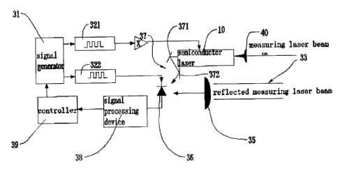
Fig. 6 is a view of a distance measurement device incorporating the device for
optoelectronic distance measurement of the semiconductor laser with double
laser beams shown
in Fig. 5. The semiconductor laser 10 emits at its one end the main laser beam
13, i.e., the
measuring laser beam, which is projected onto an object to be measured (not
shown) through an
outer measurement path 33 after being collimated by a collimating optical
element 40. Then, the
reflected measuring laser beam reflected or dispersed back from the object to
be measured is
received by an optical receiving element 35 and transmitted to an
optoelectronic receiver 36.
The semiconductor laser 10 also emits a compensation laser beam 14 at the
other end, i.e., the
reference laser beam, which is directed to an optoelectronic receiver 36
through a pair of reflex
elements 371, 372. The path that the reference laser beam 14 passes through
from the reflex
elements 371, 372 to the optoelectronic receiver 36 forms the well-known inner
reference optical
path 37.
A high frequency modulated signal 321 is transmitted to the semiconductor
laser 10 so as
to modulate the amplitude of the laser beam, which is generated by a signal
generator 31 and
output to the semiconductor laser 10 with double laser beams to modulate the
laser beam emitted
from the laser 10. With the laser beam modulated by the high frequency
modulated signal 321,
the reflected measuring laser beam received by optoelectronic receiver 36
through the outer
measuring path generates a high frequency measurement signal in the
optoelectronic receiver 36.
The signal generator 31 also generates a similar high frequency signal 322
which is transmitted to
the optoelectronic receiver 36 through a connection lead. The high frequency
measurement
8
CA 02714203 2010-09-01
signal in the optoelectronic receiver 36 and the high frequency signal 322 are
mixed so as to
generate a low frequency measurement signal. In this example, the
optoelectronic receiver 36
takes the form of an avalanche photodiode and may also be used as a mixer. If
a common
optoelectronic receiver is used, an additional mixer element can be used for
mixing the high
frequency measurement signal and the high frequency signal. Similarly, the
high frequency
reference signal received by the optoelectronic receiver 36 through the inner
reference optical
path 37 and the high frequency signal 322 are mixed to generate a low
frequency reference signal.
Certainly, it is easily conceivable for the skilled person in the art that
alternatives may be used for
receiving the high frequency reference signal.
The low frequency reference signal and the low frequency measurement signal
generated
successively in the optoelectronic receiver 36 are transmitted to a signal
processing device 38 to
be processed. Generally, in the signal processing device 38, the low frequency
measurement
signal and the low frequency reference signal are amplified and filtered,
thereby generating a low
frequency measurement signal and a low frequency reference signal containing
phase or time
information. In general, the signal is amplified by a transresistance
amplifier and the high
frequency signal part of the signal is filtered by a low pass filter. The low
frequency
measurement signal and the low frequency reference signal containing phase or
time information
that are processed by the signal processing device 38 are further transmitted
to the controller 39
which determines the distance from the device for optoelectronic distance
measurement to the
object to be measured based on the information of the low frequency
measurement signal and the
low frequency reference signal.
9
CA 02714203 2010-09-01
Fig. 7 is a schematic view of the semiconductor laser with double laser beams
according to
another preferable embodiment. In this embodiment, the semiconductor laser 20
with double
laser beams emits a main laser beam 23 and a compensation laser beam 24 at the
two cleavage
planes 21, 22. The main laser beam 23 as measuring beam is projected onto an
object to be
measured through an outer optical measurement path, and the compensation laser
beam 24 is
transmitted to a photodiode 25 which controls the output power of the main
laser beam 23 to be
constant by monitoring the compensation laser beam 24. In this embodiment, a
portion of the
compensation laser beam 24 as reference beam is directed to the optoelectronic
receiver by an
optical fiber 26. Fig. 8 is a view of an exemplary distance measurement device
incorporating the
device for optoelectronic distance measurement of the semiconductor laser with
double laser
beams shown in Fig. 7. The measurement principle is substantially the same as
that in preceding
embodiment, except that the semiconductor laser 20 with double laser beams
emits the measuring
laser beam 23 at one end, and at the other end is connected with the optical
fiber 26 which leads
from the laser 20 a portion of the compensation laser beam 24 as the reference
beam. The
reference beam transmitted through the optical fiber 26 is received by the
optoelectronic receiver
directly and generates a reference signal correspondingly. The path that the
reference beam
passes through from the optical fiber 26 to the optoelectronic receiver 36
constitutes the
well-known inner reference optical path.
Preferably, a light adjustment valve is additionally arranged in the reference
optical path in
the above two embodiments of the present invention. The light valve may adjust
the
transmission rate, and thereby controls the intensity of the reference beam
emitted at the other end
CA 02714203 2010-09-01
of the laser.
The detailed embodiments described above are intended to illuminate the
concepts and
principles of the present invention rather than limit the scope of the
invention herein after claimed.
In this regard, those skilled in the art will appreciate that many other
modifications and variations
of these preferred embodiments may be made without departing from the spirit
and the scope of
the invention as defined in the following claims.
ii