Note: Descriptions are shown in the official language in which they were submitted.
CA 02714511 2010-09-08
PRINTING PROCESS FOR ENHANCED JETTED PERFORMANCE OF
SEMICONDUCTOR LAYER
DETAILED DESCRIPTION
Field of Use
[0001] The present teachings relate generally to organic semiconductors and,
more particularly, to materials and methods for organic semiconductors having
enhanced printing performance.
Background
[0002] Semiconductor technology has played an important role in the
development of electronic circuits over the past several decades. Two examples
of semiconductor technology include complementary metal oxide semiconductor
(CMOS) processing technology and organic semiconductor processing
technology.
[0003] Organic semiconductor processing technology was developed more
recently, wherein organic materials that exhibit semiconducting properties are
used to fabricate electronic and optoelectronic devices on substrates that are
rigid
or flexible.
[0004] Compared to CMOS processing technology, organic semiconductor
processing technology is cheaper to implement and more suitable to specific
applications such as flexible electronics and displays. This is particularly
advantageous for large area displays and low-cost RFID tags.
[0005] Conventional methods for forming organic semiconductors include
printing a particle-containing dispersion onto a substrate. The printable
dispersion
1
CA 02714511 2010-09-08
is often a non-Newtonian fluid, in which the viscosity changes with applied
strain
rate. Such dispersion having a viscosity that is not well defined may cause
poor
jetted performance during printing. For example, significant offsets from
original
design are often observed for the printed organic semiconductor features,
including non-uniform or broken line or patterns, rough edges, etc.
[0006] Thus, there is a need to overcome these and other problems of the
prior art and to improve deposition performance of organic semiconductor
features.
SUMMARY
[0007] According to various embodiments, the present teachings include a
process for forming a semiconductor feature by first providing a liquid
composition
that includes one or more organic semiconductors. The liquid composition can
then be converted from a non-Newtonian form at a first temperature to a
Newtonian form at a second temperature. The converted liquid composition in
the
Newtonian form can then be deposited on a substrate to form one or more
semiconductor features.
[0008] According to various embodiments, the present teachings also include
a process for forming a semiconductor feature. In this method, a liquid
composition that includes a plurality of organic semiconductor particles
dispersed
in a solvent can be formed to have a shelf-life of more than about two days.
The
liquid composition can then be heated so as to uniformly dissolve the
plurality of
organic semiconductor particles in the solvent to form a Newtonian liquid
2
CA 02714511 2010-09-08
composition, which can then be printed onto a substrate to form one or more
uniform semiconductor features.
[0009] Additional objects and advantages of the present teachings will be set
forth in part in the description which follows, and in part will be obvious
from the
description, or may be learned by practice of the present teachings. The
objects
and advantages of the present teachings will be realized and attained by means
of
the elements and combinations particularly pointed out in the appended claims.
[0010] It is to be understood that both the foregoing general description and
the following detailed description are exemplary and explanatory only and are
not
restrictive of the present teachings, as claimed.
BRIEF DESCRIPTION OF THE DRAWINGS
[0011] The accompanying drawings, which are incorporated in and constitute
a part of this specification, illustrate several embodiments of the present
teachings
and together with the description, serve to explain the principles of the
present
teachings.
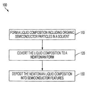
[0012] FIG. 1 depicts an exemplary method for forming an organic
semiconductor feature in accordance with various embodiments of the present
teachings.
(0013] FIG. 2 depicts an exemplary printing system for forming an organic
semiconductor feature in accordance with various embodiments of the present
teachings.
3
CA 02714511 2010-09-08
[0014] FIG. 3 depicts an exemplary rheological test result for an exemplary
non-Newtonian liquid composition in accordance with various embodiments of the
present teachings.
[0015] FIG. 4 depicts a conversion from non-Newtonian to Newtonian of an
exemplary liquid composition in accordance with various embodiments of the
present teachings.
[0016] FIGS. 5A-5B schematically depict exemplary semiconductor features
Jetted in a non-Newtonian form in accordance with various embodiments of the
present teachings.
[0017] FIGS. 6A-6B schematically depict exemplary semiconductor features
jetted in a Newtonian form in accordance with various embodiments of the
present
teachings.
[0018] It should be noted that some details of the FIGS. have been simplified
and are drawn to facilitate understanding of the embodiments rather than to
maintain strict structural accuracy, detail, and scale.
DESCRIPTION OF THE EMBODIMENTS
[0019] Reference will now be made in detail to embodiments of the present
teachings, examples of which are illustrated in the accompanying drawings.
Wherever possible, the same reference numbers will be used throughout the
drawings to refer to the same or like parts.
[0020] In the following description, reference is made to the accompanying
drawings that form a part thereof, and in which is shown by way of
illustration
specific exemplary embodiments in which the present teachings may be
practiced.
4
CA 02714511 2010-09-08
These embodiments are described in sufficient detail to enable those skilled
in the
art to practice the present teachings and it is to be understood that other
embodiments may be utilized and that changes may be made without departing
from the scope of the present teachings. The following description is,
therefore,
merely exemplary.
[0021] Exemplary embodiments provide materials and processes for forming
organic semiconductor features. In one embodiment, the formation of
semiconductor features can include a rheological conversion of a liquid
composition between a non-Newtonian "dispersion" having an un-defined
viscosity
and a Newtonian "solution" having a constant viscosity. In embodiments,
uniform
semiconductor features can be formed with improved deposition performance.
[0022] FIG. 1 depicts an exemplary process for forming a semiconductor
feature in accordance with various embodiments of the present teachings. While
the process 100 of FIG. 1 is illustrated and described below as a series of
acts or
events, it will be appreciated that the present invention is not limited by
the
illustrated ordering of such acts or events. For example, some acts may occur
in
different orders and/or concurrently with other acts or events apart from
those
illustrated and/or described herein. Also, not all illustrated steps may be
required
to implement a methodology in accordance with one or more aspects or
embodiments of the present invention. Further, one or more of the acts
depicted
herein may be carried out in one or more separate acts and/or phases.
[0023] At 110 of FIG. 1, a liquid composition can be formed by dispersing one
or more semiconductor materials in a suitable organic solvent.
CA 02714511 2010-09-08
[0024] In embodiments, the semiconductor material can include one or more
organic semiconductors having a formula (I) of the following:
R2
S A
S t)n
R1
(I)
wherein A is a divalent linkage; R1 and R2 is independently selected from the
group consisting of hydrogen, alkyl, arylalkyl, alkylaryl, perhaloalkyl,
alkoxyalkyl,
siloxy-substituted alkyl, polyether, alkoxy, and halogen; and n is from 2 to
about
5,000.
[0025] In embodiments, the divalent linkage A of formula (I) can include a
structure selected from the following:
6
CA 02714511 2010-09-08
R' R' R'
S
S S e S R'
R' R' R
R'
R' R R
R' R' R'
I
\ / \ j \ \ I \ \ \ O N
R' R' Rl R' / N O
R'
R' R'
S S / \ \
S
R' R' R'
R'
S S
R, S S
R'
S S S
R' R, S A
I R,
R'
7
CA 02714511 2010-09-08
R'
/ / O N O
N N S
R'
S
and combinations thereof, wherein each R' is independently selected from the
groups consisting of hydrogen, alkyl, substituted alkyl, aryl, substituted
aryl,
heteroaryl, halogen, -CN, and -NO2.
[0026] In further embodiments, the semiconducting material can include a
compound having the following formula:
R2
S \ S
S S n
R1 (II)
8
CA 02714511 2010-09-08
R1 R,
s
R" R2
n
(III),
R1
/ \ S R'
S \ S
R" S
R2
n
(iv)
9
CA 02714511 2010-09-08
R2 R,
S S
/ S C! I\
R" S
IT
n
(V)
[/s\S/s/1S1fl
R"
R2
(VI), and
S S R' Ri
LR' S S \S/ S n
R2
(VII)
wherein R1, R2, R', and R" are independently selected from i) hydrogen, ii)
alkyl or
substituted alkyl, iii) aryl or substituted aryl, iv) alkoxy or substituted
alkoxy, v) a
suitable hetero-containing group, vi) a halogen, or mixtures thereof; and n is
an
integer from about 2 to about 5,000, from about 2 to about 2,500, from about 2
to
about 1,000, from about 100 to about 800, or from about 2 to about 100. The
CA 02714511 2010-09-08
hydrocarbon can be alkyl, alkoxy, aryl, substituted derivatives thereof, and
the like,
inclusive of side-chains containing, for example, from zero to about 35 carbon
atoms, or from about 1 to about 30 carbon atoms, or from about 1 to about 20
carbon atoms, or from about 6 to about 18 carbon atoms.
[0027] In embodiments, R1 and R2 can be the same or different and each
independently selected from a long carbon side-chain containing from about 6
to
about 30 carbon atoms, or from about 6 to about 20 carbon atoms; and R' or R"
can be the same or different and each independently selected from a
substituent
containing from 0 to about 5 carbon atoms; or R1 and R2 can be each
independently selected from a substituent containing from 0 to about 5 carbon
atoms, and R' can be a long carbon side-chain containing from 6 to about 30
carbon atoms.
[0028] In embodiments, R, and R2, R', and R" can independently be alkyl with
about 1 to about 35 carbon atoms of, for example, methyl, ethyl, propyl,
butyl,
pentyl, hexyl, heptyl, octyl, nonyl, decyl, undecyl, dodecyl, tridecyl,
tetradecyl,
pentadecyl, hexadecyl, heptadecyl or octadecyl; or arylalkyl with about 7 to
about
42 carbon atoms of, for example, methylphenyl (tolyl), ethyiphenyl,
propylphenyl,
butylphenyl, pentylphenyl, hexylphenyl, heptylphenyl, octylphenyl,
nonylphenyl,
decylphenyl, undecylphenyl, dodecylphenyl, tridecylphenyl, tetradecyiphenyl,
pentadecylphenyl, hexadecyiphenyl, heptadecylphenyl, and octadecylphenyl. In
other embodiments, R1, R2, R' and R" can independently represent alkyl or
substituted alkyl groups having from about 1 to about 35 carbon atoms.
[0029] In a specific embodiment, the semiconducting material can be a
compound having the following formula:
11
CA 02714511 2010-09-08
C12H25
(s) )S) S n
C12H25
(1),
C12H25 C12H25
s s
C12H25 C12H25
n
(2),
C14H29
s I \
s s
H29C14 n
(3),
S C15H31
S S
C15H31 S
(4),
12
CA 02714511 2010-09-08
C8H17
r--,-C10H21
O N O
i i S
S
O N O n
C1oH21
C8H17
(5),
C14H29
C14H29 s \ S
S NN S
S S C14H29
C14H29
(6),
N N
S S
C12H25 C122H5 C12H25C12H25 n
(7),
13
CA 02714511 2010-09-08
C13H27 s s
S s
S S C13H27
n
($),
C8H17
N
S / \ S/
S S \
C12H25 C12H25
(9),
C16H33C16H33
N- S,
/SN
s s
n
(10), and
s
S s s s
C 1[2H25C12H25
n
(11).
14
CA 02714511 2010-09-08
The number average molecular weight (Mn) of the polymers in embodiments can
be, for example, from about 500 to about 400,000, including from about 1,000
to
about 150,000, and the weight average molecular weight (Mw) thereof can be
from about 600 to about 500,000, including from about 1,500 to about 200,000,
both as measured by, for example, gel permeation chromatography using
polystyrene standards.
[0030] In a specific embodiment, the semiconducting material can be a
compound of the formula (1). In another specific embodiment, the
semiconducting
material can be a compound of the formula (2) to (5).
[0031] In embodiments, the type of solvent used can result in effective mixing
or dispersion of the semiconductor materials in the solvent. In embodiments,
the
solvent can be an aromatic solvent. In some embodiments, the solvent can be a
halogenated aromatic solvent. Exemplary halogenated aromatic solvents can
include chlorobenzene, dichlorobenzene (1,2-dichlorobenzene, and 1,3-
dichlorobenzene), trichlorobenzene, or chiorotoluene. In a specific
embodiment,
the solvent can include 1,2-dichlorobenzene. In some embodiments, the solvent
can be a non-halogenated solvent. Exemplary non-halogenated aromatic solvents
can include toluene, xylene, mesitylene, trimethylbenezene, ethylbenzene,
tetrahydronaphthalene, and the like. In some embodiments, the solvent can be a
non-aromatic solvent. Exemplary non-aromatic solvent can include chloroform,
chioroethane, cyclohexane, bicyclohexyl and the like.
[0032] In an exemplary embodiment, the liquid composition can include
poly(3,3"'-dialkyl-quaterthiophene) (PQT-12) dispersed in an exemplary solvent
of
dichlorobenzene.
CA 02714511 2010-09-08
[0033] In embodiments, in addition to organic semiconductors, the liquid
composition can be formed to further include, for example, any suitable
nanomaterials including, such as nanotubes, nanowires nanodots, quantum dots,
nanorods, nanocrystals, nanotetrapods, nanotripods, nanobipods, nanoparticles,
nanosaws, nanosprings, nanoribbons, and/or any other suitable nanomaterials or
combination of nanomaterials to improve the carrier mobility and conductivity
of
the formed semiconductors.
[0034] In embodiments, high temperatures that are above ambient
temperature (e.g., about 20-25 C) can be used to facilitate the
dispersion/dissolution of organic semiconductors in the solvent. This can be
followed by a cooling process to form the liquid composition at the ambient
temperature. In embodiments, any suitable processes, such as, for example,
sonication or mechanical stirring, can be used to facilitate the
dispersion/dissolution of organic semiconductors in the solvent.
[0035] For example, organic semiconductors can be dissolved in the solvent
at an elevated temperature of, for example, up to about 80 C depending on the
organic semiconductors and the solvent used. The dispersion can then be formed
by cooling the solution to room temperature (about 20-25 C) to form the
liquid
composition, wherein the dissolved organic semiconductors aggregate, for
example, into nano structures in the solvent. In embodiments, the dispersion
can
be ultra-sonicated, for example, during cooling.
[0036] In embodiments, organic semiconductors can form semiconductor
particles, such as, semiconductor aggregates or semiconductor nanoparticles in
the solvent. As a result, the formed liquid composition containing
semiconductor
16
CA 02714511 2010-09-08
particles can be non-Newtonian having an un-defined viscosity. That is, the
viscosity of the liquid composition containing semiconductor particles can
change
as a shear force applies to the liquid composition.
[0037] In various embodiments, the non-Newtonian liquid composition
containing semiconductor particles can be stable at a first temperature
ranging
from 0 to about 50 C, including the temperature from about 0 C to about 40 C
or
from about 20 C to about 40 C. In addition, the non-Newtonian liquid
composition containing semiconductor particles can have a long shelf-life, for
example, at least about two days. Other embodiments can include a stable non-
Newtonian liquid composition having a long shelf-life of, for example, up to
about 1
year or longer. The stability of the non-Newtonian liquid composition at the
first
temperature can allow for easy storage and transfer prior to further
processing.
[0038] In various embodiments, semiconductor particles in the non-
Newtonian liquid composition can include various shapes, regular or irregular,
and
various dimensions. For example, the semiconductor particles can include
aggregates in a nanometer scale having at least one minor dimension of about
1000 nm or less. In embodiments, the semiconductor nanoparticles in the non-
Newtonian liquid composition can be in various forms, regular or irregular,
including, but not limited to, nanotubes, nanofibrils, nanorods, nanobelt,
nanoshafts, nanopillars, nanowires, nanoneedles or their combinations.
[0039] In various embodiments, from about 0.5% to about 100% of the
semiconductor in the non-Newtonian liquid composition can be nano aggregates.
In some embodiments, at least about 30% of the semiconductor in the non-
Newtonian liquid composition can be nano aggregates. In other embodiments,
17
CA 02714511 2010-09-08
from about 50 % to about 80% of semiconductor in the non-Newtonian liquid
composition can be nano aggregates.
[0040] In various embodiments, if non-Newtonian liquid composition
containing the semiconductor particles is directly deposited onto a substrate,
for
example, jetted onto the substrate, undesired defects may be observed because
the shear viscosity of the non-Newtonian liquid composition may change in the
print-head when being jetted at high frequency.
[0041] At 120, the non-Newtonian liquid composition formed at step 110 can
be temporarily converted into a Newtonian liquid composition. That is, stress
versus rate of strain curve of the liquid composition can be linear and pass
through
the origin. The Newtonian liquid composition can thus have a constant
viscosity
determined by constant of that proportionality.
[0042] Various techniques can be used to conduct such rheological
conversion of the liquid composition. For example, the non-Newtonian liquid
composition can be converted into a Newtonian liquid composition by a heating
process, or other suitable processes, in embodiments. The heating process can
be conducted, for example, using elevated temperatures or in a step-wise
manner.
In embodiments, the heating temperature can be selected depending on a
conversion temperature between a non-Newtonian state and a Newtonian state of
certain liquid compositions.
[0043] In various embodiments, the conversion temperature can in turn be
determined by, e.g., measuring the rheological properties of the liquid
composition. For example, an oscillatory measurement can be used to measure
the complex viscosity of a non-Newtonian liquid composition as function of the
18
CA 02714511 2010-09-08
temperature. The conversion temperature can be a starting temperature or a
temperature range when the complex viscosity of the liquid composition becomes
constant, which means the liquid composition becomes a uniform Newtonian
solution. During this conversion, semiconductor particles can be uniformly or
completely dissolved in the solvent and, in some cases, no aggregates or
particles
can be observed in the uniform Newtonian solution. In certain embodiment, the
Newtonian solution can be substantially absent of aggregates or particle of
the
organic semiconductor.
[0044] In various embodiments, the non-Newtonian liquid composition can be
heated to a second temperature. The second temperature can be the conversion
temperature (or the conversion temperature range) or be greater than the
conversion temperature (or the conversion temperature range) of a specific
liquid
composition. In exemplary embodiments, the non-Newtonian liquid composition
can be heated at elevated temperatures from about 20 C to about 120 C or in
some cases from about 40 C to about 120 C. In other exemplary embodiments,
the non-Newtonian liquid composition containing semiconductor particles can be
heated for a conversion at elevated temperatures ranging from about 45 C to
about 80 C.
[0045] The non-Newtonian liquid composition containing semiconductor
particles can then be converted into a uniform solution of Newtonian liquid
composition.
[0046] In embodiments, such conversion can be performed in a time period
of, for example, less than about 1 hour. In some embodiments, the conversion
from a non-Newtonian form to a Newtonian form can take about 30 minutes less
19
CA 02714511 2010-09-08
and in some embodiments about 10 minutes or less. In further embodiments,
quick conversion can be achieved of about 1 minute or less.
[0047] In embodiments, after the conversion, the Newtonian liquid
composition can be equilibrated for a period of time, such as about 1 hour or
less.
In some embodiments, the Newtonian liquid composition can be equilibrated for
about 30 minutes less or in some embodiments about 10 minutes or less. In
other
embodiments, the Newtonian liquid composition can be equilibrated for about 1
minute or less. In embodiments, the liquid composition can be kept at the
second
temperature for a short time so as to avoid the degradation of organic
semiconductors.
[0048] In various embodiments, other conversion temperatures, conversion
temperature ranges, and/or equilibration times can be used, depending on
materials and methods used for the liquid composition.
[0049] In various embodiments, the heating can be performed by using a
heater, for example, an oven, a radiant energy source, a thermocouple, or a
combination thereof.
[0050] At 130 of FIG. 1, the Newtonian liquid composition can be deposited
into semiconductor features on a substrate. The deposited semiconductor
features can then be solidified or dried, for example, by an evaporation or a
heating process. Various semiconductor features, such as semiconductor layers,
patterns, lines or dots, can then be formed.
[0051] In various embodiments, the deposition can be performed using a
printing or a coating technique. Exemplary printing techniques can include
inkjet
printing, lithographic or offset printing, flexographic printing, screen
printing, stencil
CA 02714511 2010-09-08
printing, stamping, micro-contact printing, gravure, and the like. Exemplary
coating techniques can include spin coating, blade coating, rod coating, dip
coating, and the like. In one embodiment, the deposition can be inkjet
printing.
[0052] In embodiments, during deposition of the Newtonian liquid
composition, a predetermined array can be designed in order to form an array
of
semiconductor features including for example, the semiconductor layers,
patterns,
lines or dots as described above.
[0053] In embodiments, each semiconductor feature in the resulting array
may have an offset, i.e., a center-to-center spacing, from its original
design. In
embodiments, the offset can range from 0 to about 30 microns, or in some
embodiments, from 0 to about 20 microns. In other embodiments, the offset
between a formed semiconductor feature and its original design can be less
than
about 10 microns.
[0054] FIG. 2 depicts an exemplary system 200 for printing semiconductor
features in accordance with various embodiments of present teachings. It
should
be readily apparent to one of ordinary skill in the art that the system 200
depicted
in FIG. 2 represents a generalized schematic illustration and that other
components/ devices can be added or existing components/ devices can be
removed or modified.
[0055] As shown in FIG. 2, the system 200 can include a printable substrate
205, and a printing station including a cartridge 210, one or more print-heads
220
each having a jet nozzle 225, and a heater 230.
21
CA 02714511 2010-09-08
[0056] The cartridge 210 can be used for supplying ink dispersion, in
embodiments, such as the non-Newtonian liquid composition containing
semiconductor particles.
[0057] The heater 230 can be configured with the print-heads 220 and/or the
jet nozzle 225 so as to heat the non-Newtonian liquid composition that passes
the
print-heads 220 and/or the jet nozzle 225. In this manner, the non-Newtonian
liquid composition dispersion containing semiconductor particles can be
converted
in-situ into a Newtonian liquid composition solution.
[0058] In embodiments, due to the Newtonian feature of the liquid
composition, the occurrence of clogging of the ink-jet nozzles can be
minimized,
and the uniformity of the printing or the jetting as well as the uniformity of
deposited semiconductor features can be achieved.
[0059] The heated non-Newtonian liquid composition can then be jetted
through the jet nozzle 225 onto a printable substrate 205. The printable
substrate
205 can be configured to receive the jetted liquid composition to form
semiconductor features through, for example, a drying process.
[0060] In one embodiment, prior to the deposition of the Newtonian liquid
composition, the surface of the printable substrate can be chemically treated
or
mechanically rubbed. In embodiments, the printable substrate can be an organic
substrate, an inorganic substrate, a flexible substrate or a rigid substrate.
In
embodiments, the printable substrate can include, for example, glass, silicon
(including electrode bearing silicon substrates), polyimide, polyethylene
terephthalate (PET), poly(ethylenenaphthalate) (PEN), indium tin oxide (ITO),
or
any other suitable substrate.
22
CA 02714511 2010-09-08
[0061] In embodiments, the substrate can be at a third temperature. The
third temperature can be, for example, from about 0 to about 120 C, including
from about 20 C to about 80 C, or from about 20 C to about 40 C. In
further
embodiments, the third temperature can be similar to the first temperature,
for
example, to be lower than the conversion temperature of the liquid
composition.
In other words, the Newtonian fluid can become non-Newtonian fluid when it
reaches the substrate. That is, nano-aggregates or gel can be re-formed at the
substrate. In view the whole process, the liquid composition can undergo a
phase
change from non-Newtonian state (having nano aggregates phase, or the
dispersion phase) to a Newtonian state (substantially absent of nano
aggregates
in the solution phase), and back to non-Newtonian state (having nano
aggregates
phase, or the dispersion phase). This phase change printing process can enable
high accuracy jetting at Newtonian state, and low spreading or well confined
drops
of the liquid composition upon the substrate due to the reversion to the non-
Newtonian state. The feature of non-Newtonian ink fluid having high viscosity
at
low shear rate can facilitate to confine the ink drops and to reduce
spreading.
[0062] In embodiments, the process 100 and/or system 200 disclosed herein
can be used for forming devices such as, for example, transistors, sensors,
light
emitting diodes, photovoltaic devices, or any other suitable device or
combination
of devices.
[0063] The following examples are illustrative of the invention and its
advantageous properties, and are not to be taken as limiting the disclosure or
claims in any way.
[0064] Examples
23
CA 02714511 2010-09-08
[0065] Example 1- Organic Semiconductor PQT
[0066] Organic semiconductor PQT was used as an exemplary organic
semiconductor for forming semiconductor features. The organic semiconductor
POT had the following structure:
R
[S) S
S S
n
R
PQT-12, R= C12H25
[0067] Example 2- PQT-Dispersion or Non-Newtonian Liquid
Composition Containing PQT Semiconductor Particles
[0068] The non-Newtonian liquid composition containing POT semiconductor
particles was prepared by dissolving PQT-1 2 semiconductor in a solvent of 1,2-
dichlorobenzene at an elevated temperature of up to about 80 C, followed by a
cooling process. During cooling, the particle dispersion was sonicated. Purple
color dispersion containing PQT and/or nano-PQT particles was obtained, which
was very stable at room temperature, for example, having a shelf-life over
about 1
year.
[0069] Rheological properties of the PQT-dispersion were measured using
RFS3 Fluids Spectrometer (TA Instruments, New Castle, Delaware) with a cone
and plate geometry. Ti (titanium) based cone was used with a nominal cone
angle
of 0.02 radians and a gap of 48.3 microns.
24
CA 02714511 2010-09-08
[0070] A steady rate sweep test was performed for the PQT-dispersion at
about 25 C and at a frequency ranging from 1 to 1000 s-1. FIG. 3 shows
measured results, which indicate that the PQT-dispersion is a non-Newtonian
fluid. Specifically, FIG. 3 shows the PQT-dispersion has a shear thinning
property
(or a pseudoplastic property), i.e., having high viscosity (e.g., over 100
cps) at low
shearing rates and having low viscosity (e.g., about 2-3 cps) at high shearing
rates
(e.g., about 103S-1).
[0071] Example 3- Conversion from a Non-Newtonian Form to a
Newtonian Form
[0072] Small amplitude oscillatory measurement was conducted for the PQT-
dispersion of Example 2, wherein the Non-Newtonian dispersion was heated at an
elevated temperature from about 25 C to about 65 C with a temperature
increment
of about 2 C. Each increased temperature had an equilibration time of about
120
seconds.
[0073] During this rheological oscillatory measurement, a constant frequency
of about 1 Hz was used. As shown in FIG. 4, when the PQT-dispersion was
gradually heated from room temperature to about 40 C, the complex viscosity
is
gradually decreased. The complex viscosity however becomes constant once the
temperature was increased at about 40 C or greater, e.g., up to about 65 C
in
this example, showing a Newtonian characteristic. In other words, the
exemplary
PQT-dispersion had a conversion temperature or a narrow conversion
temperature range at around 40 C for changing from a non-Newtonian dispersion
into a Newtonian solution.
CA 02714511 2010-09-08
[0074] Example 4 - Semiconductor Features Jetted at Non-Newtonian
Form
[0075] Dimatix inkjet printer equipped with 10 pL cartridges was used in this
comparative (or control) example. The print-head was set at room temperature.
PQT-dispersion of Example 2 was deposited at a non-Newtonian form. A 4X4 cm
dot-array spaced by 100 m, and two straight lines each having single-drop
width
were designed and printed as examples.
[0076] FIGS. 5A-5B depict exemplary semiconductor features Jetted at a
non-Newtonian form in accordance with various embodiments of the present
teachings.
[0077] Specifically, FIG. 5A schematically depicts the jetted results of dot-
array. As shown, mis-directional deposition was observed although most of the
area showed a regular dots array similar to the designed pattern. FIG. 5B
schematically depicts the jetted results of thin lines. Rough edges and/or
broken
area were also observed for this non-Newtonian PQT-dispersion of Example 2.
[0078] Example 5 -Semiconductor Features Jetted at Newtonian Form
[0079] In this example, same printer and cartridges were used as for Example
4. The print-head of the cartridges was set at 60 C, which is higher than the
convention temperature as indicated by Example 3. Therefore, when the PQT-
dispersion of Example 2 passed through the print-head, the particle dispersion
can
be changed into Newtonian solution that was then jetted out of the nozzles.
Same
pattern designs shown in FIGS. 5A-5B were printed for comparison purpose.
26
CA 02714511 2010-09-08
[0080] FIGS. 6A-6B depict exemplary semiconductor features jetted at a
Newtonian form in accordance with various embodiments of the present
teachings.
[0081] Specifically, FIG. 6A schematically depicts the jetted results of dot-
array. As shown, no misfired drop was observed for the whole 4X4 cm array.
FIG. 6B schematically depicts the jetted results of thin lines. As shown, the
printed lines were observed to be smooth and uniform, without any broken area.
[0082] As compared with FIGS. 5A-5B, FIGS. 6A-6B indicates high quality
semiconductor prints or semiconductor features achieved by using the disclosed
processes and systems.
[0083] While the present teachings have been illustrated with respect to one
or more implementations, alterations and/or modifications can be made to the
illustrated examples without departing from the spirit and scope of the
appended
claims. In addition, while a particular feature of the present teachings may
have
been disclosed with respect to only one of several implementations, such
feature
may be combined with one or more other features of the other implementations
as
may be desired and advantageous for any given or particular function.
Furthermore, to the extent that the terms "including", "includes", "having",
"has",
"with", or variants thereof are used in either the detailed description and
the claims,
such terms are intended to be inclusive in a manner similar to the term
"comprising." As used herein, the term "one or more of with respect to a
listing of
items such as, for example, A and B, means A alone, B alone, or A and B. The
term "at least one of is used to mean one or more of the listed items can be
selected.
27
CA 02714511 2010-09-08
[0084] Notwithstanding that the numerical ranges and parameters setting
forth the broad scope of the present teachings are approximations, the
numerical
values set forth in the specific examples are reported as precisely as
possible.
Any numerical value, however, inherently contains certain errors necessarily
resulting from the standard deviation found in their respective testing
measurements. Moreover, all ranges disclosed herein are to be understood to
encompass any and all sub-ranges subsumed therein. For example, a range of
"less than 10" can include any and all sub-ranges between (and including) the
minimum value of zero and the maximum value of 10, that is, any and all sub-
ranges having a minimum value of equal to or greater than zero and a maximum
value of equal to or less than 10, e.g., 1 to 5. In certain cases, the
numerical
values as stated for the parameter can take on negative values. In this case,
the
example value of range stated as "less than 10" can assume values as defined
earlier plus negative values, e.g. -1, -1.2, -1.89, -2, -2.5, -3, -10, -20, -
30, etc.
[0085] Other embodiments of the present teachings will be apparent to those
skilled in the art from consideration of the specification and practice of the
present
teachings disclosed herein. It is intended that the specification and examples
be
considered as exemplary only, with a true scope and spirit of the present
teachings being indicated by the following claims.
28