Note: Descriptions are shown in the official language in which they were submitted.
CA 02714539 2010-09-09
238491
APPARATUS FOR CONNECTING A MULTI-CONDUCTOR CABLE TO A PIN
GRID ARRAY CONNECTOR
BACKGROUND OF THE INVENTION
This invention relates generally to an apparatus for connecting a multi-
conductor
cable to a pin grid array connector.
Electronic devices are often connected to other electronic devices by the use
of one or
more cables and connectors. In many such cases, the connectors, cables, and
devices
are standardized for universal type connections. For instance, a computer
monitor
having a standardized VGA connector can be connected to a personal computer
having a standardized VGA connector by a standardized cable with standardized
mating VGA connectors on both ends. Given this standardization, most any
monitor
can connect to most any personal computer as long as both were built within a
certain
time range because all or almost all commonplace varieties of personal
computers and
monitors built in the same approximate time period include standardized VGA
connectors.
On the other hand, specialty electronic devices (e.g., driving electronics for
testing
devices such as phased array ultrasonic instrumentation) available from
different
manufacturers often have different types of connectors to connect to
corresponding
electronic devices. For example, a testing device available from one
manufacturer
can be operated or controlled through a multi-conductor cable (e.g., 16, 32,
64, or 128
conductors) extending from the testing device to a number of different
possible
driving electronic devices, each built by a different manufacturer and each
using
different types of connectors for connecting to the multi-conductor cable.
With no
accepted standardization of connectors for these specialized devices (i.e.,
driving
electronics devices), multi-conductor cables linking the driving electronic
device to
the testing device must be custom-built to accommodate the particular
connector on
1
CA 02714539 2010-09-09
238491
the driving electronic device. The cables can be micro coaxial, and run
lengths up to
and exceeding 50 meters.
For example, a multi-conductor cable extending from a particular testing
device is
typically terminated by soldering each conductor onto one or more cable
terminating
printed circuit boards (PCBs), each of which also has a cable terminating
connector
for mating with the driving electronics device. Each cable terminating PCB can
have
circuitry for connecting a particular conductor from the multi-conductor cable
to a
particular electrical contact of the cable terminating connector. The type of
cable
terminating connector can be selected such that it mates directly with the
type of
connector of the driving electronic device. However, this requirement that the
cable
terminating connector directly mate with various types of driving electronic
device
connectors eliminates the possibility of creating a standardized multi-
conductor cable
extending from a particular testing device, since each multi-conductor cable-
to-
driving electronics connector interface must be customized based on the
different
types of connectors used for the driving electronic devices (e.g., must
terminate the
multi-conductor cable with different types of cable terminating connectors
depending
on the connectors of the driving electronics devices).
Included in these different types of connectors used for the driving
electronic devices
are at least two general categories: (i) connectors that can directly mate
with a PCB
surface mounted connector, and (ii) connectors that have a pin grid array that
cannot
directly mate with a PCB surface mounted connector.
As for the driving electronics device connectors that can directly mate with a
PCB
surface mounted connector, there are several different types (e.g., type X, Y,
or Z)
that can interface with a single type of cable terminating connector (e.g.,
type A)
through the use of PCBs, allowing for the use of a standardized multi-
conductor cable
(i.e., type of cable terminating connector (e.g., type A)) is not chosen based
on the
particular type of driving electronics device PCB surface mounted connector
(e.g.,
type X, Y, or Z)). For example, the multi-conductor cable extending from a
particular
testing device can be terminated by soldering each conductor onto one or more
cable
terminating PCBs, each of which has a type A cable terminating PCB surface
mounted connector. Each type A cable terminating PCB can have circuitry for
2
CA 02714539 2010-09-09
238491
connecting a particular conductor from the multi-conductor cable to a
particular
electrical contact of the type A cable terminating PCB surface mounted
connector.
Each type A cable terminating PCB surface mounted connector can then be
connected
to a mating type A connector interfacing PCB surface mounted connector mounted
on
another PCB referred to as a connector interfacing PCB. In addition to the
type A
cable terminating PCB surface mounted connector, each connector interfacing
PCB
also has a connector interfacing PCB surface mounted connector of a type that
mates
directly with the driving electronics connector (e.g., type X, Y, or Z). Each
connector
interfacing PCB can have circuitry for connecting a particular electrical
contact from
the type A connector interfacing PCB surface mounted connector to a particular
electrical contact of the type X, Y, or Z connector interfacing PCB surface
mounted
connector. The type X, Y, or Z connector interfacing PCB surface mounted
connector
can then be connected to the mating type X, Y, or Z driving electronics
connector.
Using this design, the same multi-conductor cable using a type A cable
terminating
connector can be used for all of the different types (e.g., type X, Y, or Z)
of the
driving electronics device PCB surface mounted connectors by using different
connector interfacing PCBs for the different types of driving electronics
device PCB
surface mounted connectors, without significantly increasing the amount of
complicated, labor-intensive, time consuming, and costly hand wiring.
As for driving electronic device connectors that have a pin grid array (PGA)
that
cannot directly mate with a PCB surface mounted connector, those connectors
cannot
presently interface with a single type of cable terminating connector (e.g.,
type A)
through the use of PCBs, and therefore do not allow for the use of a
standardized
multi-conductor cable. For example, the multi-conductor cable extending from a
particular testing device can be terminated by soldering each conductor onto
one or
more cable terminating PCBs, each of which has a cable terminating connector
that
must be selected such that it mates directly with a row of pins in the PGA of
the
driving electronic device connector. Each cable terminating PCB can have
circuitry
for connecting a particular conductor from the multi-conductor cable to a
particular
electrical contact of the cable terminating connector, which is then mounted
directly
to the PGA connector of the driving electronics device. Accordingly, each
different
3
CA 02714539 2010-09-09
238491
type of PGA driving electronic device connector requires a customized multi-
conductor cable.
It would be advantageous to be able to use a standardized multi-conductor
cable (i.e.,
type of cable terminating connector is not chosen based on the particular type
of
driving electronics device connector) regardless of whether the cable is
connecting to
a connector that can directly mate with a PCB surface mounted connector or a
PGA
connector that cannot directly mate with a PCB surface mounted connector.
BRIEF DESCRIPTION OF THE INVENTION
An apparatus for connecting a multi-conductor cable of a first device to a pin
grid
array connector of a second device is disclosed, wherein said apparatus
comprises a
first PCB for terminating the conductors of the cable which are connected to a
first
PCB surface mounted connector mounted on the first PCB. The first PCB surface
mounted connector is mated with a second PCB surface mounted connector mounted
on a second PCB, on which a PCB surface mounted socket grid array is also
mounted
for mating to the pin grid array connector of the second device. This
apparatus allows
the same (i.e., standardized) multi-conductor cable with the same first PCB
and the
same first PCB surface mounted connector to be used regardless of what style
connector is used by the second device.
BRIEF DESCRIPTION OF THE DRAWINGS
FIG. 1 illustrates one embodiment of an exemplary multi-conductor cable
extending
from a first electronic device and terminated on one or more cable terminating
PCBs,
each having one or more cable terminating PCB surface mounted connectors
mounted
to the PCBs.
FIG. 2 illustrates one embodiment of an exemplary PGA connector of a second
electronic device.
FIG. 3 illustrates one embodiment of an exemplary connector interfacing PCB
having
one or more connector interfacing PCB surface mounted connectors for mating
with
the cable terminating PCB surface mounted connectors and one or more connector
4
CA 02714539 2010-09-09
238491
interfacing PCB surface mounted socket grid arrays (SGAs) for mating with the
PGA
connector of the second electronic device.
FIG. 4 illustrates one embodiment of the exemplary connector interfacing PCB
interfacing the cable terminating PCB surface mounted connectors to the PGA
connector of the second electronic device.
DETAILED DESCRIPTION OF THE INVENTION
FIG. 1 illustrates one embodiment of an exemplary multi-conductor cable 20
extending from a first electronic device 100 and terminated on one or more
cable
terminating PCBs 26, each having one or more cable terminating PCB surface
mounted connectors 22 mounted to the PCBs 26. The number of cable terminating
PCBs 26 and cable terminating PCB surface mounted connectors 22 can be
determined by the number of required conductors in the multi-conductor cable
20.
Each cable terminating PCB surface mounted connector 22 can be a low profile
style
in order to minimize the use of space extending perpendicularly from the cable
terminating PCB 26. The individual conductors 24 of the multi-conductor cable
20
extending from the first electronic device 100 can be terminated by soldering
each
conductor 24 onto a first surface 25 of a cable terminating PCB 26, which has
a cable
terminating PCB surface mounted connector 22 on the second surface 27 of the
cable
terminating PCB 26. Each cable terminating PCB 26 can have circuits 28 to
which a
particular conductor 24 from the multi-conductor cable 20 is soldered and then
connected to a particular electrical contact 29 of the cable terminating PCB
surface
mounted connector 22. The cable terminating PCB surface mounted connector 22
can
be a male or female type.
FIG. 2 illustrates one embodiment of an exemplary PGA connector 10 of a second
electronic device 200. A PGA connector 10 can have a pin grid 11 with a
plurality of
electrical contacts in the form of pins 12. These pins 12 extend in a
direction parallel
to each other, perpendicularly from a first surface 14 of the PGA connector
10. The
pins 12 can vary in number and be arranged in various geometries and
configurations
(e.g., certain number of rows and columns) to form a variety of pin grids 11.
For
example, the pins 12 for two different PGA connectors can be arranged with
different
CA 02714539 2010-09-09
238491
quantities and center-to-center spacings (e.g., spaced 0.100 inches (2.54 mm)
or .050
inches (1.27 mm)). The particular PGA connector 10 illustrated in FIG. 1 is
referenced herein throughout to illustrate the present invention, which can be
modified in order to accommodate various configurations and specifications of
PGA
connectors 10 different from the one illustrated herein.
FIG. 3 illustrates one embodiment of an exemplary connector interfacing PCB 36
having one or more connector interfacing PCB surface mounted connectors 32
mounted to a first surface 35 for mating with the cable terminating PCB
surface
mounted connectors 22, and one or more connector interfacing PCB surface
mounted
socket grid arrays 33 mounted to a second surface 37 for mating with the PGA
connector 10 of the second electronic device 200. The number of connector
interfacing PCBs 36, cable terminating PCB surface mounted connectors 32, and
connector interfacing PCB surface mounted socket grid arrays 33 can be
determined
by the number of required conductors in the multi-conductor cable 20 or the
number
of pins 12 on the PGA connector 10. Each connector interfacing PCB surface
mounted connector 32 can be a low profile style in order to minimize the use
of space
extending perpendicularly from the connector interfacing PCB 36. Each
connector
interfacing PCB surface mounted socket grid arrays 33 can have a socket grid
31 with
a plurality of electrical contacts in the form of sockets 34, which have
interior
electrical contacts. These sockets 34 extend in a direction parallel to each
other,
perpendicularly from the second surface 37 of the connector interfacing PCB
36. The
sockets 34 can vary in number, and be arranged in various geometries and
configurations to form a variety of socket grids 31 to mate with the pin grids
11 of the
PGA connector 10 of the second electronic device 200. The individual sockets
34 of
the connector interfacing PCB surface mounted socket grid arrays 33 can be
soldered
onto the second surface 37 of a connector interfacing PCB 36, which has a
connector
interfacing PCB surface mounted connector 32 on the first surface 35 of the
connector
interfacing PCB 36. Furthermore, to provide extra support or adherence between
the
connector interfacing PCB surface mounted socket grid arrays 33 and the second
surface 37, epoxy can be applied at the contact between the sockets 34 and
second
surface 37, or more extensively between the socket grid arrays 33 and the
second
surface 37. Extra support or adherence might be necessary, for instance, to
6
CA 02714539 2010-09-09
238491
accommodate any difference between the thermal expansion coefficients of the
materials on either side of the union, including any solder used. When the
coefficient
of thermal expansion (CTE) of one part differs from the CTE of a part
connected by
solder, the two parts expand at different rates during heating, causing stress
to the
soldered joint. The application of an epoxy, such as an A stage or B stage
epoxy, can
provide extra support to the joint. This support can also provide protection
against
other physical stressors, including but not limited to vibration, impact, and
other
physical shock.
Each cable terminating PCB 36 can have circuits 38 to which a particular
socket 34 of
the connector interfacing PCB surface mounted socket grid array 33 is soldered
and
then connected to a particular electrical contact 39 of the connector
interfacing PCB
surface mounted connector 32. The connector interfacing PCB surface mounted
connectors 32 can be a male or female type in order to mate with the
particular
configuration of the cable terminating PCB surface mounted connectors 22.
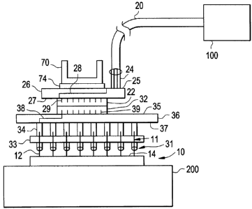
FIG. 4 illustrates one embodiment of the exemplary connector interfacing PCB
36
interfacing the cable terminating PCB surface mounted connectors 22 to the PGA
connector 10 of the second electronic device 200 via the connectors and
circuits on
the connector interfacing PCB 36. As illustrated, the pins 12 of the PGA
connector 10
of the second electronic device 200 are inserted into the sockets 34 of the
connector
interfacing PCB surface mounted socket grid array 33, which are connected to a
particular electrical contact of the connector interfacing PCB surface mounted
connector 32, which is mated with a particular electrical contact of the cable
terminating PCB surface mounted connector 22, which is connected to a
particular
conductor 24 from the multi-conductor cable 20, which extends from the first
electronic device 100. It can be seen from this assembly, that regardless of
what style
of connector is used for the second electronic device 200, the same (i.e.,
standardized)
multi-conductor cable 20 with the same cable terminating PCB surface mounted
connectors 22 can be used, since all that must be customized is the connector
interfacing PCB 36.
In order to maintain the connections between the various connectors and PCBs,
a
support device 70 (e.g., a clamp or bracket) can be used as shown in FIG. 4.
The
7
CA 02714539 2010-09-09
238491
support device 70 can be placed in position on top of each cable terminating
PCB
surface mounted connector 22 and fixed to a housing (not shown) or otherwise
held
firmly against each cable terminating PCB surface mounted connector 22. The
support device 70 can be made of metal, plastic, or any semi-rigid or rigid
material.
For example, aluminum can be used based on its light weight and malleability.
A pad
74 can be placed between the support device 70 and the top of each cable
terminating
PCB surface mounted connector 22. This pad 74 (e.g., a sponge, soft foam, or
other
cushioning material) can protect the electrical components from being damaged
by
contact or pressure against the bottom surface of the support device 70, which
can be
hard or abrasive.
This written description uses examples to disclose the invention, including
the best
mode, and also to enable any person skilled in the art to make and use the
invention.
The patentable scope of the invention is defined by the claims, and may
include other
examples that occur to those skilled in the art. Such other examples are
intended to be
within the scope of the claims if they have structural elements that do not
differ from
the literal language of the claims, or if they include equivalent structural
elements
with insubstantial differences from the literal language of the claims.
8