Note: Descriptions are shown in the official language in which they were submitted.
CA 02715274 2010-08-10
WO 2009/102637 PCT/US2009/033419
METHOD AND APPARATUS FOR SENSING, MEASUREMENT OR
CHARACTERIZATION OF DISPLAY ELEMENTS INTEGRATED WITH THE
DISPLAY DRIVE SCHEME, AND SYSTEM AND APPLICATIONS USING THE
SAME
CROSS REFERENCE TO RELATED APPLICATIONS
[0001] This application claims priority to U.S. Provisional Application No.
61/027727, filed on February 11, 2008, entitled "METHOD AND APPARATUS FOR
SENSING, MEASUREMENT OR CHARACTERIZATION OF DISPLAY ELEMENTS
INTEGRATED WITH THE DISPLAY DRIVE SCHEME, AND SYSTEM AND
APPLICATIONS USING THE SAME," the disclosure of which is hereby incorporated
by
reference in its entirety.
BACKGROUND
Field of the Invention
[0002] This invention relates to microelectromechanical systems. More
particularly, this invention relates to methods and apparatus for improving
the performance of
microelectromechanical systems such as interferometric modulators.
Description of the Related Art
[0003] Microelectromechanical systems (MEMS) include micro mechanical
elements, actuators, and electronics. Micromechanical elements may be created
using
deposition, etching, and/or other micromachining processes that etch away
parts of substrates
and/or deposited material layers or that add layers to form electrical and
electromechanical
devices. One type of MEMS device is called an interferometric modulator. As
used herein,
the term interferometric modulator or interferometric light modulator refers
to a device that
selectively absorbs and/or reflects light using the principles of optical
interference. In certain
embodiments, an interferometric modulator may comprise a pair of conductive
plates, one or
both of which may be transparent and/or reflective in whole or part and
capable of relative
motion upon application of an appropriate electrical signal. In a particular
embodiment, one
plate may comprise a stationary layer deposited on a substrate and the other
plate may
-1-
CA 02715274 2010-08-10
WO 2009/102637 PCT/US2009/033419
comprise a metallic membrane separated from the stationary layer by an air
gap. As
described herein in more detail, the position of one plate in relation to
another can change the
optical interference of light incident on the interferometric modulator. Such
devices have a
wide range of applications, and it would be beneficial in the art to utilize
and/or modify the
characteristics of these types of devices so that their features can be
exploited in improving
existing products and creating new products that have not yet been developed.
[0004] The systems, methods, and devices described herein each have several
aspects, no single one of which is solely responsible for its desirable
attributes. Without
limiting the scope, prominent features will now be discussed briefly. After
considering this
discussion, and particularly after reading the section entitled "Detailed
Description of Certain
Embodiments" one will understand how the features described herein provide
advantages
over other display devices.
SUMMARY
[0005] One aspect is a method, including applying a signal between a first
electrode and a second electrode of a display element, where the signal is at
a level which
results in the display element being in a first of a plurality of display
states, applying a second
signal between the two the electrodes to transition the display element from
one state to
another, measuring an electrical response of the display element in response
to the applied
second signal, identifying whether or not the display element reached the
desired final state
based upon the measured electrical response, and adjusting the second signal
if the display
element did not reach the desired final state.
[0006] Another aspect is an apparatus, including drive circuitry configured to
apply a signal between a first electrode and a second electrode of a display
element, where
the signal is at a level which results in the display element being in a first
of a plurality of
display states, feedback circuitry configured to measure an electrical
response of the display
element in response to the applied signal, and a processor configured control
the drive
circuitry, receive information indicative of the measured electrical response,
identify an error
in operation of the display element based upon the measured electrical
response, and adjust
the drive signal of the display element in response to the identified error.
-2-
CA 02715274 2010-08-10
WO 2009/102637 PCT/US2009/033419
[0007] Another aspect is a display device, including means for applying a
signal
between a first electrode and a second electrode of a display element, where
the signal is at a
level which results in the display element being in a first of a plurality of
display states,
means for measuring an electrical response of the display element in response
to the applied
signal, means for identifying an error in operation of the display element
based upon the
measured electrical response, and for adjusting the signal in response to the
identified error.
[0008] Another aspect is a display device including an array of
interferometric
modulators, drive circuitry configured to apply a signal between a first
electrode and a second
electrode of a display element, where the signal is at a level that results in
the display element
being in a first of a plurality of display states, feedback circuitry
configured to measure an
electrical response of the display element in response to the applied drive
voltage, a processor
configured control the drive circuitry, receive information indicative of the
measured
electrical response, identify an error in operation of the display element
based upon the
measured electrical response, and adjust the signal in response to the
identified error, and a
memory device configured to communicate with the processor.
BRIEF DESCRIPTION OF THE DRAWINGS
[0009] FIG. 1 is an isometric view depicting a portion of one embodiment of an
interferometric modulator display in which a movable reflective layer of a
first
interferometric modulator is in a relaxed position and a movable reflective
layer of a second
interferometric modulator is in an actuated position.
[0010] FIG. 2 is a system block diagram illustrating one embodiment of an
electronic device incorporating a 3x3 interferometric modulator display.
[0011] FIG. 3 is a diagram of movable mirror position versus applied voltage
for
one exemplary embodiment of an interferometric modulator of FIG. 1.
[0012] FIG. 4 is an illustration of a set of row and column voltages that may
be
used to drive an interferometric modulator display.
[0013] FIG. 5A illustrates one exemplary frame of display data in the 3x3
interferometric modulator display of FIG. 2.
-3-
CA 02715274 2010-08-10
WO 2009/102637 PCT/US2009/033419
[0014] FIG. 5B illustrates one exemplary timing diagram for row and column
signals that may be used to write the frame of FIG. 5A.
[0015] FIGS. 6A and 6B are system block diagrams illustrating an embodiment of
a visual display device comprising a plurality of interferometric modulators.
[0016] FIG. 7A is a cross section of the device of FIG. 1.
[0017] FIG. 7B is a cross section of an alternative embodiment of an
interferometric modulator.
[0018] FIG. 7C is a cross section of another alternative embodiment of an
interferometric modulator.
[0019] FIG. 7D is a cross section of yet another alternative embodiment of an
interferometric modulator.
[0020] FIG. 7E is a cross section of an additional alternative embodiment of
an
interferometric modulator.
[0021] FIG. 8 is a block diagram illustrating an example system configured to
drive a display array and measure an electrical response of selected display
elements, such as
the interferometric modulator display device of FIG. 2.
[0022] FIG. 9 is a block diagram illustrating another example of circuitry
that can
be used to measure an electrical response of selected display elements via the
same circuitry
used to apply a stimulus to the selected display elements, such as in the
interferometric
modulator display device of FIG. 2.
[0023] FIG. I OA is a flowchart illustrating an example of a method of driving
a
display element, such as, for example, the interferometric modulator as
illustrated in FIG. 1,
where a ramped drive voltage is used.
[0024] FIG. 10B is a flowchart illustrating a method of calibrating drive
voltages
for driving a display element including determining a drive voltage based on a
desired
operational characteristic of the display element.
[0025] FIG. IOC is a flowchart illustrating another method of calibrating
drive
voltages for driving a display element including adjusting a drive voltage
based on
identifying an error condition when driving the display element.
-4-
CA 02715274 2010-08-10
WO 2009/102637 PCT/US2009/033419
[0026] FIG. I IA is an illustration of an example of a ramped voltage waveform
for driving a display element.
[0027] Figure 11 B is an illustration of a sensed electrical response of drive
circuitry connected to the display element that may be used in the methods
illustrated in
FIGS. I OA and 1013.
[0028] FIG. 12 illustrates an example of a drive voltage waveform for driving
a
display element and a corresponding electrical response sensed in drive
circuitry connected to
the display element, such as may be used in the methods illustrated in FIGS. I
OA and 10B.
[0029] FIG. 13A illustrates an example of a drive voltage waveform and
corresponding electrical response indicative of proper actuation of a display
element, such as
may be used in the method illustrated in FIG. 10C.
[0030] FIG. 13B illustrates an example of a drive voltage waveform and
corresponding electrical response indicative of an example of erroneous
actuation of a display
element, such as may be used in the method illustrated in FIG. 10C.
[0031] FIG. 14 is a flowchart illustrating a method for driving a display
element
and measuring an electrical response of the display element to determine a
drive voltage to
achieve a desired operational characteristic, where the drive voltage results
in a display state
transition that is substantially undetectable to human vision.
[0032] FIG. 15 illustrates an example of a drive voltage waveform and
corresponding sensed electrical response that may be used in the method
illustrated in FIG.
15.
[0033] FIG. 16A is a block diagram illustrating an example of circuitry for
driving an isolated portion of a display array and for sensing an electrical
response of the
isolated area.
[0034] FIG. 16B illustrates an equivalent circuit illustrating the electrical
relationship of capacitance of a display area being sensed, and capacitances
of other display
areas not being sensed.
DETAILED DESCRIPTION
-5-
CA 02715274 2010-08-10
WO 2009/102637 PCT/US2009/033419
[0035] The following detailed description is directed to certain specific
embodiments. However, other embodiments may be used and some elements can be
embodied in a multitude of different ways. In this description, reference is
made to the
drawings wherein like parts are designated with like numerals throughout. As
will be
apparent from the following description, the embodiments may be implemented in
any device
that is configured to display an image, whether in motion (e.g., video) or
stationary (e.g., still
image), and whether textual or pictorial. More particularly, it is
contemplated that the
embodiments may be implemented in or associated with a variety of electronic
devices such
as, but not limited to, mobile telephones, wireless devices, personal data
assistants (PDAs),
hand-held or portable computers, GPS receivers/navigators, cameras, MP3
players,
camcorders, game consoles, wrist watches, clocks, calculators, television
monitors, flat panel
displays, computer monitors, auto displays (e.g., odometer display, etc.),
cockpit controls
and/or displays, display of camera views (e.g., display of a rear view camera
in a vehicle),
electronic photographs, electronic billboards or signs, projectors,
architectural structures,
packaging, and aesthetic structures (e.g., display of images on a piece of
jewelry). MEMS
devices of similar structure to those described herein can also be used in non-
display
applications such as in electronic switching devices.
[0036] Methods and systems for electrical sensing, measurement and
characterization of display elements are described. An embodiment includes
integrating the
electrical sensing, measurement and characterization with the display drive
scheme. This
embodiment allows for measurement of DC or operational hysteresis voltages
and/or
response times of interferometric modulator MEMS devices, for example, to be
fully
integrated with the display driver IC and/or the display drive scheme. Another
embodiment
allows these measurements to be performed and used without resulting in
display artifacts
visible to a human user. Another embodiment allows the measurement circuitry
to be
integrated with the display driver IC and/or the display drive scheme re-using
several existing
circuitry components and features, thus allowing for integration of the
measurement method
and its use relatively easily.
[0037] One interferometric modulator display embodiment comprising an
interferometric MEMS display element is illustrated in Figure 1. In these
devices, the pixels
-6-
CA 02715274 2010-08-10
WO 2009/102637 PCT/US2009/033419
are in either a bright or dark state. In the bright ("on" or "open") state,
the display element
reflects a large portion of incident visible light to a user. When in the dark
("off' or
"closed") state, the display element reflects little incident visible light to
the user. Depending
on the embodiment, the light reflectance properties of the "on" and "off'
states may be
reversed. MEMS pixels can be configured to reflect predominantly at selected
colors,
allowing for a color display in addition to black and white.
[0038] Figure 1 is an isometric view depicting two adjacent pixels in a series
of
pixels of a visual display, wherein each pixel comprises a MEMS
interferometric modulator.
In some embodiments, an interferometric modulator display comprises a
row/column array of
these interferometric modulators. Each interferometric modulator includes a
pair of
reflective layers positioned at a variable and controllable distance from each
other to form a
resonant optical gap with at least one variable dimension. In one embodiment,
one of the
reflective layers may be moved between two positions. In the first position,
referred to herein
as the relaxed position, the movable reflective layer is positioned at a
relatively large distance
from a fixed partially reflective layer. In the second position, referred to
herein as the
actuated position, the movable reflective layer is positioned more closely
adjacent to the
partially reflective layer. Incident light that reflects from the two layers
interferes
constructively or destructively depending on the position of the movable
reflective layer,
producing either an overall reflective or non-reflective state for each pixel.
[0039] The depicted portion of the pixel array in Figure 1 includes two
adjacent
interferometric modulators 12a and 12b. In the interferometric modulator 12a
on the left, a
movable reflective layer 14a is illustrated in a relaxed position at a
predetermined distance
from an optical stack 16a, which includes a partially reflective layer. In the
interferometric
modulator 12b on the right, the movable reflective layer 14b is illustrated in
an actuated
position adjacent to the optical stack 16b.
[0040] The optical stacks 16a and l6b (collectively referred to as optical
stack
16), as referenced herein, typically comprise several fused layers, which can
include an
electrode layer, such as indium tin oxide (ITO), a partially reflective layer,
such as chromium,
and a transparent dielectric. The optical stack 16 is thus electrically
conductive, partially
transparent, and partially reflective, and may be fabricated, for example, by
depositing one or
-7-
CA 02715274 2010-08-10
WO 2009/102637 PCT/US2009/033419
more of the above layers onto a transparent substrate 20. The partially
reflective layer can be
formed from a variety of materials that are partially reflective such as
various metals,
semiconductors, and dielectrics. The partially reflective layer can be formed
of one or more
layers of materials, and each of the layers can be formed of a single material
or a combination
of materials.
[0041] In some embodiments, the layers of the optical stack 16 are patterned
into
parallel strips, and may form row electrodes in a display device as described
further below.
The movable reflective layers 14a, l4b may be formed as a series of parallel
strips of a
deposited metal layer or layers (orthogonal to the row electrodes of 16a, 16b)
deposited on
top of posts 18 and an intervening sacrificial material deposited between the
posts 18. When
the sacrificial material is etched away, the movable reflective layers 14a,
14b are separated
from the optical stacks 16a, 16b by a defined gap 19. A highly conductive and
reflective
material such as aluminum may be used for the reflective layers 14, and these
strips may form
column electrodes in a display device.
[0042] With no applied voltage, the gap 19 remains between the movable
reflective layer 14a and optical stack 16a, with the movable reflective layer
14a in a
mechanically relaxed state, as illustrated by the pixel 12a in Figure 1.
However, when a
potential difference is applied to a selected row and column, the capacitor
formed at the
intersection of the row and column electrodes at the corresponding pixel
becomes charged,
and electrostatic forces pull the electrodes together. If the voltage is high
enough, the
movable reflective layer 14 is deformed and is forced against the optical
stack 16. A
dielectric layer (not illustrated in this Figure) within the optical stack 16
may prevent shorting
and control the separation distance between layers 14 and 16, as illustrated
by pixel 12b on
the right in Figure 1. The behavior is the same regardless of the polarity of
the applied
potential difference. In this way, row/column actuation that can control the
reflective vs.
non-reflective pixel states is analogous in many ways to that used in
conventional LCD and
other display technologies.
[0043] Figures 2 through 5B illustrate one exemplary process and system for
using an array of interferometric modulators in a display application.
-8-
CA 02715274 2010-08-10
WO 2009/102637 PCT/US2009/033419
100441 Figure 2 is a system block diagram illustrating one embodiment of an
electronic device that may incorporate aspects of the invention. In the
exemplary
embodiment, the electronic device includes a processor 21 which may be any
general purpose
single- or multi-chip microprocessor such as an ARM, Pentium , Pentium 11 ,
Pentium III ,
Pentium IV , Pentium Pro, an 8051, a MIPS , a Power PC , an ALPHA , or any
special
purpose microprocessor such as a digital signal processor, microcontroller, or
a
programmable gate array. As is conventional in the art, the processor 21 may
be configured
to execute one or more software modules. In addition to executing an operating
system, the
processor may be configured to execute one or more software applications,
including a web
browser, a telephone application, an email program, or any other software
application.
[00451 In one embodiment, the processor 21 is also configured to communicate
with an array driver 22. In one embodiment, the array driver 22 includes a row
driver circuit
24 and a column driver circuit 26 that provide signals to a display array or
panel 30. The
cross section of the array illustrated in Figure 1 is shown by the lines 1-1
in Figure 2. For
MEMS interferometric modulators, the row/column actuation protocol may take
advantage of
a hysteresis property of these devices illustrated in Figure 3. It may
require, for example, a
volt potential difference to cause a movable layer to deform from the relaxed
state to the
actuated state. However, when the voltage is reduced from that value, the
movable layer
maintains its state as the voltage drops back below 10 volts. In the exemplary
embodiment of
Figure 3, the movable layer does not relax completely until the voltage drops
below 2 volts.
Thus, there exists a window of applied voltage, about 3 to 7 V in the example
illustrated in
Figure 3, within which the device is stable in either the relaxed or actuated
state. This is
referred to herein as the "hysteresis window" or "stability window." For a
display array
having the hysteresis characteristics of Figure 3, the row/column actuation
protocol can be
designed such that during row strobing, pixels in the strobed row that are to
be actuated are
exposed to a voltage difference of about 10 volts, and pixels that are to be
relaxed are
exposed to a voltage difference of close to zero volts. After the strobe, the
pixels are exposed
to a steady state voltage difference of about 5 volts such that they remain in
whatever state
the row strobe put them in. After being written, each pixel sees a potential
difference within
the "stability window" of 3-7 volts in this example. This feature makes the
pixel design
-9-
CA 02715274 2010-08-10
WO 2009/102637 PCT/US2009/033419
illustrated in Figure 1 stable under the same applied voltage conditions in
either an actuated
or relaxed pre-existing state. Since each pixel of the interferometric
modulator, whether in
the actuated or relaxed state, is essentially a capacitor formed by the fixed
and moving
reflective layers, this stable state can be held at a voltage within the
hysteresis window with
almost no power dissipation. Essentially no current flows into the pixel if
the applied
potential is fixed.
[00461 In typical applications, a display frame may be created by asserting
the set
of column electrodes in accordance with the desired set of actuated pixels in
the first row. A
row pulse is then applied to the row 1 electrode, actuating the pixels
corresponding to the
asserted column lines. The asserted set of column electrodes is then changed
to correspond
to the desired set of actuated pixels in the second row. A pulse is then
applied to the row 2
electrode, actuating the appropriate pixels in row 2 in accordance with the
asserted column
electrodes. The row 1 pixels are unaffected by the row 2 pulse, and remain in
the state they
were set to during the row 1 pulse. This may be repeated for the entire series
of rows in a
sequential fashion to produce the frame. Generally, the frames are refreshed
and/or updated
with new display data by continually repeating this process at some desired
number of frames
per second. A wide variety of protocols for driving row and column electrodes
of pixel
arrays to produce display frames are also well known and may be used in
conjunction with
the present invention.
[00471 Figures 4, 5A, and 5B illustrate one possible actuation protocol for
creating a display frame on the 3x3 array of Figure 2. Figure 4 illustrates a
possible set of
column and row voltage levels that may be used for pixels exhibiting the
hysteresis curves of
Figure 3. In the Figure 4 embodiment, actuating a pixel involves setting the
appropriate
column to -Vbias, and the appropriate row to +AV, which may correspond to -5
volts and +5
volts, respectively. Relaxing the pixel is accomplished by setting the
appropriate column to
+Vb;as, and the appropriate row to the same +AV, producing a zero volt
potential difference
across the pixel. In those rows where the row voltage is held at zero volts,
the pixels are
stable in whatever state they were originally in, regardless of whether the
column is at +Vb;as,
or -Vbias= As is also illustrated in Figure 4, it will be appreciated that
voltages of opposite
polarity than those described above can be used, e.g., actuating a pixel can
involve setting the
-10-
CA 02715274 2010-08-10
WO 2009/102637 PCT/US2009/033419
appropriate column to +Vbias, and the appropriate row to -AV. In this
embodiment, releasing
the pixel is accomplished by setting the appropriate column to -Vbias, and the
appropriate row
to the same -AV, producing a zero volt potential difference across the pixel.
[0048] Figure 5B is a timing diagram showing a series of row and column
signals
applied to the 3x3 array of Figure 2 which will result in the display
arrangement illustrated in
Figure 5A, where actuated pixels are non-reflective. Prior to writing the
frame illustrated in
Figure 5A, the pixels can be in any state, and in this example, all the rows
are at 0 volts, and
all the columns are at +5 volts. With these applied voltages, all pixels are
stable in their
existing actuated or relaxed states.
[0049] In the Figure 5A frame, pixels (1,1), (1,2), (2,2), (3,2) and (3,3) are
actuated. To accomplish this, during a "line time" for row 1, columns 1 and 2
are set to -5
volts, and column 3 is set to +5 volts. This does not change the state of any
pixels, because
all the pixels remain in the 3-7 volt stability window. Row 1 is then strobed
with a pulse that
goes from 0, up to 5 volts, and back to zero. This actuates the (1,1) and
(1,2) pixels and
relaxes the (1,3) pixel. No other pixels in the array are affected. To set row
2 as desired,
column 2 is set to -5 volts, and columns 1 and 3 are set to +5 volts. The same
strobe applied
to row 2 will then actuate pixel (2,2) and relax pixels (2,1) and (2,3).
Again, no other pixels
of the array are affected. Row 3 is similarly set by setting columns 2 and 3
to -5 volts, and
column l to +5 volts. The row 3 strobe sets the row 3 pixels as shown in
Figure 5A. After
writing the frame, the row potentials are zero, and the column potentials can
remain at either
+5 or -5 volts, and the display is then stable in the arrangement of Figure
5A. It will be
appreciated that the same procedure can be employed for arrays of dozens or
hundreds of
rows and columns. It will also be appreciated that the timing, sequence, and
levels of
voltages used to perform row and column actuation can be varied widely within
the general
principles outlined above, and the above example is exemplary only, and any
actuation
voltage method can be used with the systems and methods described herein.
[0050] Figures 6A and 6B are system block diagrams illustrating an embodiment
of a display device 40. The display device 40 can be, for example, a cellular
or mobile
telephone. However, the same components of display device 40 or slight
variations thereof
-11-
CA 02715274 2010-08-10
WO 2009/102637 PCT/US2009/033419
are also illustrative of various types of display devices such as televisions
and portable media
players.
[0051] The display device 40 includes a housing 41, a display 30, an antenna
43, a
speaker 45, an input device 48, and a microphone 46. The housing 41 is
generally formed
from any of a variety of manufacturing processes as are well known to those of
skill in the
art, including injection molding and vacuum forming. In addition, the housing
41 may be
made from any of a variety of materials, including, but not limited to,
plastic, metal, glass,
rubber, and ceramic, or a combination thereof. In one embodiment, the housing
41 includes
removable portions (not shown) that may be interchanged with other removable
portions of
different color, or containing different logos, pictures, or symbols.
[0052] The display 30 of exemplary display device 40 may be any of a variety
of
displays, including a bi-stable display, as described herein. In other
embodiments, the display
30 includes a flat-panel display, such as plasma, EL, OLED, STN LCD, or TFT
LCD as
described above, or a non-flat-panel display, such as a CRT or other tube
device, as is well
known to those of skill in the art. However, for purposes of describing the
present
embodiment, the display 30 includes an interferometric modulator display, as
described
herein.
[0053] The components of one embodiment of exemplary display device 40 are
schematically illustrated in Figure 6B. The illustrated exemplary display
device 40 includes a
housing 41 and can include additional components at least partially enclosed
therein. For
example, in one embodiment, the exemplary display device 40 includes a network
interface
27 that includes an antenna 43, which is coupled to a transceiver 47. The
transceiver 47 is
connected to a processor 21, which is connected to conditioning hardware 52.
The
conditioning hardware 52 may be configured to condition a signal (e.g., filter
a signal). The
conditioning hardware 52 is connected to a speaker 45 and a microphone 46. The
processor
21 is also connected to an input device 48 and a driver controller 29. The
driver controller 29
is coupled to a frame buffer 28 and to an array driver 22, which in turn is
coupled to a display
array 30. A power supply 50 provides power to all components as required by
the particular
exemplary display device 40 design.
-12-
CA 02715274 2010-08-10
WO 2009/102637 PCT/US2009/033419
[0054] The network interface 27 includes the antenna 43 and the transceiver 47
so
that the exemplary display device 40 can communicate with one or more devices
over a
network. In one embodiment, the network interface 27 may also have some
processing
capabilities to relieve requirements of the processor 21. The antenna 43 is
any antenna
known to those of skill in the art for transmitting and receiving signals. In
one embodiment,
the antenna transmits and receives RF signals according to the IEEE 802.11
standard,
including IEEE 802.11(a), (b), or (g). In another embodiment, the antenna
transmits and
receives RF signals according to the BLUETOOTH standard. In the case of a
cellular
telephone, the antenna is designed to receive CDMA, GSM, AMPS, or other known
signals
that are used to communicate within a wireless cell phone network. The
transceiver 47 pre-
processes the signals received from the antenna 43 so that they may be
received by and
further manipulated by the processor 21. The transceiver 47 also processes
signals received
from the processor 21 so that they may be transmitted from the exemplary
display device 40
via the antenna 43.
[0055] In an alternative embodiment, the transceiver 47 can be replaced by a
receiver. In yet another alternative embodiment, network interface 27 can be
replaced by an
image source, which can store or generate image data to be sent to the
processor 21. For
example, the image source can be a digital video disc (DVD) or a hard-disc
drive that
contains image data, or a software module that generates image data.
[0056] Processor 21 generally controls the overall operation of the exemplary
display device 40. The processor 21 receives data, such as compressed image
data from the
network interface 27 or an image source, and processes the data into raw image
data or into a
format that is readily processed into raw image data. The processor 21 then
sends the
processed data to the driver controller 29 or to frame buffer 28 for storage.
Raw data
typically refers to the information that identifies the image characteristics
at each location
within an image. For example, such image characteristics can include color,
saturation, and
gray-scale level.
[0057) In one embodiment, the processor 21 includes a microcontroller, CPU, or
logic unit to control operation of the exemplary display device 40.
Conditioning hardware 52
generally includes amplifiers and filters for transmitting signals to the
speaker 45, and for
-13-
CA 02715274 2010-08-10
WO 2009/102637 PCT/US2009/033419
receiving signals from the microphone 46. Conditioning hardware 52 may be
discrete
components within the exemplary display device 40, or may be incorporated
within the
processor 21 or other components.
[0058] The driver controller 29 takes the raw image data generated by the
processor 21 either directly from the processor 21 or from the frame buffer 28
and reformats
the raw image data appropriately for high speed transmission to the array
driver 22.
Specifically, the driver controller 29 reformats the raw image data into a
data flow having a
raster-like format, such that it has a time order suitable for scanning across
the display array
30. Then the driver controller 29 sends the formatted information to the array
driver 22.
Although a driver controller 29, such as a LCD controller, is often associated
with the system
processor 21 as a stand-alone Integrated Circuit (IC), such controllers may be
implemented in
many ways. They may be embedded in the processor 21 as hardware, embedded in
the
processor 21 as software, or fully integrated in hardware with the array
driver 22.
[0059] Typically, the array driver 22 receives the formatted information from
the
driver controller 29 and reformats the video data into a parallel set of
waveforms that are
applied many times per second to the hundreds and sometimes thousands of leads
coming
from the display's x-y matrix of pixels.
[0060] In one embodiment, the driver controller 29, array driver 22, and
display
array 30 are appropriate for any of the types of displays described herein.
For example, in
one embodiment, driver controller 29 is a conventional display controller or a
bi-stable
display controller (e.g., an interferometric modulator controller). In another
embodiment,
array driver 22 is a conventional driver or a bi-stable display driver (e.g.,
an interferometric
modulator display). In one embodiment, a driver controller 29 is integrated
with the array
driver 22. Such an embodiment is common in highly integrated systems such as
cellular
phones, watches, and other small area displays. In yet another embodiment,
display array 30
is a typical display array or a bi-stable display array (e.g., a display
including an array of
interferometric modulators).
[0061] The input device 48 allows a user to control the operation of the
exemplary display device 40. In one embodiment, input device 48 includes a
keypad, such as
a QWERTY keyboard or a telephone keypad, a button, a switch, a touch-sensitive
screen, or a
-14-
CA 02715274 2010-08-10
WO 2009/102637 PCT/US2009/033419
pressure- or heat-sensitive membrane. In one embodiment, the microphone 46 is
an input
device for the exemplary display device 40. When the microphone 46 is used to
input data to
the device, voice commands may be provided by a user for controlling
operations of the
exemplary display device 40.
[00621 Power supply 50 can include a variety of energy storage devices as are
well known in the art. For example, in one embodiment, power supply 50 is a
rechargeable
battery, such as a nickel-cadmium battery or a lithium ion battery. In another
embodiment,
power supply 50 is a renewable energy source, a capacitor, or a solar cell
including a plastic
solar cell, and solar-cell paint. In another embodiment, power supply 50 is
configured to
receive power from a wall outlet.
[00631 In some embodiments, control programmability resides, as described
above, in a driver controller which can be located in several places in the
electronic display
system. In some embodiments, control programmability resides in the array
driver 22 Those
of skill in the art will recognize that the above-described optimizations may
be implemented
in any number of hardware and/or software components and in various
configurations.
[00641 The details of the structure of interferometric modulators that operate
in
accordance with the principles set forth above may vary widely. For example,
Figures 7A-7E
illustrate five different embodiments of the movable reflective layer 14 and
its supporting
structures. Figure 7A is a cross section of the embodiment of Figure 1, where
a strip of metal
material 14 is deposited on orthogonally extending supports 18. In Figure 7B,
the moveable
reflective layer 14 is attached to supports at the corners only, on tethers
32. In Figure 7C, the
moveable reflective layer 14 is suspended from a deformable layer 34, which
may comprise a
flexible metal. The deformable layer 34 connects, directly or indirectly, to
the substrate 20
around the perimeter of the deformable layer 34. These connections are herein
referred to as
support posts. The embodiment illustrated in Figure 7D has support post plugs
42 upon
which the deformable layer 34 rests. The movable reflective layer 14 remains
suspended
over the gap, as in Figures 7A-7C, but the deformable layer 34 does not form
the support
posts by filling holes between the deformable layer 34 and the optical stack
16. Rather, the
support posts are formed of a planarization material, which is used to form
support post plugs
42. The embodiment illustrated in Figure 7E is based on the embodiment shown
in Figure
-15-
CA 02715274 2010-08-10
WO 2009/102637 PCT/US2009/033419
7D, but may also be adapted to work with any of the embodiments illustrated in
Figures 7A-
7C, as well as additional embodiments not shown. In the embodiment shown in
Figure 7E,
an extra layer of metal or other conductive material has been used to form a
bus structure 44.
This allows signal routing along the back of the interferometric modulators,
eliminating a
number of electrodes that may otherwise have had to be formed on the substrate
20.
[0065] In embodiments such as those shown in Figure 7, the interferometric
modulators function as direct-view devices, in which images are viewed from
the front side
of the transparent substrate 20, the side opposite to that upon which the
modulator is
arranged. In these embodiments, the reflective layer 14 optically shields the
portions of the
interferometric modulator on the side of the reflective layer opposite the
substrate 20,
including the deformable layer 34. This allows the shielded areas to be
configured and
operated upon without negatively affecting the image quality. Such shielding
allows the bus
structure 44 in Figure 7E, which provides the ability to separate the optical
properties of the
modulator from the electromechanical properties of the modulator, such as
addressing and the
movements that result from that addressing. This separable modulator
architecture allows the
structural design and materials used for the electromechanical aspects and the
optical aspects
of the modulator to be selected and to function independently of each other.
Moreover, the
embodiments shown in Figures 7C-7E have additional benefits deriving from the
decoupling
of the optical properties of the reflective layer 14 from its mechanical
properties, which are
carried out by the deformable layer 34. This allows the structural design and
materials used
for the reflective layer 14 to be optimized with respect to the optical
properties, and the
structural design and materials used for the deformable layer 34 to be
optimized with respect
to desired mechanical properties.
[0066] The following description is directed to methods and devices used to
provide, monitor and adapt drive voltages of a wide variety of MEMS elements,
such as
MEMS switches, and other elements having deflected or deformed electrodes
and/or mirrors.
Although the specific examples discussed use interferometric modulators as the
elements, the
principles discussed may apply to other MEMS elements as well.
[0067] Display devices like those based on interferometric modulator
technology
may be measured and characterized electronically and/or mechanically.
Depending on the
-16-
CA 02715274 2010-08-10
WO 2009/102637 PCT/US2009/033419
display technology, these measurements can form a part of calibration of the
display module
(the display "module" referred to herein includes the display panel, the
display driver, and
associated components such as cabling, etc.), and the measurement parameters
may be stored
into a non-volatile memory (e.g., NVRAM) in the display module for future use.
As
discussed above with reference to Figure 3, the interferometric modulators
operate based on a
potential difference applied to them. Figure 3 shows that the interferometric
modulators are
in either the relaxed (or released) state or in the actuated state, depending
on the magnitude of
the potential difference applied between their electrodes. As shown, the
changing of one
state to another happens according to a hysteretic characteristic with a
stability (or hold)
window, where the device holds its current state when the applied potential
difference falls
within the hold window. As used herein, a "bias voltage" refers to a potential
difference that
falls within the hold window. Accordingly, as shown in Figure 3, there are
five input voltage
difference ranges in some embodiments. Each of the five voltage difference
ranges has a title
reflecting its effect on the state of the interferometric modulator. Starting
from the left of
Figure 3, the five voltage difference ranges are: 1) negative actuate
("Actuated"); 2) negative
hold ("Stability Window"); 3) release ("Relaxed"); 4) positive hold
("Stability Window");
and 5) positive actuate ("Actuated").
[0068] Based on theoretical understanding of the devices and past experimental
results, approximate values of the thresholds between these input voltage
difference ranges
may be known, but in order to more optimally operate the interferometric
modulator array,
the threshold voltages can be measured with more precision. For example, as
described
further herein, the thresholds may vary from device to device, lot to lot,
over temperature,
and/or as the device ages. Threshold values may accordingly be measured for
each
manufactured device or group of devices. One method of measuring the threshold
voltages is
to apply inputs of various voltage differences while monitoring the state of
the
interferometric modulators through observation of the optical characteristics
of the
interferometric modulators. This may be accomplished, for example, through
human
observation or by use of an optical measurement device. Additionally or
alternatively, the
state of the interferometric modulators may be monitored through electronic
response
measurement. In some embodiments, the array driver 22 of the display array 30,
discussed
-17-
CA 02715274 2010-08-10
WO 2009/102637 PCT/US2009/033419
above, may be configured to measure electrical responses of display elements
in order to
determine the state and/or operational characteristics of the display elements
according to the
methods discussed below.
(0069] Often times, the behavior of a display device changes with the age of
the
display device, with variations in temperature of the display, with the
content of the images
being displayed, etc. Display devices may have one or more electrical
parameters that change
in relation to the optical response or optical state. As discussed above, the
interferometric
modulator is set to an actuated state when the electrostatic attraction
between the reflective
layer and the optical stack is great enough to overcome the mechanical
restorative forces
working to hold the reflective layer in the relaxed state. Because the
reflective layer, the
optical stack, and the gap between them form two conductive plates separated
by a dielectric,
the structure has a capacitance. Also, because the capacitance of the
structure varies
according to the distance between the two plates, the capacitance of the
structure varies
according to the state of the interferometric modulator. Therefore, an
indication of the
capacitance can be used to determine the state of the interferometric
modulator.
[0070] In one aspect, an indication of the capacitance can be obtained, for
example, by sensing the current or charge used to change the voltage applied
between the
reflective layer and the optical stack. A relatively high amount of current or
charge indicates
that the capacitance is relatively large. Similarly, a relatively low amount
of current or charge
indicates that the capacitance is relatively small. The sensing of current or
charge may be
accomplished, for example through analog or digital integration of a signal
representing the
charge or current.
[0071] Similar characteristics can apply to LCD display technology where the
capacitance of the device is related to the resulting optical brightness of
the cell at a certain
temperature. In addition to the operational characteristics of display element
possibly
changing with age, the operational characteristics can be affected by the
temperature of the
display elements. The temperature of a display element can depend on the past
optical
response states that were displayed, and, thus, the operational
characteristics could vary
independently for each display element in the display array of the display
device.
-18-
CA 02715274 2010-08-10
WO 2009/102637 PCT/US2009/033419
[0072] In one embodiment, the relevant characteristics of the display device,
like
hysteresis voltages and response times for interferometric modulator MEMS
devices and
brightness-voltage relationship for LCD devices, are measured after
manufacturing at the
factory during a calibration procedure. This information can then be stored in
a memory the
display module used for driving the display device. Since the characteristics
of the display
device may also change with temperature and aging, for example, the effects of
temperature
and aging on these characteristics (e.g., temperature coefficient) may be
studied, measured
and also hardwired or stored in the memory of the display module. In spite of
this post-
manufacturing characterization, however, the calibration margins built into
the display device
may not allow for unpredictable changes in the characteristics of the display
device. In some
cases, the lifetime and quality of a display device may be improved by
performing
recalibration of the device after a certain period of use (e.g., one year), on
a random length
periodic basis, based on changes in temperature, etc. In other cases, the
drive scheme may be
robust enough to compensate for changes in characteristics of the display
device without such
recalibration. Examples of such recalibration and robust drive schemes are
discussed below.
[0073] Figure 8 is a block diagram illustrating an example system 100
configured
to drive a display array 102 and measure an electrical response of selected
display elements,
such as the interferometric modulators 12a and 12b of Figure 1. The display
array 102
comprises m columns by n rows of N-component pixels (e.g., N may be 3 display
elements
including red, green and blue, for example). The system 100 further includes a
column driver
comprising 2 or more digital to analog converters (DACs) 104 for supplying two
or more
drive voltage levels as well as a column switch subsystem 106 for selecting
the columns to
which data signals are supplied. The system 100 further includes a row driver
circuit
comprising two or more DACs 108 for supplying two or more drive voltage levels
as well as
a row switch circuit 110 for selecting which row to strobe. Note that the row
and column
drivers that are directly connected to the display array in this schematic are
shown as
composed of switches, but several methods discussed below are applicable to
alternative
driver designs including a full analog display driver. Note that while drive
voltages are
discussed herein, other drive signals, such as drive currents or drive charges
may be used.
-19-
CA 02715274 2010-08-10
WO 2009/102637 PCT/US2009/033419
[0074] The row and column driver circuitry including the DACs 104 and 108 and
the switches 106 and 110 are controlled by digital logic of an array driver
112. As discussed
above in reference to Figures 2 and 3, the row/column actuation protocol
contained in the
digital logic of the array driver 112 may take advantage of a hysteresis
property of
interferometric modulator MEMS devices. For example, in a display array
comprising
interferometric modulators 12 having the hysteresis characteristics of Figure
3, the
row/column actuation protocol can be designed such that during row strobing,
display
elements in the strobed row that are to be actuated are exposed to an
actuation voltage
difference (e.g., about 10 volts), and display elements that are to be relaxed
are exposed to a
voltage difference of close to zero volts, as shown in FIGs. 4 to 5. After the
strobe, the
display elements are exposed to a steady state voltage difference known as the
bias voltage
(e.g., about 5 volts) such that they remain in whatever state the row strobe
last put them.
After being written, each display element sees a potential difference within
the "stability
window" of 3-7 volts in this example. However, as discussed above, the
characteristics of
the display elements may change with time and/or temperature or may respond
more quickly
or slowly to different drive voltage levels. As such, the array driver 112 and
the DACs 104
and 108 may be configured to supply variable voltage levels, depending on the
embodiment.
[0075] In addition to the drive circuitry discussed above (including the DACs
104
and 108 and the switches 106 and 110, and the array driver 112), the remaining
blocks of the
system 100 are able to apply further electrical stimulus to selected display
elements, as well
as to be able to measure the electrical response of selected display elements
in the display
array 102. In this example, digital-to-analog converters (DACs) 114 and 116
supply
additional voltages to the display array 102 via the column and row switches
106 and 110,
respectively. In general, these may represent internal or external voltage
supply inputs to the
row and column drive circuitry.
[0076] In this example, a direct-digital-synthesis (DDS 1) block 118 is used
to
generate the electrical voltage stimulus that is added on the top of the
voltage level produced
by the DAC 114 connected to the column switch 106. The stimulus signal
produced by the
DDS I block 118 may be produced by several alternative means such as an
electrical
oscillator, a saw-tooth waveform generator, etc. which are familiar to those
skilled in the art.
-20-
CA 02715274 2010-08-10
WO 2009/102637 PCT/US2009/033419
In various embodiments, the stimulus may be current or charge, or even a
controlled output
impedance.
[0077] In the example shown in Figure 8, the electrical response of the
display
array 102 is measured in the form of electrical current flowing through the
display array 102
resulting from application of the electrical voltage stimulus to the row
and/or column
electrodes via the row and/or column switches 106 and 110, respectively. Other
forms of
measured electrical response can include voltage variations, etc. A trans-
impedance
amplifier 120 (shown in Figure 8 as a resistor 120A followed by an amplifier
120B) may be
used to measure the electrical response. The display element(s) for which the
measured
electrical response corresponds depends on the states of the column and row
switches 106
and 110. In alternative embodiments, analog, digital, or mixed-signal
processing may be
used for the purpose of measurement of the electrical response of the display
array 102.
[0078] In one embodiment, the electrical response of a display element is
measured directly by measuring the current through the input terminals of the
trans-
impedance amplifier 120. In this embodiment, the profile and/or peak values,
or other
characteristics known to skilled technologists, can be used to identify
certain operational
characteristics of the display element.
[0079] In another embodiment, operational characteristics of the display
element
being measured can be characterized by additional post processing of the
electrical response
output from the trans-impedance amplifier 120. An example of using post
processing
techniques to characterize the capacitance and the resistive component of the
impedance of
an interferometric modulator using the circuitry of Figure 8 is now discussed.
[0080] Since an interferometric modulator can be considered a capacitor, a
periodic stimulus, such as that which could be applied using the DDS 1 118,
will result in a
periodic output electrical response with a 90 phase lag. For example, the DDS
1 118 could
apply a sinusoidal voltage waveform, sin(wt), to the column electrode of the
display element.
For an ideal capacitor, the electrical response of the display element would
be a time
derivative of the applied stimulus, or cos(wt). Thus, the output of the trans-
impedance
amplifier 120 would also be a cosine function. A second DDS, DDS2 122, applies
a cosine
voltage waveform that is multiplied by the output of the trans-impedance
amplifier 120 at
-21-
CA 02715274 2010-08-10
WO 2009/102637 PCT/US2009/033419
multiplier 124. The result is a waveform with a constant component and a
periodic
component. The constant component of the output of the multiplier 124 is
proportional to the
capacitance of the display element. A filter 126 is used to filter out the
periodic component
and result in an electrical signal that is used to characterize the
capacitance, and therefore the
actuated or unactuated state, of the display element.
[0081] For a display element that is an ideal capacitor, the output of the
trans-
impedance amplifier 120 is a pure cosine function for the example where the
applied stimulus
is a sine function. However, if the display element exhibits any non-
capacitive impedance,
due to leakage for example, the output of the trans-impedance amplifier 120
will also contain
a sine component. This sine component does not affect the measurement of the
capacitance,
since it will be filtered out by the filter 126. The sine component can be
detected and used to
characterize the resistive portion of the impedance of the display element.
[0082] A periodic voltage waveform similar to the stimulus applied by the
DDS1,
sin(wt) for example, is multiplied by the output of the trans-impedance
amplifier 120 at a
multiplier 128. The result is an electrical response that includes a constant
component and a
periodic component. The constant component is proportional to the resistive
portion of the
impedance of the display element being measured. A filter 130 is used to
remove the
periodic component resulting in a signal that can be used to characterize the
resistive portion
of the impedance of the display element.
[0083] The outputs of the filters are converted to the digital domain by use
of a
dual analog to digital converter (ADC) 132. The output of the dual ADC 132 is
received by
the array driver 112 for use in carrying out the methods discussed below.
[0084] In the example circuitry shown in Figure 8, the characterization
stimulus is
applied to a column electrode and the electrical response is measured via a
row electrode. In
other embodiments, the electrical response can be measured from the same
electrode, row or
column, for example, to which the stimulus is applied. Figure 9 is a block
diagram
illustrating an example of circuitry 150 that can be used to measure an
electrical response of
selected display elements via the same circuitry used to apply a stimulus to
the selected
display elements, such as in the interferometric modulator display device of
Figure 2. The
circuit 150 comprises transistors Ni and P 1 which mirror the current from the
current source
-22-
CA 02715274 2010-08-10
WO 2009/102637 PCT/US2009/033419
transistors N2 and P2 used to drive the Vot,t signal applied to the display
element.
Accordingly, the current Iout is substantially equal to the current used for
driving the Vout
signal. Measuring the electrical response of the Ioõt signal may, therefore,
be used to
determine operational characteristics of the interferometric modulators such
as whether the
interferometric modulators are in a high or low capacitance state. Other
circuits may also be
used. The circuit 150 shown in Figure 9 is applicable to alternative driver IC
designs or drive
schemes for supplying a voltage waveform VoUt. The circuit 150 depicted in the
schematic of
Figure 9 can be used in current conveyor circuits and in current feedback
amplifiers, and can
apply an electrical voltage stimulus to the display array area and
simultaneously replicate the
current (response) to a different pin (Iout) for purposes of electrical
sensing.
[0085] There are several ways in which measured electrical responses, such as
those sensed by the systems shown in Figures 8 and 9, can be used as a
feedback signal to
affect the operation of the display driver circuitry. For example, the
measured information
may be analyzed in the digital domain, e.g., using the digital logic of array
driver 112 and/or
a processor configured to control the array driver 112 (e.g., the processor 21
and array driver
22 shown in Figure 2) and then used to adaptively drive the display array 102.
The measured
electrical responses may also be used to complete a feedback loop in the
analog domain (e.g.,
using the outputs of the DACs 104, 114, 108 and/or 116, or using the output of
the DDS1 118
shown in Figure 8). Examples of methods of driving interferometric modulator
display
elements using measured electrical responses as feedback are illustrated in
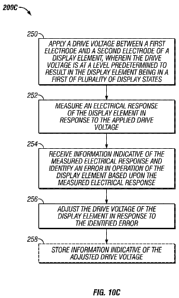
Figures 10A-1 OC.
[0086] Figure 10A is a flowchart illustrating an example of a method 200A of
driving a display element, such as, for example, the interferometric modulator
as illustrated in
Figure 1, where a ramped drive voltage is used. In one embodiment, the method
200A can be
performed by the array driver 112 for controlling the drive circuitry (e.g.,
the DACs 104, 108
and 114, the switches 106 and 110, and the DDS 1 118) shown in Figure 8 to
display images
on the display array 102. In other embodiments, a processor such as the
processor 21 in
Figure 2, can perform the method 200A. The method 200A provides a method of
adapting
drive voltage levels by applying a gradually increasing or decreasing voltage
waveform to a
display element and discontinuing the application of the voltage waveform when
a change in
state of the display element is sensed. In this way, the applied voltages,
including drive
-23-
CA 02715274 2010-08-10
WO 2009/102637 PCT/US2009/033419
voltages to actuate or release the display element, can be changed only as
much as necessary,
thereby conserving power.
[0087] The method 200A starts at block 202 where the array driver 112 applies
a
drive voltage between a first electrode and a second electrode of a display
element. The first
electrode may be one of the movable reflective layers (column electrodes) 14
and the second
electrode may be one of the row electrodes 16 of the interferometric
modulators 12 illustrated
in Figure 1. The drive voltage applied at block 202 may be a voltage at the
bias voltage
within the hysteresis window (e.g., 3-7 volts as discussed above), or,
alternatively may be a
static voltage level outside of the hysteresis window. As used herein, a
static voltage is a
voltage that is non-varying over time, such as over an actuation period. The
static drive
voltage difference applied to the two electrodes at block 202 may be supplied
by one or more
of the DACs 104 or 108 (FIG. 8) to the column and/or row electrodes,
respectively.
[0088] After the initial drive voltage is applied at the block 202, the method
200A
continues at block 204, where the array driver 112 ramps the level of the
drive voltage from a
first level (e.g., the static voltage level applied at block 202) to a second
level. Figure 1 IA is
an illustration of an example of a ramped voltage waveform for driving a
display element that
may be used in the method 200A. In Figure 11A, the initial drive voltage
applied at the block
202 is a 5 volt bias voltage 302 (the static voltage applied in block 202). At
approximately 2
ms, a ramped voltage waveform 304 is applied at block 204 in the method 200A.
The
ramped voltage waveform 304 continues to be increased until a measured
electrical response,
as sensed by electrical sensing feedback circuitry such as the trans-impedance
amplifier 120
in Figure 8, monitors an electrical response of the display element at block
206. For
example, the trans-impedance amplifier 120 may sense a change in the current
to or from the
display element, indicating a change in state of the display element.
[0089] In this example, the monitored electrical response is indicative of a
change
of state of the interferometric modulators 12 of Figure 1. Figure 11 B is an
illustration of a
sensed electrical response that may be sensed with the electrical sensing
feedback circuitry
connected to the drive circuitry of the display element using the method 200A
illustrated in
Figure 10A. At about 4 ms, the sensed electrical current shows a sharp rise
306 to a level of
about +5 milliamps. The sensitivity of the amplifier to the sensed electrical
current can
-24-
CA 02715274 2010-08-10
WO 2009/102637 PCT/US2009/033419
depend on the resistance of the circuitry being used for sensing. For example,
in an
embodiment such as that shown in Figure 8, the resistance of the resistor 120A
may be
chosen to result in a output amplitude that is easily measurable, depending on
the feedback
circuitry. Upon detecting the rise 306 in the sensed current in block 206, the
method 200A
continues to block 208, where the ramped voltage waveform is discontinued as
shown at 308
in Figure 11 A and reduced to the static (bias) voltage level of 5 volts at
310 to allow the
interferometric modulator to remain in the actuated state. In the example
shown in Figure
11 A, the ramped voltage results in actuation of the display element at about
6 volts. This is
merely an example actuation level and other levels of voltage may result in
actuation,
depending on the design of the display element.
[00901 Although described above with respect to an actuation signal, a release
signal can also be applied by the array driver 112 at the block 202 of the
method 200A. For
example, as shown in Figure 11 A at about 6 ms, a release procedure is
initiated and a ramped
voltage waveform 312 is applied. The ramped voltage 312, applied at the block
204 of
method 200A reduces the drive voltage from the initial 5 volts (that was
applied at the block
202) to about 4 volts. When the ramped voltage waveform reaches about 4 volts,
interferometric modulator 12 releases and the electrical sensing circuitry
measures a sharp
decline 314 in the sensed current (sensed at the block 206) to a level of
about -3 milliamps,
indicating that the display element has released. Upon sensing the decline in
current at 314
due to the change in IMOD state, the method 200A continues to block 208, where
the ramped
drive voltage waveform is discontinued and the drive voltage is reduced (see
316) to the 5
volt bias voltage level at 318 such that the display element remains in the
released state.
Once again, the voltage and current levels shown in Figure 11 are exemplary
only, and other
levels may be indicative of actuation and or release of a display element. The
ramped voltage
waveform applied at the block 204 may be applied using the DDS 1 118
illustrated in Figure
8.
[00911 In some embodiments, the rate of increase or decrease of the ramped
voltage waveform is at a predetermined rate that is slow relative to the
response time of the
display element when an actuation and/or release event occurs. In this way,
the change in
voltage levels from the bias level to the actuation and/or release voltage
levels can be
-25-
CA 02715274 2010-08-10
WO 2009/102637 PCT/US2009/033419
minimized. In another embodiment, the rate of increase and/or decrease in the
ramped
voltage waveform is calibrated and chosen in order to achieve a desired
operational
characteristic of the display element, such as, for example response time.
[0092] Figure lOB is a flowchart illustrating a method 200B of calibrating
drive
voltages for driving a display element. In one embodiment, the method 200B can
be used to
determine an operational threshold drive voltage based on a desired
operational characteristic
of the display element, e.g., response time. The method 200B includes a
calibration portion,
blocks 220 to 234, which, in one embodiment, can be performed at the time of
manufacture
of the display element for initial calibration. In this embodiment, the
process 200B can be
performed by an external processor connected to the display array, such as a
test stand, for
example.
[0093] In another embodiment, the calibration blocks 220 to 234 can also be
included in logic coupled to the display array so that the calibration can be
performed at other
times in order to recalibrate the display element. For example, the
recalibration may be done
on a periodic basis based on the age of the display element, on a pseudo-
random basis, based
on temperature, etc. In this embodiment, the method 200B can be performed
using the array
driver 112 for controlling the drive circuitry (e.g., the DACs 104, 108 and
114, the switches
106 and 110, and the DDS 1 118) shown in Figure 8 to display images on the
display array
102. In other embodiments, a processor such as the processor 21 in Figure 2
can perform the
method 200A. After calibration, the array driver 112 may determine a drive
voltage (e.g., an
initial drive voltage level and/or a ramped voltage rate) in order to achieve
a desired
operational characteristic.
[0094] At block 220, the array driver 112 applies a drive voltage between a
first
electrode and a second electrode of a display element. The first electrode may
be one of the
movable reflective layers (column electrodes) 14 and the second electrode may
be one of the
row electrodes 16 of the interferometric modulator illustrated in Figure 1.
The drive voltage
applied at block 220 may be a static voltage at a bias voltage level within
the hysteresis
window (e.g., 3-7 volts as discussed above), or, alternatively may be a static
voltage outside
of the hysteresis window. By selecting different static voltage levels outside
of the hysteresis
window, an operational characteristic of the display element in response to a
static, i.e., non-
-26-
CA 02715274 2010-08-10
WO 2009/102637 PCT/US2009/033419
ramped, drive voltage may be determined. Operational characteristics that may
be affected
by the various static drive voltage levels applied at the block 220 include
response time,
maximum sensed current level, amount of stiction, release voltage level,
actuation voltage
level, etc. The static drive voltage difference applied to the two electrodes
at block 220 may
be supplied by one or more of the DACs 104 or 108 to the column and/or row
electrodes,
respectively.
[0095] At block 222, the array driver 112 ramps the level of the drive voltage
from a first level, e.g., the static voltage level applied at block 202, to a
second level. The
rate of increasing or decreasing ramped voltage levels (slope of ramp) may be
varied for
multiple calibration tests. In this way, the operational characteristic(s) of
the display element
may be determined for the various ramped voltage rates. Operational
characteristics that may
be affected by the various ramped voltage rates applied at the block 222
include response
time, maximum current level, amount of stiction, release voltage level,
actuation voltage
level, etc. The ramped voltage waveform applied at the block 222 may be
applied using the
DDS 1 118 illustrated in Figure 8.
[0096] In some embodiments, where the DDS I 118 is faster than the DAC 114,
the DDS 1 118 is used to supply the variable portion of the signal and the DAC
114 is used to
supply the static portion of the signal. In addition in some embodiments, the
DDS 1 118 may
be configured to generate the waveforms autonomously. In some embodiments, a
DDS is
configured to generate a static voltage, and one or more DACs may be used to
generate a
variable portion of the signal. In some embodiments, one or more DACs or DDS's
may be
used to generate either or both of the variable and static portions of the
signal.
[0097] The method 200B continues at block 224, where the array driver 112
monitors the electrical sensing feedback circuitry (e.g., the trans-impedance
amplifier 120)
for the electrical response of the display element. The monitoring functions
performed at the
step 224 are similar to those discussed above in reference to the block 206 of
the method
200A. For example, the trans-impedance amplifier 120 may sense a change in the
current to
or from the display element, indicating a change in state of the display
element. At the block
226, the array driver 112 that is receiving the monitored electrical response
detects a change
of state of the display element. The change of state may be an actuation or a
release of the
-27-
CA 02715274 2010-08-10
WO 2009/102637 PCT/US2009/033419
display element. Upon detecting the change of state of the display element at
the block 226,
the array driver 112 discontinues the ramping of the drive voltage (if a
ramped voltage was
applied at the block 222) at block 228 and the method 200B continues to the
block 230,
where information indicative of the drive voltage is stored, e.g., the static
voltage level
applied at the block 220 and/or the ramped voltage rate applied at the block
222. In addition,
at the block 230, the array driver 112 stores information indicative of the
change of state of
the display element and optionally an operational characteristic of the
display element.
[0098] The remaining blocks of FIG. I OB are discussed in reference to Figure
12.
In one embodiment, a response time of the display element is monitored. Figure
12
illustrates an example of a drive voltage waveform for driving a display
element and the
corresponding electrical response sensed in drive circuitry (e.g., the row
and/or column
electrodes in the row or column switches 110 and 106) connected to the display
element,
such as may be used in the methods illustrated in Figures lOA and 10B. The
example of
Figure 12 shows the drive voltage transitioning from a bias voltage level
where the display
element is stable, e.g. in a released state. At time 320, a static drive
voltage is applied (e.g.,
at the block 220 in the method 200A) that results in actuation of the display
element. The
sensed electrical response, current in this example, exhibits a first current
spike 322
indicating that the voltage across the electrodes has changed abruptly,
followed by a current
"bump" 324 which is indicative of the actuation event. The time between the
current spike
322 and the current bump 324 is indicative of the response time (an
operational
characteristic) of the display element in response to the applied drive
voltage. After the
current bump 324 is sensed by the electrical sensing circuitry, the drive
voltage is
discontinued at the block 228 (Fig. I OB) and returned to the bias voltage
level at 326. When
the drive voltage is reduced to the bias voltage level at 326, the sensed
electrical response
exhibits another spike 328 indicating that the voltage difference between the
electrodes of the
display element has been abruptly reduced.
[0099] The determination of the response time of the display element is an
example of one type of operational characteristic that may be determined at
the block 226
(Fig. I OB) and stored in reference to the applied voltage level (the static
voltage level and/or
the ramped voltage rate) at the block 230. In some embodiments of the display
array 202, the
-28-
CA 02715274 2010-08-10
WO 2009/102637 PCT/US2009/033419
response time is reduced at higher or more quickly ramped voltage levels (e.g.
where a strong
electrostatic attraction causes the movable element to rapidly switch states,
where at higher
temperatures the spring constant is reduced for the restoring mechanical
element, and the
like). Other operational characteristics that may be determined and stored in
reference to the
applied voltage waveforms include maximum sensed current level, amount of
stiction,
release voltage level, actuation voltage level, etc. At decision block 234,
the array driver 112
controlling the calibration method 200B determines if more calibration cases
remain to be
tested. If more tests remain, the blocks 220 to 234 are repeated for multiple
drive periods
until no more tests remain and the method 200B proceeds to block 236.
[01001 At the block 236, the array driver 112 determines a drive voltage (the
static voltage level applied at the block 220 and/or the ramped voltage rate
applied at the
block 222) based on the information stored at the block 230 to achieve a
desired operational
characteristic. For example, it may be desired to achieve a response time
below a certain
time threshold in order to more quickly display an image on a display array
comprising the
display elements for which the drive voltages and characteristics were
calibrated. In another
example, it may be desired to keep the peak current level below a certain
value in order to
keep temperatures below a certain level.
[01011 In some embodiments, the methods 200A and 200B may be performed in
unison. For example, the functions performed at the block 236 may be performed
in
conjunction with the method 200A to perform the actuation and release
functions of the
display element until another calibration process (e.g., the functions at the
blocks 220 to 234)
is performed at a later time. It should be noted that certain blocks of the
methods 200A and
200B may be omitted, combined, rearranged, or combinations thereof.
[01021 The methods illustrated in Figures 10A and 10B are examples of methods
that provide feedback by sensing the electrical response of drive circuitry,
for example, where
the feedback detects that a display element has been properly actuated or
relaxed in response
to a given drive voltage. Another embodiment provides feedback that may be
used to sense
when a display element has not actuated or released properly. Such feedback
may be used to
adjust the drive voltages to correct the erroneous actuation and/or release
states.
-29-
CA 02715274 2010-08-10
WO 2009/102637 PCT/US2009/033419
[0103] Figure IOC is a flowchart illustrating another method 200C of
calibrating
drive voltages for driving a display element including adjusting a drive
voltage based on
identifying an error condition when driving the display element. In one
embodiment, the
method 200C can be used for calibrating the drive voltages of certain display
elements for
initial testing during or after manufacture of a display array. This could be
done in parallel
with the method 200B discussed above. In this embodiment, the process 200C can
be
performed by an external processor connected to the display array, such as a
test stand, for
example. In another embodiment, the method 200C can be used for adjusting the
drive
voltage of display elements during operation upon detecting a failure to
actuate a display
element while the array driver 112 is driving the display array 102 to display
an image. This
later embodiment will be discussed in the example shown in Figure I OC.
[0104] The method 200C starts at block 250, where the array driver 112 applies
a
drive voltage between a first electrode and a second electrode of a display
element, wherein
the drive voltage is at a level predetermined to result in the display element
being in a first of
a plurality of display states. The first electrode may be one of the movable
reflective layers
(column electrodes) 14 and the second electrode may be one of the row
electrodes 16 of the
interferometric modulators 12 illustrated in Figure 1, or vice versa. The
drive voltage applied
at block 250 may be at a level that has been predetermined to result in
actuation of a released
display element (e.g., a voltage magnitude above the bias voltage range), a
level that has been
predetermined to result in release of an actuated display element (e.g., a
voltage level lower
in magnitude that the bias voltage range), or a voltage level that has been
predetermined to
keep the display element in the current display state (e.g., a voltage
magnitude within the bias
voltage hysteresis window as discussed above).
[0105] As discussed above in reference to Figure 12, release and/or actuation
of a
display element can be identified by observing certain electrical response
characteristics that
can be measured by feedback circuitry. At block 252, the feedback circuitry is
used to
measure an electrical response of the display element in response to the drive
voltage applied
by the drive circuitry at the block 250. The feedback circuitry may comprise
elements such
as the trans-impedance amplifier 120 in Figure 8. At block 254, a processor
receives
information indicative of the electrical response measured at the block 252.
The array driver
-30-
CA 02715274 2010-08-10
WO 2009/102637 PCT/US2009/033419
112 analyzes the characteristics of the measured electrical response in order
to identify an
error in operation of the display element.
[0106] An example of a correct actuation and an example of an erroneous
actuation of display elements will now be discussed. Figure 13A illustrates an
example of a
drive voltage waveform and corresponding electrical responses indicative of
proper actuation
of an interferometric modulator, such as may be used in the method 200C
illustrated in
Figure I OC. In this example, a released interferometric modulator 12 is
driven to move from
a released state to an actuated state. The initial voltage difference between
the two electrodes
is at a level 331 that is below the actuation voltage threshold level (e.g.,
within the bias
voltage level) Vact in Figure 13A. At a time point 330, the drive voltage is
increased to a
level 333 above Vact. Beginning at the time point 330, the feedback circuitry
measurement,
current in this example, shows an initial spike 332 followed by a second bump
334. The
second bump is indicative that the interferometric modulator 12 has actuated
properly. At a
second time point 336, the drive voltage is reduced to the level 331 below
Vact (within the
bias voltage region). At the time point 336, a feedback current exhibits a
single spike 338.
There is no second bump similar to the bump 334 in the feedback current. This
lack of a
second bump is indicative that the display element properly remained in the
actuated state
after the time point 336.
[0107] Figure 13B illustrates an example of a drive voltage waveform and
corresponding electrical responses indicative of an example of erroneous
actuation of an
interferometric modulator 12, such as may be used in the method illustrated in
Figure IOC.
This example is a case where the bias voltage level is incorrectly calibrated
at a level that is
outside of the bias voltage window. The interferometric modulator 12 may be
incorrectly
calibrated due to changes in the characteristics of the display element due to
age and/or the
temperature of the display element, for example.
[0108] In this example, the initial voltage between the electrodes is at a
level 340
that is below the "bias voltage level", i.e., the level to sustain the
interferometric modulator
12 in the current state. At a time point 342, the voltage between the
electrodes is increase to
a level 344 above the actuation voltage level Vacs in order to actuate the
interferometric
-31-
CA 02715274 2010-08-10
WO 2009/102637 PCT/US2009/033419
modulator 12. The feedback current exhibits a first spike 346 followed by a
second bump
348 that is indicative of a proper actuation of the interferometric modulator
12.
[0109] At a second time point 350, the voltage between the electrodes is
returned
to the initial voltage level 340. The feedback current exhibits a first spike
352 followed by a
second bump 354. This is indicative that the interferometric modulator 12 has
erroneously
released due to the voltage being lowered to the level 340 that is outside of
the bias voltage
window (between the voltage levels Vrei and Vast). By detecting the current
bump, the array
driver 112 can identify that an error has occurred at block 254 of the method
200C.
Subsequent to identifying that an error in operation of the interferometric
modulator 12 has
occurred, the array driver 112 can adjust the drive voltage at block 256 to be
at a level greater
than Vrei and less than Vact thereby resulting in a properly tuned
interferometric modulator 12
that remains actuated. The array driver 112 can determine the adjusted drive
voltage level
using a method such as discussed above in reference to Figure 1 OB.
[0110] Skilled technologists will readily be able to use similar methods to
identify
proper actuation voltage thresholds of an interferometric modulator 12. For
example, if the
interferometric modulator 12 is in the actuated state and the drive voltage
applied between
the electrodes is supposed to result in releasing the interferometric
modulator 12, but the
interferometric modulator 12 does not release, then the array driver 112 can
adjust the voltage
at the block 256 to a lower level until the interferometric modulator 12
properly releases. In
another example, if the interferometric modulator 12 is in the released state
and the voltage
applied at the block 250 is supposed to actuate the interferometric modulator
12, but the
interferometric modulator 12 does not actuate, the array driver 112 can adjust
the drive
voltage to a higher value at the block 256 until the interferometric modulator
12 actuates
properly.
[0111] In one embodiment, the method 200C includes an optional block 258
where the array driver 112 stores information indicative of the adjusted drive
voltage for later
use. The adjusted voltage can be stored with information cross-referencing it
to a specific
interferometric modulator 12. The array driver 112 can then use the adjusted
value at a later
time when the specific interferometric modulator 12 is being actuated and/or
released again.
-32-
CA 02715274 2010-08-10
WO 2009/102637 PCT/US2009/033419
The voltage levels stored at the optional block 258 may include bias voltage
levels, release
voltage levels and/or actuation voltage levels, depending on the embodiment.
[01121 Figure 14 is a flowchart illustrating an example of a method 500 for
driving an interferometric modulator 12 and measuring an electrical response
of the
interferometric modulator 12 to determine a drive voltage to achieve a desired
operational
characteristic, where the drive voltage results in a display state transition
that is substantially
undetectable to human vision. The method 500, in one embodiment, enables drive
voltage
levels and/or ramped drive voltage rates (as discussed above in reference to
the methods
200A and 200B of Figures I OA and 10B) to be characterized during operation of
the display
array 102 in order to adapt to changes in drive voltages quickly. Drive
voltage levels may
change due to changing conditions such as age and/or temperature of the
interferometric
modulator 12. The method 500 can be performed by the array driver 112 for
controlling the
drive circuitry (e.g., the DACs 104, 108 and 114, the switches 106 and 110,
and the DDS 1
118) shown in Figure 8 to display images on the display array 102. In other
embodiments, a
processor such as the processor 21 in Figure 2 can perform the method 500.
[01131 At block 502, the array driver 112 (Fig. 8) applies a voltage waveform
between a first electrode and a second electrode of an interferometric
modulator 12, where
the voltage waveform alters a state of the interferometric modulator 12 from a
first state to a
second state and back to the first state. The voltage waveform applied at the
block 502
results in the interferometric modulator 12 being altered from a released
state to an actuated
state and back to the released state, or vice-versa. In other words, the
optical characteristics
of the selected interferometric modulator 12 (or interferometric modulators
12) is
momentarily disturbed for the measurement of the electrical response of the
interferometric
modulator 12, but the interferometric modulator 12 is quickly returned to
display the original
optical response such that a human observer is not aware of the change of
state. As noted
above, in some embodiments the interferometric modulator 12 can switch states
at -10kHz,
much faster than human vision can detect. Note that when a new image is
"ripped" on the
display array (e.g., via a line-at-a-time drive scheme), it is usually
desirable that a human user
should not be able to perceive the process of one image being overwritten with
another. A
suitably fast scan rate or rip rate is chosen for this purpose. When the image
content is
-33-
CA 02715274 2010-08-10
WO 2009/102637 PCT/US2009/033419
changing anyway, a slight momentary disturbance of the content for the purpose
of
measurement can be easily masked from a user.
[0114] Figure 15 illustrates an example of a drive voltage waveform and
corresponding sensed electrical response that may be used at the block 502 in
the method 500
illustrated in Figure 15. In this example, a saw-tooth voltage waveform 520 is
applied
between the electrodes of the display element. In one embodiment, the voltage
waveform
applied at the block 502 has a duration from start to finish less than about
400 microseconds.
However, some embodiments may use voltage wave forms having end-to-end time
durations
from about 400 microseconds to about 4000 microseconds or larger. The waveform
520
starts with the display element in the released state due to the voltage level
being at a level
522 below the release voltage (VCei) of the display element. The waveform 520
then ramps up
to a level 524 above the actuation voltage level (Vact) and then ramps down to
a level 526
below the Vrel level. Thus the display element transitions from the released
state to the
actuated state and back to the released state faster than can be detected by
the user.
[0115] Other waveform shapes such as square waves, and sinusoidal waves, for
example, can be applied at the block 502 in the method 500. The specific
waveforms chosen
may depend on the specific technology and choice of algorithm. The mechanism
to apply the
waveform may be similar to those described above in reference to Figure 8.
[0116] While the voltage waveform is being applied at the block 502, the
feedback circuitry (e.g., the trans-impedance amplifier 120) is monitored at
block 504 to
measure an electrical response of the display element in response to the
applied waveform.
As discussed above in reference to the methods illustrated in Figures IOA, lOB
and IOC, an
electrical current of the display element can be monitored to determine if and
when an
element is released and/or actuated in response to a given voltage level
and/or voltage ramp
rate. In Figure 15, the sensed current typically exhibits a peak 528 when the
voltage level
exceeds Vact and another peak 530 when the voltage declines below V fei. The
current peak
528 is indicative that the display element has transitioned from the released
state to the
actuated state. The current peak 530 is indicative that the display element
has transitioned
back to the released state. The timing of the sensed current peaks exhibit
different
-34-
CA 02715274 2010-08-10
WO 2009/102637 PCT/US2009/033419
characteristics depending on the timing of the actuation and/or release of the
display element
in response to the applied voltage waveform.
[0117] The feedback circuitry discussed above in reference to Figure 8 may by
used to measure the electrical response at the block 204. The array driver 112
receives
information indicative of the electrical response measured at the block 504,
and at block 506
determines at least one operational characteristic of the display element
based on the
measured electrical response. The response time of the display element may be
determined at
the block 506. The response time may vary based on the applied peak voltage
level and/or
the voltage ramp rate. In addition, the operational characteristic may include
one or more of
release voltage levels, actuation voltage levels and bias voltage levels.
These voltage levels
may also vary as a function of temperature of the display element, age of the
display element,
etc.
[0118] At optional block 508, the array driver 112 may store information
indicative of the operational characteristic determined at the block 506 and
store information
indicative of the voltage levels applied at the block 502 to which the
operational
characteristics correspond. The voltage level information stored at the block
508 may include
peak voltage levels, voltage ramp rate, voltage waveform shape, voltage
waveform time
duration, and others. The operational characteristics information stored at
the block 508 can
include response time to actuate or release the display element, actuation
voltage levels,
release voltage levels, bias voltage levels, etc. Release and actuation
voltage levels may also
be a function of the ramped voltage rate of the waveform, and this information
may also be
stored at the block 508.
[0119] After information has been stored at the block 508, the method 500
optionally continues to block 510, where the array driver 112 can determine a
drive voltage
level and/or ramp rate to apply to a display element based on the information
stored at the
block 508 and a desired operational characteristic. In one embodiment, the
operational
characteristic may simply be actuation or release of the display element in
order to adapt
these voltage levels to changing environmental conditions or age of the
interferometric
modulator 12. In this embodiment, the processor or array driver may determine
the minimum
voltage amplitude to actuate the display element. In another embodiment, the
operational
-35-
CA 02715274 2010-08-10
WO 2009/102637 PCT/US2009/033419
characteristic may be a desired response time. In this embodiment, the voltage
level and/or
the voltage ramp rate that best provides the desired response time is
determined at the
optional block 510.
[0120] The functions performed at the block 502, 504, 506, and optionally 508
may be performed on a periodic basis, on a pseudorandom basis, based on a
temperature level
or change in temperature of the display element or display device, based on
the age of the
display element, or other basis.
[0121] The determination of drive voltage levels at the optional block 510 may
be
performed just prior to the array driver 112 signaling the display elements to
display image
data during the normal image writing phase. The determination of drive voltage
levels at the
optional block 510 may also be performed on a periodic basis, on a
pseudorandom basis,
based on a temperature level or change in temperature of the display element
or display
device, or based on the age of the display element.
[0122] Each of the methods discussed above in reference to Figures IOA, IOB,
I OC and 14 involve measuring an electrical response of a display element.
There are various
methods of sensing different portions of a display array of display elements.
For example, it
may be chosen to sense an entire display array in one test. In other words,
feedback signals
from all the row electrodes (or column electrodes) may always be electrically
connected to
the trans-impedance amplifier 120 shown in Figure 8. In this case, the timing
of the column
electrodes being signaled, and the rows being signaled, may be synchronized by
the array
driver such that individual display elements, pixels or sub-pixels (e.g., red,
green and blue
sub-pixels) may be monitored at certain times. It may also be chosen to
monitor or measure
one or more specific row or column electrodes at one time and optionally
switch to monitor
other row and column electrodes at other times, and repeating with different
rows and/or
columns until the entire array is monitored. Finally, it may also be chosen to
measure
individual display elements and optionally switch to monitor or measure the
other display
elements until the entire array is measured.
[0123] In one embodiment, one or more selected row or columns electrodes may
be permanently connected to the stimulus and/or sense circuitry while the
remaining row or
columns electrodes are not connected to the stimulus and/or sense circuitry.
In some
-36-
CA 02715274 2010-08-10
WO 2009/102637 PCT/US2009/033419
embodiments, extra electrodes (row or column) are added to the display area
for the purpose
of applying the stimulus or sensing. These additional electrodes may or may
not be visible to
a viewer of the display area. Finally, another option is to connect and
disconnect the
stimulus/drive and/or sense circuitry to a different set of one or more row or
column
electrodes via switches or alternative electrical components.
[0124] Embodiments of the systems and methods discussed above may be applied
to monochrome, bi-chrome, or multicolor displays. In some embodiments, groups
of pixels
for different colors are measured by suitable choice of row and column
electrodes. For
example, if the display uses an RGB layout where Red (R), Green (G), and Blue
(B) sub-
pixels are located on different column lines, areas of individual colors may
be measured via
application of stimulus only to the `Red' columns and sensing on the rows.
Alternatively, the
stimulus may be applied to the rows, but sensed only on the `Red' columns.
[0125] In many display technologies, application of a drive pulse on a given
row
or column may result in undesirable effects on neighboring rows or columns.
This
undesirable effect is commonly called crosstalk. Crosstalk affects many
display technologies
including IMOD, LCD and OLED. In one embodiment, sensing or feedback circuitry
is
provided to sense existence of these undesirable effects and compensate. The
signal from the
area of interest can be isolated from the signal or interference from other
regions of a display
via various methods.
[0126] Figure 16A is a block diagram illustrating an example of circuitry for
driving an isolated portion of a display array and for sensing an electrical
response of the
isolated area. A voltage stimulus Vin is applied to a selected set of column
electrodes 540
and a current signal is sensed via a trans-impedance amplifier 542 with low
input impedance
(Z) from a selected set of row electrodes 544. Thus, a display area 550 is
sensed. Display
areas 555 and 560 are portions of the column electrodes 540 and the row
electrodes 544,
respectively, which are not sensed.
[0127] Figure 16B illustrates a circuit 580 illustrating the electrical
relationship of
capacitance of the display area 550 sensed, and the capacitances of the
display areas 555 and
560 not sensed. Capacitor C2 represents the capacitance of the display area
555, C3
represents that of the display area 560 and C l represents that of the display
area 550 that is
-37-
CA 02715274 2010-08-10
WO 2009/102637 PCT/US2009/033419
isolated and sensed. The current consumed by C2 is supplied by V;,, and goes
directly to
ground. The current through Cl, that is the desired current to be sensed, is
also supplied by
V;r,, but may be affected by the capacitance C3 before it reaches the trans-
impedance
amplifier 542. However, the current through CI may be forced to go almost
entirely to the
trans-impedance amplifier 542 via choice of an appropriately low input
impedance of the
trans-impedance amplifier 542 as compared to the impedance of the capacitance
C3. In this
case, there is substantially no signal current via C3. Thus, from the example
circuit 580, only
the current through Cl, the area 555, is sensed by the amplifier. Any area of
the display can
be selected via corresponding choice of the row and column electrodes. Note
that in the
example circuitry of Figure 16B, the remaining electrodes not included in the
isolated area
550 are depicted as being connected to ground, however, they could be
connected to any
voltage level.
[0128] While the above detailed description has shown, described, and pointed
out novel features as applied to various embodiments, it will be understood
that various
omissions, substitutions, and changes in the form and details of the device or
process
illustrated may be made without departing from that which has been disclosed.
As will be
recognized, the present invention may be embodied within a form that does not
provide all of
the features and benefits set forth herein, as some features may be used or
practiced
separately from others.
-38-