Note: Descriptions are shown in the official language in which they were submitted.
CA 02715727 2010-08-16
SPECIFICATION
TRANSPARENT RESIN PLATE AND A METHOD FOR PRODUCING THE SAME
FIELD OF THE INVENTION
[0001] This invention relates to a transparent resin plate and a method for
producing
the same, which is usable for transparent materials or lighting materials such
as a
window, a wall and a roof.
PRIOR ART
[0002] A polycarbonate substrate has been used as a substrate for radioscopy
or
lighting. Although the polycarbonate substrate is light and superior in
formability,
its surface is easily damaged as compared with a glass substrate. To improve
an
abrasion resistance of the surface, a hardened film called a hard coat is
formed on
the polycarbonate substrate.
[0003] A hard-coating layer comprises the hardened film formed by laminating
acryl
resin or silicon resin on the surface of the polycarbonate substrate.
[0004] For methods for enhancing a hard performance (hardness) or an abrasion
resistance of the hard-coating layer, many prior arts have been known. For
example, patent literature 1 mentions a method for optimizing hardening
conditions
and compositions of coat liquid, and patent literature 2 mentions a method for
dispersing hard particles into a coating film. Besides, patent literature 3
mentions
a method for forming a film of silicon dioxide and the like by a dry process
such as
Chemical Vapor Deposition. Furthermore, patent literature 4 mentions a method
for reforming solid compound film having Si¨O¨Si bonds by vacuum ultraviolet
light.
[0005] The method of the patent literature 1 is restricted in the view that it
is
impossible to dry at a hardening temperature of the resin substrate higher
than a
softening temperature thereof. For example, even in silicon hard coat, it is
impossible to obtain compositions and structure of complete silicon dioxide.
Accordingly, there is a problem that the hardness deteriorates in case solvent
components merely remain in the structure. That is, because the hardening
temperature is an important factor to decide the hardness of the film, only
the low
hardness comes to be obtained in wet coating methods for enhancing the surface
hardness of the resin substrate.
[0006] On the other hand, the method of the patent literature 2, namely, the
method
1
CA 02715727 2010-08-16
for enhancing the hardness of the whole film by dispersing the hard particles,
is
available to settle the problem in the patent literature 1. However, another
problem is caused by dispersing the particles. For example, light is dispersed
on
the surfaces of the particles according to a difference between the refraction
index of
the particles and that of the film materials, so that a haze is enhanced and
the
transparency comes to be lost.
[0007] The method of the patent literature 3 has been proposed to settle all
the
above-mentioned problems. According to the Chemical Vapor Deposition which is
carried out during decompression, a fine coating film having uniform
compositions
and a uniform thickness can be provided without heating the resin substrate.
This
method is called a dry coating method for a wet coating method, having the
advantage of the formation of a silicon dioxide film including no impurities.
In this
case, the hardness considerably near to the property of a bulk can be
obtained.
However, in this method, because the film is formed by a chemical reaction,
unnecessary reaction products are generated on electrodes or the device
surfaces
except the substrate surface. Accordingly, this method has a problem that the
device performance and the film property are apt to be unstable. Besides, to
avoid
this problem, it is necessary to stop the device and clean the inside.
Accordingly, an
operating time of the device is shortened. Further, in the Chemical Vapor
Deposition (CVD), when the film is selectively formed on a required region, a
step by
a film thickness is formed to the edge. In this case, micro cracks occur for
the stress
concentration from the edge.
[0008] According to the method of the patent literature 4, a solid compound
film
applicable to a resist for F2 laser lithography is provided. A fine pattern is
formed
to a solid compound film including Si¨O¨Si bonds or a silicon oxide film.
According to this method, the solid compound film including Si¨O¨Si bonds is
reformed into silicon dioxide. However, the patent literature 4 does not
mention an
application to resin glass such as a window or a spectacle lens each having
large area
at all.
Patent literature 1: Japanese Patent Laid Open Publication No.
2001-232728
Patent literature 2: Japanese Patent Laid Open Publication No. 8-238683
Patent literature 3: Japanese Patent Laid Open Publication No.
2007-156342
Patent literature 4: Japanese Patent No. 3950967
2
CA 02715727 2012-12-04
SUMMARY OF THE INVENTION
PROBLEMS TO BE SOLVED BY THE INVENTION
[0009] It is an object of the invention to provide a transparent resin plate
superior in
a quality and a productivity and a method for producing the same by
establishing a
method for hardening film in the hard-coating layer formed on the substrate
and a
method for reforming it.
MEANS TO SOLVE THE PROBLEM
[00101 In the present invention, a transparent resin plate is a plate whose
resin
substrate is covered with a hard-coating layer. A method for producing the
transparent resin plate of the invention is characterized in comprising: a
step for
forming the hard-coating layer out of silicone polymer by a wet method, and a
step
for exposing an irradiation of ultraviolet light having a wavelength no
greater than
200 nm on the surface of the hard-coating layer and selectively reforming only
the
exposed region into a hardened film having a thickness under 0.6 IL m. Here
the
hardened film is thinner than the hard-coating layer.
100111 Further, the transparent resin plate of the invention has the hard-
coating
layer to cover a polycarbonate substrate. The hard-coating layer comprises
silicone
polymer, being characterized in that a part of the surface comprises a
hardened film
having a thickness under 0.6 p. m mainly composed of silicon dioxide and
besides
forms a flat surface with its circumferential silicone polymer.
[0012] Energy of shorter wavelength light having a wavelength no greater than
200
nm has force enough to cut bonds of an organic high polymer and destroy a
chemical
structure. This is called a photo cleavage, being utilized in the invention.
That is,
by appropriately selecting various conditions such as a laser strength, a
pulse
duration and a pulse interval and so on, C¨H, Si¨C and Si¨O¨Si bonds
composing side-chain functional groups of the hard-coating layer are
selectively cut
in order, and then, the cleaved oxygen atoms and silicon atoms are recombined
to
reform a part of the hard-coating layer into the hardened film mainly composed
of
silicon dioxide.
EFFECTS OF THE INVENTION
[0013] According to the invention, a part of the hard-coating layer is
reformed into
the hardened film mainly composed of silicon dioxide such as glass.
Accordingly,
the transparent resin plate is superior in the abrasion resistance and the
durability,
besides having a chemically stable surface superior in the transmissivity and
the
3
CA 02715727 2010-08-16
flatness. In this case, because the circumference of the hardened film is
guarded by
unreformed silicone polymer, the cracks are prevented from occurring from the
end
portion as much as possible.
BRIEF DESCRIPTION OF THE DRAWINGS
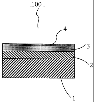
[0014] [Figure 1] This is a schematic view of a section of the transparent
resin
plate.
[Figure 2] This is a spectral atlas of FT-IR showing relations between wave
numbers and the transmittance of the transparent resin plate. F2 laser light
is
irradiated on the unreformed siloxane resin layer and the reformed film region
which are formed on the polycarbonate substrate respectively. Fig. 2A shows
measured effect of the unreformed region, Fig. 2B shows that of the reformed
region,
and Fig. 2C shows that of thermal silicon dioxide.
[Figure 3] This is a microphotography view of the surface of the transparent
resin plate. The Taber Friction Test is carried out to the unreformed siloxane
resin
layer and the reformed hard-coating layer in accordance with JISK7204. Fig. 3A
is
a photograph of the unreformed region and Fig. 3B is that of the reformed
region.
[Figure 41 This is a comparative-photographic view in the film thickness of
the transparent resin plate. Fig. 4A is a microphotography view in the Taber
Friction Test of the surface having the film thickness of 0.3 p. m, Fig.4B is
that
having the film thickness of 0.6 m, and Fig. 4C is that having the film
thickness of
1.0 g m, and Fig. 4D is that having the film thickness of 2.0 p. m.
[Figure 51 This is a view showing a step between the reformed region and
the unreformed region of the transparent resin plate.
[Figure 6] This is a spectral atlas of Examples 3, 4.
[Figure 71 This is a photographic view showing the situation of peeling.
[Figure 8] This is a view showing a characteristic of the transmittance in an
ultraviolet line region of a simple substance of hard-coating film.
EXPLANATION OF REFERENCED NUMERALS
[0015] 1 a substrate
2 a primer layer
3 a hard-coating layer
4 a reformed region
100 a transparent resin plate
4
CA 02715727 2010-08-16
PREFERRED EMBODIMENT OF THE INVENTION
[0016] A film thickness of a silicon dioxide film is preferably made thick to
enhance
the abrasion resistance. In the patent literature 4, the past examples merely
illustrate that reforming into the silicon dioxide can be carried out.
Besides, as to a
thickness, they illustrate a possibility for making a reformed region having
more
than 1 m.
[0017] In advance of the invention, the inventors formed the hard-coating
layer on
the surface of the resin substrate having an area of about 1 cm2, and
confirmed that
the hard-coating layer was reformed into silicon dioxide by vacuum ultraviolet
rays.
[0018] To investigate whether cracks occur on the finished silicon dioxide,
the resin
substrate was dipped into solvent (acetone) which can solve the resin. But,
the
solution of the resin could not be observed at the portion where the silicon
dioxide
film was formed. This indicates that no cracks occur on the silicon dioxide
film
because the solvent penetrated from a crack.
[0019] The inventors further formed the hard-coating film and made an area of
1 cm2
thereof a reformed region having a thickness of 1 ji m or 2 IL m. Then a
friction test
was carried out in accordance with Taber Friction Test. The Taber Friction
Test is a
test wherein a specimen is fitted and rotated on a rotating disk and worn by
loading
on a pair of grindstones. For example, according to Japanese Industrial
Standards
Committee (JISC), JISK7204 is standardized as one of the Taber Friction Test.
As
a result, when the cracks occurred in the hard-coating film of the unreformed
region
during the Friction Test, all of them spread to the reformed region and caused
new
cracks. The load was 500 g, and the number of rotation was 500.
[0020] In reforming the Si¨O¨Si bonds into silicon dioxide (Si02) by an
exposure
light source no greater than 200 nm, oxygen in a reaction atmosphere or oxygen
in
silicon polymer is incorporated into the reformed region. It is considered
that the
volume of the reformed region is changed and an internal stress is kept in the
reformed region itself when oxygen is incorporated into the reformed region.
Further, it is considered that the internal stress is released and the cracks
occurred
on the reformed region when the crack occurs on the hard-coating layer in the
Taber
Friction Test.
[0021] Then, samples in which each film thickness of the reformed region of
silicon
dioxide was under 1 u m were prepared and investigated. As a result, it was
found
out that the cracks did not occur in the Taber Friction Test when the film
thickness
was lower than 0.6 ,u m.
[0022] From the above investigation, in reforming into silicon dioxide, the
film
CA 02715727 2010-08-16
thickness should be made under 0.6 12 m, for example, 0.5 g m. If the reformed
region has the film thickness larger than this, the strength can not be
enhanced.
Adversely, the cracks occur from the inside during use. Accordingly,
controlling the
film thickness of the reformed region becomes an important problem.
[0023] As a light source of vacuum ultraviolet rays having a wavelength
shorter than
200nm, there are an excimer laser, an excimer lamp, and a low pressure mercury
lamp. The usable excimer lasers are Ar2 laser having a wavelength of 126 nm,
F2
laser having a wavelength of 157 nm, ArF excimer laser having a wavelength of
193
nm, KrF excimer laser having a wavelength of 248 nm, and/or XeC1 excimer laser
having a wavelength of 307 nm. In these, the light sources of vacuum
ultraviolet
rays having a wavelength shorter than 200nm are Ar2 laser, F2 laser and ArF
laser.
Besides, the usable excimer lamps are ones each having a wavelength of 126 um
(Ar2), 146 nm (Kr2), and 172 nm (Xe2).
[0024] Theoretically, synthetic quartz glass has a light permeability to a
wavelength
region having vacuum ultraviolet rays of about 145 nm. As to the excimer laser
and
the excimer lamp each having a wavelength shorter than this, absorption for
the
silicon dioxide reformed by the vacuum ultraviolet rays occurs. Accordingly,
in case
of these light sources, because the light does not reach the interior, it is
possible to
reform an extremely thin region of the exposed surface in the hard-coating
layer but
it is difficult to control a thickness of the reformed region.
[0025] Because oxygen absorbs the vacuum ultraviolet rays, a distance from the
light
source of the excimer lamp available for a wavelength region of 172 nm to its
exposed
field is very short, which is less than 3 mm. Therefore, the excimer lamp is
available for a plane transparent plate, but unavailable for a three-
dimensional
transparent plate such as a front glass of a car. An excimer laser easily
controllable
for the light strength is available for the three-dimensional transparent
plate by
controlling in accordance with the distance to the transparent plate.
[0026] Further, even in the light sources of 145 nm ¨ 200 nm, what caused
problems
in an adhesive property of the hard-coating layer for the polycarbonate were
found
out. It was a cause that the vacuum ultraviolet rays permeated the hard-
coating
layer and invaded the primer layer. According to Fig. 8, the silicon polymer
such as
siloxane resin has a good transmissivity in a long-wavelength region about 200
nm,
but the transmissivity radically decreases in a region from about 180 nm to a
short-wavelength. Vacuum ultraviolet rays having a wavelength shorter than 200
urn have an ability to decompose even the polycarbonate substrate used in the
invention. Accordingly, it is considered that the primer layer is decomposed
so as to
6
CA 02715727 2010-08-16
peel easily.
[0027] According to the above-mentioned investigation, when the excimer laser
is
used as a light source, it is preferable to use F2 laser having a wavelength
of 157 nm.
The light of this wavelength does not permeate the siloxane resin.
Accordingly,
when the excimer laser is irradiated to the siloxane resin, the surface
receives high
energy and starts to be reformed into the silicon dioxide. The laser light
permeated
the reformed siloxane resin continues reforming from the surface to the inside
in
order.
[0028] When the excimer lamp is used, it is preferable to use Xe excimer lamp.
The
Xe excimer lamp has a wavelength of 172 nm, which permeates the hard-coating
layer. The permeated light reaches and decomposes the polycarbonate substrate.
Besides, the vacuum ultraviolet rays permeate the hard-coating layer with high
energy, and therefore, it is difficult to control a thickness of the reformed
region. To
solve this problem, an ultraviolet absorbent is added to the hard-coating
layer. In
this case, the ultraviolet absorbent is dispersed in accordance with the film
thickness
of the hard-coating layer so that the light does not permeate the hard-coating
layer.
The hard-coating layer including the ultraviolet absorbent absorbs the light
energy
from the surface side thereof, so that it is reformed. The hard-coating layer
changes
into silicon dioxide by the reformation. Therefore, the transmissivity
increases, so
that the light having high energy can penetrate inwardly further. As a result,
it is
possible to control the film thickness of the reformed region reformed into
the silicon
dioxide from the surface of the hard-coating layer.
[0029] Fig. 1 is a schematic view of a section of the transparent resin plate.
A transparent resin plate 100 comprises a substrate 1, a primer layer 2 and a
hard-coating layer 3. The hard-coating layer 3 is formed on the substrate 1
through
the primer layer 2. The primer layer 2 and the hard-coating layer 3 are
respectively
formed by the dip coating method. On the other hand, a part of the surface of
the
hard-coating layer 3 is formed into a reformed region (a hardened film) 4.
The construction of the transparent resin plate 100 will be explained below.
[0030] The substrate 1 is specifically not limited. However, for the
materials, it is
preferable to use various olefin resins or transparent resins such as acryl
resin,
polycarbonate resin, polyarylate resin, polystyrene resin, polyethylene
terephthalate
resin, styrene polymer and so on.
[0031] The primer layer 2 is provided in order to enhance the shock resistance
or the
adherence between the substrate 1 and the hard-coating layer 3. Besides, in
the
invention, it has an effect to extinguish flaws on the surface of the
substrate 1. The
7
CA 02715727 2010-08-16
primer layer 2 is formed out of various resins such as polyester resin, acryl
resin,
polyurethane resin, epoxy resin, melamine resin, polyolefin resin, urethane
acrylate
resin and so on.
[0032] The hard-coating layer 3 is formed out of silicone polymer, namely,
siloxane
resin. Generally, this siloxane resin is obtained by hydrolyzing siloxane sol,
and this
siloxane sol is obtained by an arcoxysilane-based condensing reaction.
[0033] The reformed region 4 is formed by reforming a part of the surface of
the
hard-coating layer by the laser light irradiation, comprising a thin film
mainly
composed of silicon dioxide.
[0034] Next, a method for producing the transparent resin plate related to the
invention will be explained. The primer layer 2 having a predetermined
thickness is
formed on the resin substrate 1 by the wet method, for example, the dip
coating
method. The substrate 1 is dried at a room temperature for a required time.
Thereafter, it is harden-dried in the atmosphere for a required time by
heating. After
the temperature of the substrate 1 returns to the room temperature, the hard-
coating
layer 3 having the fixed thickness is similarly formed on the primer layer 2
by the wet
method, namely, the dip coating method. After the hard-coating layer 3 is
dried at the
room temperature for a required time, it is harden-dried in the atmosphere for
a
required time by heating. The harden-drying temperature and the necessary time
can be appropriately converted for a kind of materials and the film
thicknesses.
[0035] Then, the surface of the hard-coating layer 3 is exposed to an
irradiation of the
ultraviolet laser light having a wavelength less than 200 nm so as not to
cause an
ablation. Here, the components of the exposed region are reformed to form the
reformed region.
Example
[0036] To further illustrate the transparent resin plate and the method for
producing
the same of the invention, the following examples are given. However, these
examples are intended to illustrate the invention and not to be construed to
limit the
scope of the invention.
(Example 1)
This embodiment is an example wherein the polycarbonate substrate, the
acrylic primer layer and the silicone hard-coating layer were applied as
materials of
the transparent resin plate 100. The transparent resin plate 100 was produced
as
follows. Thereafter, the reformed region 4 of the hard-coating layer 3 was
compared
with the circumferential unreformed region in the property.
[0037] An acryl resin layer 2 having a film thickness of about 4 p. m was
formed on a
8
CA 02715727 2010-08-16
,
polycarbonate substrate 1 by the dip coating method. Then the plate was dried
at the
room temperature, and thereafter, hardened by heating in the atmosphere at a
temperature of 120 C for 70 minutes. After the substrate 1 returned to the
room
temperature, the hard-coating layer 3 having a film thickness of about 4 ji m
was
formed on the acryl resin layer 2 by the dip coating method. The hard-coating
layer 3
was formed out of siloxane resin. Then, the plate was dried at the room
temperature,
and thereafter, harden-dried in the atmosphere at a temperature of 120 C for
60
minutes.
[0038] Next, F2 laser having a wavelength of 157 nm was irradiated on the
surface of
the hard-coating layer 3. An irradiated area was about 10 mm x 25 mm, the
energy
density was about 17 mJ/cm2, pulse frequency was 10 Hz, and irradiation time
was
30 seconds. The reformed region 4 having a thickness of about 0.15 It m was
obtained. Any particular step-like texture can not be observed at the boundary
between the reformed region 4 and the unreformed region.
[0039] Fig. 2 is a spectral atlas of FT-IR (Fourier Transform Infrared
Spectrometer)
showing relations between wave numbers and the transmissivity. Fig. 2A shows a
measurement result of the unreformed region (the hard-coating layer 3), Fig.
2B is the
reformed region 4 (the hardened film), and Fig. 2C is thermal silicon oxide.
In Fig. 2A,
other than stretching vibration (1200 ¨ 1000 cm-1) of Si-0, deformation
vibration
(1270 cm.1) of Si¨CI-13, and C¨H stretching vibration and Si¨C stretching
vibration
of (765 cm-1) which are originated in CH3(2791 cm') are observed. Contrarily,
in Fig.
2B, absorption of 2971 cm-1, 1270 cm-1 or 765 cmq is weak and an absorption
spectrum
like the spectral atlas of Fig. 2C is shown. Accordingly, the reformed region
4 is
considered as having a structure closely related to the characteristic of the
thermal
silicon dioxide mainly composed of silicon dioxide.
[0040] Fig. 3 is a microphotography view of the surface of the hard-coating
layer 3,
showing a test result by the Taber Friction Test in accordance with JISK7204.
Fig. 3A
is a microphotography of the unreformed region and Fig. 3B is a
microphotography of
the reformed region. In the reformed region and the unreformed siloxane resin
layer
surface (the hard-coating layer surface), a big different is observed in flaws
by the
Friction Test. It is confirmed that the hardness of the reformed region
increases.
[0041] Although the above-mentioned example explained a method when the
irradiation area was about 10 mm x 25 mm, the irradiation area can be enlarged
by
irradiating the laser while moving an XY-table on which the substrate 1 is
arranged.
Besides, in the above-mentioned example, the laser reformation required the
irradiation time of 30 seconds at the pulse frequency of 10 Hz per one area.
However,
9
CA 02715727 2010-08-16
the irradiation time can be shortened; for example, it is 3 seconds when the
pulse
frequency is 100 Hz. When the pulse frequency is 1KHz, the irradiation time
can be
shortened in 0.3 seconds.
[0042] Reforming time can be shortened by letting the laser output increase in
the
range where abrasion does not occur.
[00431 The vacuum ultraviolet laser (F2) having a wavelength of 157 nm used in
the
above-mentioned example has an oxygen absorptivity. However, it is possible to
suppress the decrement of the laser light, for example, by filling an optical
path with
nitrogen gas. In this case, vacuuming time is needless because the operation
is not
carried out under vacuum like the CVD.
[0044] In this embodiment, conditions for harden-drying the siloxane resin
layer can
be appropriately changed in order to lighten stress or optimize composition
and
structure of the reformed region. For example, the harden-drying temperature
can be
lowered. Besides, the harden-drying may be carried out under appropriate
conditions
after the reformation not in forming the siloxane resin layer.
[00451 Fig. 4 is a comparison view showing the relation of a thickness of the
reformed
region 4 and a crack, each figure being a microphotography view of a test
result by the
Taber Friction Test. The transparent resin plates each having the reformed
region 4
of the film thickness of 0.6 g m, 1.0 g m or 2.0/2 m were formed the same as
example
1 except the thickness of the reformed region 4 was 0.3 kt m. A thickness of
the acryl
resin layer and a thickness of the silicone polymer layer are both made 4 i.i.
m. The
test result is according to the Taber Friction Test in accordance with
JISK7204. From
the figure, it is confirmed that a crack does not occur when the thickness of
the
reformed region is 0.3 g m and that a crack occurs when a thickness is more
than 0.6
g m. Besides, the more a film thickness is larger, the more the density of the
cracks
increases. It is surmised that the cracks occurs because the reforming region
4 has
compressive stress by expanding the volume because oxygen incorporated by the
laser
reformation forms silicon dioxide. In case the thickness of the reformed
region is
more than 0.6 g m, the cracks occur irrespective of the size of the
transparent glass
substrate. The film thickness is controlled less than 0.6 g m by appropriately
choosing formation conditions of the hard-coating layer 3, the laser light
strength, the
irradiation time, the pulse duration and the frequency so as not to cause the
cracks.
[0046] (Example 2)
The transparent resin plate was formed the same as example 1 except
irradiating the laser on an area where a wiper blade rubbed. The polycarbonate
substrate 1 with the hard-coating layer 3 was arranged on the XY table and
exposed to
CA 02715727 2010-08-16
the irradiation of the laser as moving the XY table. In this case, the motion
of the XY
table was inputted into a controller in advance, and only a reforming area was
deposited as scanning. Since the laser light was equally irradiated on the
deposited
area, there were no step-like texture observed between the reformed region and
the
unreformed region. Accordingly, the abrasion resistance for the wiper blade
was
enhanced (See Fig. 5). Besides, because the internal stress of the reformed
region is
lightened by controlling the film thickness, even if the cracks occur on the
unreformed
region, another crack caused by them can be prevented from transmitting from
the
edge of the reformed region.
[0047] (Example 3)
The reformation was carried out in N2 atmosphere for 180 minutes at Kr2
excimer lamp output energy strength of 3.2 mW/cm2. The thermosetting primer
and
the thermosetting hard-coating layer were formed the same as the above-
mentioned
steps. The reformation into silicon dioxide was confirmed by the surface
analysis
based on the spectral atlas of FT-IR. A vertical line of the spectral atlas of
FT-IR in
the above-mentioned examples shows the transmissivity, whereas it shows a
shielding
rate in this example. Fig. 6A illustrates an observation result before
reforming (after
forming the hard-coating layer), and Fig. 6B illustrates an observation result
after
irradiating the excimer lamp of 146 nm. As shown in Fig. 6B, a forked Si-0
peak is
changed into a single peak and a C¨H peak is decreased or disappeared. In this
case,
the thickness of the reformed region was about 1 a m. In this example,
although the
film thickness was thickened in order to confirm the reformation into silicon
dioxide,
the cracks occurred according to the Taber Friction Test in accordance with
JISK7204.
[0048] In case the film thickness of the reformed region is made under 5 IL m
with
Kr2 excimer lamp, about half irradiation may as well be carried out but it
takes much
time to form the reformed region.
[0049] To reform into the silicon dioxide, according to the gas absorption of
the resin,
oxygen absorbed from the atmosphere is utilized.
[0050] (Example 4)
The reformation was carried out with Xe2 excimer lamp having a wavelength
of 172 nm instead of the Kr2 excimer lamp in Example 3. (For oxygen for
reforming into
silicon dioxide, oxygen absorbed in the resin was utilized.) After forming the
thermosetting primer and the thermosetting hard-coating layer, the resin plate
was
disposed in N2 atmosphere for 15 minutes at a luminous intensity of 35 mW/cm2.
Fig.
6C illustrates the observation result by FT¨IR. According to this result, it
is
confirmed that the reformation into Si02 was carried out the same as the case
of the
11
CA 02715727 2010-08-16
irradiation of 146 nm. The thickness of the reformed region was also about 1
LL m.
Similarly with Example 3, according to the Taber Friction Test in accordance
with
JISK7204, the cracks occurred.
[0051] Besides, an adherence test was carried out to the reformed region in
Example
4 in accordance with JISK5400 (JISC standard, a crosscut tape peeling test).
Peeling
of the hard-coating layer was confirmed. Fig. 7 illustrates the peeling
situation.
(The black lines are flaws of the crosscut.) The tape peeling test is a test
wherein 100
squares of 10 mm X 10 mm are made and pressed with a cellophane tape and
thereafter the number of eyes which stay when the cellophane tape is suddenly
torn off
is counted.
[0052] Although the irradiation time was shortened for around 1 minute and the
film
thickness of the reformed region was thinned in 0.7 g m, the differences were
not
confirmed in the peeling situation by the test in accordance with JISK5400. It
is
inferred that the peeling is not caused by reforming the hard-coating film.
The
hard-coating film of 4 m was formed on a synthetic quartz glass, and then,
the
transmissivity of its simple substance in an ultraviolet ray region was
measured. The
characteristics were shown in Fig. 8, and it was confirmed that the light of
172 nm
permeated around 30 %. However, in this case, the cracks were not confirmed to
occur in the Taber Friction Test in accordance with JISK7204.
[0053] Thus it is considered that the vacuum ultraviolet rays decompose the
bedding
primer resin layer (acryl resin) and deteriorate the adhesion property in a
boundary of
the hard-coating layer and the primer layer.
[0054] Next, an appropriate amount of the ultraviolet absorbent was added to
hard-coating liquid in advance, and filming of the hard-coating layer to
prevent the
reforming ultraviolet rays from permeating was carried out. Then, the
reformation
was carried out under the same condition (in N2 atmosphere for 15 minutes at a
luminous intensity of 35 mW/cm2) instead of the Xe2 excimer lamp. As a result,
peeling of the hard-coating layer was not confirmed in the adherence test in
accordance
with JISK5400. For an ultraviolet absorbent adaptable to the above-mentioned
purpose, metal oxide such as ZnO, TiO, CaO or SnO is used and desirably doped
if
necessary. For example, triazine compounds of an organic ultraviolet absorbent
can
be used. The metal oxides such as ZnO, TiO, CaO and SnO absorb the vacuum
ultraviolet rays to be separated into metal and oxygen, and lose an
ultraviolet
absorbing ability. Accordingly, the vacuum ultraviolet rays arrive from the
surface of
the hard-coating layer to the inside with high energy sequentially, then being
used for
the reformation. In this case, it is considered that some separated oxygen is
12
CA 02715727 2010-08-16
,
incorporated as silicon dioxide.
[0055] The compound of the hard-coating liquid may be changed for one superior
in
shielding property of the wavelength in itself. In this case, a light
absorption end of
the hard-coating liquid is controlled so as to be higher than the wavelength
of the used
light source.
[0056] Although the excimer laser and the excimer lamp were used in the
above-mentioned examples, a low pressure mercury lamp can be also used in the
invention as a light source for irradiating vacuum ultraviolet rays. For
example, the
low pressure mercury lamp of 184.9 nm is usable. When using this lamp, like
the
excimer lamp of 172 nm, the ultraviolet absorbent is added to the hard-coating
layer.
[0057] Although the hard-coating layer 3 was formed on the substrate 1 through
the
primer layer 2 in the above-mentioned examples, it can be directly formed on
the
substrate 1 out of siloxane resin by the dip coating method so as to cover the
substrate
1. In this case also, when utilizing the vacuum ultraviolet rays having a
wavelength
permeating the hard-coating layer 3, it is desirable to dope the hard-coating
layer 3
with the metal oxide such as ZnO, TiO, CaO or SnO. The vacuum ultraviolet rays
decompose the resin components of the substrate 1, thereby making worse the
adhesion property in the boundary of the substrate 1 and the hard-coating
layer 3.
13