Note: Descriptions are shown in the official language in which they were submitted.
CA 02716811 2010-08-25
1
TOUCH PANEL
TECHNICAL FIELD
[0001] The present invention relates to a touch panel which is provided
at the front of a display and is used as an input switch integrated with the
display, and in particular, to a touch panel of the glass-glass type.
BACKGROUND ART
[0002] Fig. 1 shows the configuration of a glass-glass type touch panel
of this kind (resistive film type touch panel) while separating the touch
panel into an upper glass part and a lower glass part. The thickness of an
upper glass substrate 11 is less than that of a lower glass substrate 12.
On the opposing surfaces of the upper and lower glass substrates 11 and
12, transparent conductive film 13 and 14 are formed, respectively.
[0003] Each transparent conductive film 13, 14, serving as a resistive
film, is implemented by an ITO film, for example. At both ends of the
transparent conductive film 13, electrodes 15 and 16 are formed by
application of conductive paste by printing (hereinafter referred to
simply as "printing"). Similarly, electrodes 17 and 18 are formed at both
ends of the transparent conductive film 14 by printing.
[0004] In this example, the electrodes 17 and 18 of the transparent
conductive film 14 are placed at both ends of the transparent conductive
film 14 in regard to the X direction. In contrast, the electrodes 15 and 16
of the transparent conductive film 13 are placed at both ends of the
transparent conductive film 13 in regard to the Y direction. As shown in
Fig. 1, the electrodes 15 and 16 are extended in the X direction to form
CA 02716811 2010-08-25
2
connection parts 15a and 16a, respectively. Each connection part 15a
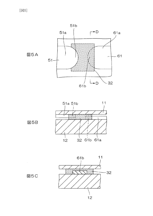
and 16a is narrowed compared to the electrodes 15 and 16 and is formed
in a protruding shape.
[0005] On the surface of the lower glass substrate 12 with the
transparent conductive film 14, extraction patterns 21 - 24 to be used for
applying and detecting voltage are formed by printing. The extraction
patterns 21 and 22 are extracted from the electrodes 17 and 18,
respectively. On the other hand, the extraction patterns 23 and 24 are
formed to have connection parts 23a and 24a at their inner ends,
respectively. The end of each connection part 23a and 24a is formed in a
shape with a U-shaped notch.
[0006] The other ends (outer ends) of the extraction patterns 21 to 24
routed as shown in Fig. 1 are arranged in a line along one side of the
lower glass substrate 12. To the outer ends of the extraction patterns 21
to 24, cables (e.g., FPC cables) for circuit connection (unshown) are
connected. Incidentally, a lot of dot spacers 25 are formed in an array on
the transparent conductive film 14 of the lower glass substrate 12.
[0007] The upper glass substrate 11 and the lower glass substrate 12
configured as above are joined together at their peripheries and
integrated into one body by a seal 26 including spacers. In this state, the
transparent conductive films 13 and 14 face each other.
[0008] The seal 26, which is made of a mixture of thermosetting resin
(e.g., epoxy-based resin) and spacers, is applied and arranged on the
lower glass substrate 12 as shown in Fig. 1. By overlaying the upper
glass substrate 11 on the lower glass substrate 12 and then pressurizing
CA 02716811 2010-08-25
3
and baking the stacked substrates, the upper and lower glass substrates
11 and 12 are joined together while keeping a prescribed gap between
them.
[0009] Incidentally, a cut-out part 26a formed in the frame-shaped seal
26 is used after the upper and lower glass substrates 11 and 12 have been
joined together, as an injecting hole for injecting air into the gap between
the substrates for bulging up the central part of the upper glass substrate
11, that is, for increasing the gap. After the air injection, the cut-out part
26a is sealed up with resin.
[0010] In the above configuration with the upper and lower glass
substrates 11 and 12 joined together, the narrowed connection parts 15a
and 16a of the electrodes 15 and 16 fit in the U-shaped notches of the
connection parts 23a and 24a, respectively, as will be explained later. In
other words, the connection parts 23a and 15a are formed in such shapes
as to couple with each other across a minute gap (ditto for the connection
parts 24a and 16a).
[0011 ] Fig. 2 shows the above situation by focusing on a connecting
part where the connection parts 23a and 15a are connected together. The
connection parts 23a and 15a formed in planer shapes coupling with each
other across a minute gap are connected together via conductive paste 31.
Specifically, the conductive paste 31 is printed on non-end portions (i.e.,
portions other than the ends) of the connection parts 15a and 23a.
[0012] The conductive paste 31 is printed on the non-end portions as
above in order to achieve electrically stable connection between the
connection part 23a and the conductive paste 31 and between the
CA 02716811 2010-08-25
4
connection part 15a and the conductive paste 31, since there is a
possibility that the printing has not been done stably at the ends of the
connection parts 15a and 23a of the electrode 15 and the extraction
pattern 23.
[0013] In the touch panel configured as above, when an arbitrary point
on the panel is depressed, the transparent conductive films 13 and 14
make contact with each other at the depressed point. The X coordinate
of the point can be figured out by applying voltage between both ends of
the transparent conductive film 14 and detecting the voltage through the
transparent conductive film 13. Similarly, the Y coordinate of the point
can be figured out by applying voltage between both ends of the
transparent conductive film 13 and detecting the voltage through the
transparent conductive film 14. The (X, Y) coordinates of the depressed
point can be detected as above.
Patent Literature 1: Japanese Patent Application Laid Open No. 2003-
323260
DISCLOSURE OF THE INVENTION
PROBLEMS TO BE SOLVED BY THE INVENTION
[0014] In the touch panel having the above configuration, the electrodes
and the extraction patterns are formed by printing and baking of
conductive paste such as silver paste. The minimum width necessary for
stable printing of the electrode or extraction pattern (hereinafter referred
to as a "minimum print width") is approximately 0.5 mm at present and it
is widely known that the stable printing can become impossible when the
width of the electrode/pattern is less than the minimum print width. The
CA 02716811 2010-08-25
printing in a width less than the minimum print width can result in
faintness or patchiness of the electrode/pattern.
[00 15] Thus, in order to realize stable printing of the electrodes and the
extraction patterns, the widths dl and d3 (see Fig. 2A) of the edge parts
5 at both edges in regard to the width direction of the connection part 23a
of the extraction pattern 23 and the width d2 of the connection part 15a
of the electrode 15 are all set wider than the minimum print width.
Consequently, the widths of the connection parts 23a and 15a of the
extraction pattern 23 and the electrode 15 are necessitated to be three
times the minimum print width or wider.
[0016] The primary object of the present invention, which has been
made in consideration of the above situation, is to provide a touch panel
in which the widths of the connection parts of the extraction pattern and
the electrode can be reduced compared to conventional touch panels.
MEANS TO SOLVE THE PROBLEMS
[0017] A touch panel according to the present invention comprises:
transparent conductive films formed on opposing surfaces of a
pair of glass substrates to face each other;
an extraction pattern formed on the surface of one glass substrate
with the transparent conductive film and having a connection part;
an electrode provided on the transparent conductive film of the
other glass substrate and having a connection part that is not located in
the same range as the connection part of the extraction pattern in an
extending direction of the connection part of the extraction pattern; and
CA 02716811 2010-08-25
6
a conductive paste connecting the end of the connection part of
the extraction pattern and the end of the connection part of the electrode.
EFFECTS OF THE INVENTION
[0018] By preventing the connection parts of the extraction pattern and
the electrode from being located in the same range in their extending
direction, the widths of the connecting parts of the extraction pattern and
the electrode can be reduced compared to conventional touch panels.
BRIEF DESCRIPTION OF THE DRAWINGS
[0019] Fig. 1 is an exploded perspective view showing the general
configuration of a conventional touch panel;
Fig. 2A is a (transparent) plan view of a connecting part in the
conventional touch panel;
Fig. 2B is a side view of the connecting part;
Fig. 2C is a cross-sectional view of the connecting part taken
along the line D - D shown in Fig. 2A;
Fig. 3 is an exploded perspective view showing the general
configuration of a touch panel in accordance with a first embodiment;
Fig. 4A is a (transparent) plan view of a connecting part in
accordance with the first embodiment;
Fig. 4B is a side view of the connecting part;
Fig. 4C is a cross-sectional view of the connecting part taken
along the line D - D shown in Fig. 4A;
Fig. 5A is a (transparent) plan view of a connecting part in
accordance with a second embodiment;
Fig. 513 is a side view of the connecting part;
CA 02716811 2010-08-25
7
Fig. 5C is a cross-sectional view of the connecting part taken
along the line D - D shown in Fig. 5A;
Fig. 6A is a (transparent) plan view of a connecting part as a
modification;
Fig. 6B is a side view of the connecting part;
Fig. 6C is a cross-sectional view of the connecting part taken
along the line D - D shown in Fig. 6A;
Fig. 7A is a (transparent) plan view of a connecting part as
another modification;
Fig. 7B is a side view of the connecting part;
Fig. 7C is a cross-sectional view of the connecting part taken
along the line D - D shown in Fig. 7A;
Fig. 8A is a (transparent) plan view of a connecting part in
accordance with another embodiment;
Fig. 8B is a side view of the connecting part; and
Fig. 8C is a cross-sectional view of the connecting part taken
along the line D - D shown in Fig. 8A.
BEST MODES FOR CARRYING OUT THE INVENTION
[0020] Referring now to the drawings, a description will be given in
detail of an example of embodiments in accordance with the present
invention. In the following description and figures, components
equivalent to those in Figs. 1 and 2 are assigned the same reference
characters as those in Figs. 1 and 2 and detailed explanation thereof is
omitted for brevity.
[0021] [First Embodiment]
CA 02716811 2010-08-25
8
An example of a first embodiment of the present invention is
shown in Figs. 3 and 4. Electrodes 51 and 52 are provided on the
transparent conductive film 13 of the upper glass substrate 11 similarly
to the electrodes 15 and 16 of the touch panel described in Patent
Literature 1. Meanwhile, extraction patterns 61 and 62 are formed on
the lower glass substrate 12 similarly to the extraction patterns 23 and 24
of the touch panel described in Patent Literature 1.
[0022] In this example, end faces of connection parts 51 a and 52a of the
electrodes 51 and 52 in their extending direction are orthogonal to the
extending direction. Similarly, end faces of connection parts 61a and
62a of the extraction patterns 61 and 62 in their extending direction are
orthogonal to the extending direction. The widths of the electrodes 51
and 52 and the extraction patterns 61 and 62 are set at the minimum print
width, for example. Thus, the widths of the connection parts 51 a and
52a of the electrodes 51 and 52 and the connection parts 61 a and 62a of
the extraction patterns 61 and 62 are also set at the minimum print width,
for example.
[0023] As shown in Fig. 4, the connection parts 51 a and 61 a are
configured so as not to be located in the same range in the extending
direction of the connection parts 51 a and 61 a in the state in which the
upper and lower glass substrates 11 and 12 have been joined together.
Similarly, the connection parts 52a and 62a are configured so as not to
be located in the same range in the extending direction of the connection
parts 52a and 62a in the state in which the upper and lower glass
substrates 11 and 12 have been joined together. Fig. 4A is a plan view of
CA 02716811 2010-08-25
9
a connecting part where the connection parts 51 a and 61 a are connected
together. Fig. 4B is a side view of the connecting part. Fig. 4C is a
cross-sectional view of the connecting part taken along the line D - D
shown in Fig. 4A. Another connecting part where the connection parts
52a and 62a are connected together is also configured similarly.
[0024] Here, "two connection parts are not located in the same range in
the extending direction" means that the two connection parts do not
intrude into each other, that is, two images obtained by projecting the
two connection parts in their width direction do not overlap with each
other. For example, in the touch panel described in Patent Literature 1
(see Fig. 2A), the images obtained by projecting the connection parts 15a
and 23a in the width direction overlap with each other in the range a. In
contrast, in the present invention, the images obtained by projecting the
connection parts 51 a and 61 a in the width direction do not overlap with
each other. Similarly, the images obtained by projecting the connection
parts 52a and 62a in the width direction do not overlap with each other.
[0025] By printing conductive paste 32 (by screen printing, etc.) so that
the conductive paste 32 contacts the ends of the connection parts 51 a and
52a and the ends of the connection parts 61 a and 62a, the electrodes 51
and 52 and the extraction patterns 61 and 62 are electrically connected
together, respectively.
[0026] For electrically stable connection of the connection parts, it has
been considered (as shown in Fig. 2, for example) that not the ends of
the connection parts 15a and 23a but non-end portions (i.e., portions
other than the ends) of the connection parts 15a and 23a have to contact
CA 02716811 2010-08-25
the conductive paste 31 since there is a possibility that the printing has
not been done stably at the ends of the connection parts of the electrode
and the extraction pattern.
[0027] However, it is not absolutely necessary to make the connection
5 part 15a intrude into the U-shaped notch of the connection part 23a and
connect the non-end portions of the connection parts 15a and 23a to the
conductive paste 31 as in the touch panel described in Patent Literature 1.
The present inventor found out that electrical conductivity necessary for
configuring a touch panel can be achieved sufficiently as long as the
10 ends of the connection parts 51 a and 52a and the other connection parts
61 a and 62a, which are not located in the same range in the extending
direction, are in contact with the conductive paste 32.
[0028] By preventing the connection parts 51a and 52a and the other
connection parts 61 a and 62a from being located in the same range in
their extending direction (as in the touch panel of this example), the size
of the connecting part of the electrodes 51 and 52 and the extraction
patterns 61 and 62 can be reduced. Concretely, the widths of the
connection parts 51 a, 52a, 61 a and 62a can be set at the minimum print
width, for example. Further, by the reduction of the widths of the
connection parts, the possibility of occurrence of Newton's rings or
breakage of glass can be reduced compared to the conventional
configuration. Moreover, variation in the operating load can be
eliminated.
[0029] The length L (see Fig. 4) of a contacting part, where the
connection parts 51 a, 52a, 61 a, 62a contact the conductive paste 32, in
CA 02716811 2010-08-25
11
the extending direction is sufficient if L is not less than 12 m twice the
particle diameter (6 m) of the conductor particles (silver particles).
Taking print misalignment and strain misalignment into consideration,
setting the length L at 0.2 mm or longer is sufficient (ditto for other
embodiments described below).
[0030] [Second Embodiment]
Fig. 5 shows an example of the connecting part for the connection
parts 51 a and 61 a in accordance with a second embodiment of the
present invention. The other connecting part for the connection parts
52a and 62a is also configured similarly. In this example, a convex part
51 b in a substantially semicircular shape is formed at the end of the
connection part 51a of the electrode 51. Similarly, a convex part 61b in
a substantially semicircular shape is formed at the end of the connection
part 61 a of the extraction pattern 61.
[0031 ] By printing the conductive paste 32 so that the conductive paste
32 contacts the convex part 51 b of the electrode 51 and the convex part
61 b of the extraction pattern 61, the electrode 51 and the extraction
pattern 61 are electrically connected together via the conductive paste 32.
[0032] If the areas of the parts where the connection parts 51 a, 52a, 61 a
and 62a and the conductive paste 32 overlap with each other (i.e.,
connecting parts) are large, the conductive paste 32 is not squashed
sufficiently when the upper and lower glass substrates 11 and 12 are
joined together and that can lead to a warp of the upper glass substrate
11 and occurrence of Newton's rings. However, by reducing the areas of
the parts where the connection parts 51 a, 52a, 61 a and 62a and the
CA 02716811 2010-08-25
12
conductive paste 32 overlap with each other (i.e., connecting parts) by
letting the convex parts 51 b, 52b, 61 b and 62b at the ends of the
connection parts 51 a, 52a, 61 a and 62a contact the conductive paste 32
as in this example, the warp of the upper glass substrate 11 which can
occur when the upper and lower glass substrates 11 and 12 are joined
together can be reduced. Here, the "part where the connection parts 51 a,
52a, 61 a and 62a and the conductive paste 32 overlap with each other"
means the overlapping parts of the connection parts 51 a, 52a, 61 a and
62a and the conductive paste 32 (i.e., connecting parts) when viewed in
the direction orthogonal to the sheet of Figs. 4A, 5A, 6A or 7A.
[0033] Thus, in the second embodiment, the possibility of occurrence of
Newton's rings or breakage of glass can be reduced, and the variation in
the operating load can be eliminated more efficiently.
[0034] As above, it is unnecessary to make the full width of each of the
connection parts 51 a, 52a, 61 a and 62a contact the conductive paste 32.
[0035] There is a possibility that the printing has not been done stably at
the ends of the connection parts 51 a, 52a, 61 a and 62a of the electrodes
51 and 52 and the extraction patterns 61 and 62. Further, when the
widths of the connection parts 51 a, 52a, 61 a and 62a are set at the
minimum print width, the widths of the convex parts 51 b, 52b, 61 b and
62b are necessitated to be less than the minimum print width and the
convex parts can become faint or patchy due to unstable printing.
However, electrical conductivity necessary for configuring a touch panel
can be achieved sufficiently by making the conductive paste 32 contact
CA 02716811 2010-08-25
13
the convex part 51 b of the electrode 51 and the convex part 61 b of the
extraction pattern 61.
[0036] Incidentally, it is of course possible to set the widths of the
connection parts 51 a, 52a, 61 a and 62a wider than the minimum print
width and also set the widths of the convex parts 51 b, 52b, 61 b and 62b
wider than the minimum print width.
[0037] [Modification]
Effects similar to those of the second embodiment can be
achieved by various types of convex parts 51 b, 52b, 61 b and 62b formed
at the ends of the connection parts 51 a, 52a, 61 a and 62a as long as the
convex parts have a shape protruding in the extending direction of the
connection parts 51 a, 52a, 61 a and 62a.
[0038] For example, it is possible to provide U-shaped notches at the
ends of connection parts 51 a and 61 a and thereby form two convex parts
51 c and 61 c protruding in the extending direction of the connection parts
51 a and 61 a from both edges of the connection parts 51 a and 61 a in
regard to its width direction as shown in Fig. 6. It is also possible to
form a convex part 51 d, 61 d protruding in the extending direction from
the center of each of the connection parts 51 a and 61 a in regard to its
width direction as shown in Fig. 7. The other connection parts 52a and
62a are also formed in similar shapes. By forming the convex part of
connection parts 51 a, 52a, 61 a and 62a in the shape shown in Fig. 6 or
Fig. 7, the size of the parts where the connection parts 51a, 52a, 61a and
62a and the conductive paste 32 overlap with each other can be reduced
further.
CA 02716811 2010-08-25
14
[0039] While there are four parts where the conductive paste 32 contacts
connection parts 51 a, 52a, 61 a and 62a in the touch panels described
above, it is possible to form at least one of the connection parts in the
above shape for the contact with the conductive paste 32. Further, the
shape of the connection parts 51 a and 52a of the electrodes 51 and 52
and that of the connection parts 61 a and 62a of the extraction patterns 61
and 62 may differ from each other.
[0040] Incidentally, the connection between the connection parts 51 a
and 52a of the electrodes 51 and 52 and the connection parts 61 a and 62a
of the extraction patterns 61 and 62 can be achieved more desirably and
stably by retaining the transparent conductive films 13 and 14 and
forming lands from the transparent conductive films 13 and 14 at
positions corresponding to the connection parts 51 a, 52a, 61 a and 62a in
the formation of the transparent conductive films 13 and 14 and
thereafter having the connection parts 51 a, 52a, 61 a and 62a located on
the lands.
[0041] Fig. 8 shows such a state of the touch panel with the lands
formed from the transparent conductive films 13 and 14 by focusing on
the connecting part for the connection parts 51 a and 61 a. In Fig. 8, the
reference numerals "33" and "34" denote the lands.