Note: Descriptions are shown in the official language in which they were submitted.
CA 02716999 2010-08-26
WO 2009/114293 PCT/US2009/035377
METHOD OF FORMING A MAGNETIC TUNNEL JUNCTION DEVICE
I. Field
[0001] The present disclosure is generally related to a method of forming
a magnetic
tunnel junction cell including multiple lateral magnetic domains.
IL Description of Related Art
[0002] In general, widespread adoption of portable computing devices and
wireless
communication devices has increased demand for high-density and low-power non-
volatile memory. As process technologies have improved, it has become possible
to
fabricate magneto-resistive random access memory (MRAM) based on magnetic
tunnel
junction (MTJ) devices. Traditional spin torque tunnel (STT) junction devices
are
typically formed as flat stack structures. Such devices typically have two-
dimensional
magnetic tunnel junction (MTJ) cells with a single magnetic domain. An MTJ
cell
typically includes an anti-ferromagnetic layer (AF), a fixed magnetic layer, a
barrier
layer (i.e., a tunneling oxide layer), and a free magnetic layer, where a bit
value is
represented by a magnetic field induced in the free magnetic layer. A
direction of the
magnetic field of the free layer relative to a direction of a fixed magnetic
field carried
by the fixed magnetic layer determines the bit value.
[0003] Conventionally, to improve data density using MTJ devices, one
technique
includes reducing the size of MTJ devices to put more MTJ devices in a smaller
area.
However, the size of the MTJ devices is limited by the fabrication process
technology.
Another technique involves forming multiple MTJ structures in a single MTJ
device.
For example, in one instance, a first MTJ structure is formed that includes a
first fixed
layer, a first tunnel barrier, and a first free layer. A dielectric material
layer is formed
on the first MTJ structure, and a second MTJ structure is formed on top of the
dielectric
material layer. Such structures increase the density of storage in an X-Y
direction while
increasing a size of the memory array in a z-direction. Unfortunately, such
structures
store only one bit per cell, so the data density in the X-Y direction is
increased at the
expense of area in a Z-direction and cost of manufacture. Further, such
structures
CA 02716999 2010-08-26
WO 2009/114293 PCT/US2009/035377
- 2 -
increase wire-trace routing complexity. Hence, there is a need for improved
memory
devices with greater storage density without increasing a circuit area of each
of the MTJ
cells and that can scale with the process technology.
HI Summary
[0004] In a particular embodiment, a magnetic tunnel junction (MTJ) cell
includes a
substrate having a trench having a first sidewall and a second sidewall. The
MTJ cell
further includes a first lateral electrode disposed within the trench adjacent
to the first
sidewall and a second lateral electrode disposed within the trench adjacent to
the second
sidewall. The MTJ cell further includes a magnetic tunnel junction (MTJ)
structure
disposed within the trench. The MTJ structure includes a fixed magnetic layer
having a
magnetic field with a fixed magnetic orientation, a tunnel junction layer, and
a free
magnetic layer having a magnetic field with a configurable magnetic
orientation. The
MTJ structure may also include an anti-ferromagnetic layer. The MTJ structure
contacts the first lateral electrode at a first lateral interface and contacts
the second
lateral electrode at a second lateral interface. The free magnetic layer that
is adjacent to
the first lateral electrode is adapted to carry a first magnetic domain to
store a first
digital value. The free magnetic layer that is adjacent to the second lateral
electrode is
adapted to carry a second magnetic domain to store a second digital value.
[0005] In another particular embodiment, a method of manufacturing a
magnetic tunnel
junction structure is disclosed that includes forming a trench in a substrate,
depositing a
conductive terminal within the trench, and depositing a magnetic tunnel
junction (MTJ)
structure within the trench. The MTJ structure includes a fixed magnetic layer
having a
fixed magnetic orientation, a tunnel junction layer, and a free magnetic layer
having a
configurable magnetic orientation. The MTJ structure may also include an anti-
ferromagnetic layer. The fixed magnetic layer contacts the conductive terminal
along
an interface that extends substantially normal to a surface of the substrate.
The free
magnetic layer that is adjacent to the conductive terminal carries a magnetic
domain
adapted to store a digital value.
[0006] In still another particular embodiment, a method of forming a
magnetic tunnel
junction structure is disclosed that includes forming a trench in a substrate,
where the
CA 02716999 2010-08-26
WO 2009/114293
PCT/US2009/035377
- 3 -
trench includes a first sidewall, a second sidewall, a third sidewall, a
fourth sidewall,
and a bottom wall. The method includes depositing a first conductive terminal
within
the trench proximate to the first sidewall and depositing a second conductive
terminal
within the trench. The method further includes depositing a magnetic tunnel
junction
(MTJ) structure within the trench. The MTJ structure may include an anti-
ferromagnetic layer, a fixed magnetic layer having a magnetic field with a
fixed
magnetic orientation, a tunnel junction layer, and a free magnetic layer
having a
magnetic field with a configurable magnetic orientation. The fixed magnetic
layer
contacts the first, the second, the third, and the fourth sidewalls at
respective first,
second, third, and fourth lateral interfaces and contacts the bottom wall at a
bottom
interface. The free magnetic layer that is adjacent to the first conductive
terminal is
adapted to carry a first magnetic domain to store a first digital value and
the free
magnetic layer that is adjacent to the second conductive terminal is adapted
to carry a
second magnetic domain to store a second digital value.
[0007] One particular advantage provided by embodiments of the magnetic
tunnel
junction (MTJ) device is provided in that multiple data bits may be stored at
a single
MTJ cell. In this instance, a data storage density of a single bit MTJ cell
may be
doubled, tripled or quadrupled, depending on the particular implementation.
[0008] Another particular advantage is provided in that lateral electrodes
provide a
shorter contact distance, enhancing efficiency and reducing parasitic
resistances and
capacitances due to wiring.
[0009] Still another advantage is that the multiple bit MTJ cell can scale
with process
technology, allowing for multi-bit MTJ cells even as the MTJ cell size
decreases.
[0010] Still another particular advantage is provided in that the MTJ cell
can include
multiple independent magnetic domains to store multiple data bits. In a
particular
embodiment, the MTJ cell can include multiple sidewalls (extending vertically
from a
planar surface of a substrate), where each of the multiple sidewalls carries a
unique
lateral magnetic domain to store a data bit. Additionally, the MTJ cell can
include a
bottom wall including a horizontal magnetic domain to store another data bit.
CA 02716999 2013-02-25
74769-3065
-4-
100111 Yet another particular advantage is provided in that the MTJ
cell can include
multiple independent magnetic domains. Each of the multiple independent
magnetic domains
may be written to or read from without changing data stored at other magnetic
domains within
the MTJ cell.
[0011a] According to one aspect, there is provided a method of
manufacturing a
magnetic tunnel junction device, the method comprising: forming a trench in a
substrate;
depositing a conductive terminal within the trench, wherein depositing the
conductive
terminal comprises forming a first conductive terminal within the trench to
form a first lateral
electrode and forming a second conductive terminal within the trench to form a
second lateral
electrode; and depositing a magnetic tunnel junction (MTJ) structure within
the trench, the
MTJ structure including a fixed magnetic layer having a fixed magnetic
orientation, a tunnel
junction layer, and a free magnetic layer having a configurable magnetic
orientation, the fixed
magnetic layer coupled to the conductive terminal along an interface that
extends substantially
normal to a surface of the substrate, the free magnetic layer adjacent to the
conductive
terminal to carry a magnetic domain adapted to store a digital value.
[0011b] According to another aspect, there is provided a method of
forming a magnetic
tunnel junction device, the method comprising: forming a trench in a
substrate, the trench
including a first sidewall, a second sidewall, a third sidewall, a fourth
sidewall, and a bottom
wall; depositing a first conductive terminal within the trench proximate to
the first sidewall
and depositing a second conductive terminal within the trench; depositing a
magnetic tunnel
junction (MTJ) structure within the trench, the MTJ structure including a
fixed magnetic layer
having a magnetic field with a fixed magnetic orientation, a tunnel junction
layer, and a free
magnetic layer having a magnetic field with a configurable magnetic
orientation, the MTJ
structure adjacent to the first, the second, the third, and the fourth
sidewalls at respective first,
second, third, and fourth lateral interfaces and adjacent to the bottom wall
at a bottom
interface, wherein the free magnetic layer includes a first portion adjacent
to the first
conductive terminal adapted to carry a first magnetic domain to store a first
digital value and
the free magnetic layer includes a second portion adjacent to the second
conductive terminal
adapted to carry a second magnetic domain to store a second digital value; and
selectively
CA 02716999 2013-02-25
74769-3065
- 4a -
removing a portion of the MTJ structure that is adjacent to the fourth
sidewall to create an
opening such that the MTJ structure is substantially u-shaped.
[0011c] According to still another aspect, there is provided a
magnetic tunnel junction
(MTJ) device comprising: a substrate including a trench having a first
sidewall and a second
sidewall; a first lateral electrode disposed within the trench adjacent to the
first sidewall; a
second lateral electrode disposed within the trench adjacent to the second
sidewall; a magnetic
tunnel junction (MTJ) structure disposed within the trench, the MTJ structure
including a
fixed magnetic layer having a magnetic field with a fixed magnetic
orientation, a tunnel
junction layer, and a free magnetic layer having a magnetic field with a
configurable magnetic
orientation, the MTJ structure contacting the first lateral electrode at a
first lateral interface
and contacting the second lateral electrode at a second lateral interface; and
a bottom
electrode within the trench adjacent to a bottom wall; wherein the free
magnetic layer includes
a first portion adjacent to the first lateral electrode adapted to carry a
first magnetic domain to
store a first digital value; wherein the free magnetic layer includes a second
portion adjacent
to the second lateral electrode adapted to carry a second magnetic domain to
store a second
digital value; and wherein the free magnetic layer includes a bottom portion
adjacent to the
bottom electrode adapted to carry a bottom magnetic domain to store a bottom
digital value.
[0011d] According to yet another aspect, there is provided a magnetic
tunnel junction
(MTJ) device comprising: a substrate including a trench; a conductive terminal
disposed
within the trench, wherein the conductive terminal comprises: a first
conductive terminal
disposed within the trench, wherein the first conductive terminal forms a
first electrode; and a
second conductive terminal disposed within the trench, wherein the second
conductive
terminal forms a second electrode; and a magnetic tunnel junction (MTJ)
structure disposed
within the trench, the MTJ structure including a fixed magnetic layer having a
fixed magnetic
orientation, a tunnel junction layer, and a free magnetic layer having a
configurable magnetic
orientation, the fixed magnetic layer coupled to the conductive terminal along
an interface that
extends substantially normal to a surface of the substrate, the free magnetic
layer proximate to
the conductive terminal to carry a magnetic domain configured to represent a
digital value,
wherein the fixed magnetic layer includes a first portion coupled to the first
conductive
terminal via the anti-ferromagnetic layer along a first interface that extends
substantially
CA 02716999 2013-02-25
74769-3065
- 4b -
normal to a surface of the substrate, wherein the fixed magnetic layer
includes a second
portion coupled to the second conductive terminal via the anti-ferromagnetic
layer along a
second interface that extends substantially normal to the surface of the
substrate, and wherein
the fixed magnetic layer includes a bottom portion that extends substantially
parallel to the
surface of the substrate.
[0011e] According to a further aspect, there is provided a method of
forming a
magnetic tunnel junction device, the method comprising: forming a trench in a
substrate, the
trench including a plurality of sidewalls and a bottom wall; depositing a
first conductive
material within the trench proximate to one of the plurality of sidewalls and
depositing a
second conductive material within the trench; depositing a magnetic tunnel
junction (MTJ)
structure within the trench, the MTJ structure including a fixed magnetic
layer having a
magnetic field with a fixed magnetic orientation, a tunnel junction layer, and
a free magnetic
layer having a magnetic field with a configurable magnetic orientation; and
selectively
removing a portion of the MTJ structure to create an opening such that the MTJ
structure is
substantially u-shaped.
1001111 According to yet a further aspect, there is provided a
magnetic tunnel junction
(MTJ) device comprising: a substrate including a trench having a first
sidewall and a second
sidewall; a first electrode disposed within the trench adjacent to the first
sidewall; a second
electrode disposed within the trench adjacent to the second sidewall; a
magnetic tunnel
junction (MTJ) structure disposed within the trench, the MTJ structure
including a fixed
magnetic layer having a magnetic field with a fixed magnetic orientation, a
tunnel junction
layer, and a free magnetic layer having a magnetic field with a configurable
magnetic
orientation, the MTJ structure contacting the first electrode at a first
interface and contacting
the second electrode at a second interface; and a bottom electrode disposed
within the trench
adjacent to a bottom wall of the trench; wherein the free magnetic layer
includes a bottom
portion adjacent to the bottom electrode, the bottom portion configured to
carry a magnetic
domain to store a digital value.
CA 02716999 2013-02-25
74769-3065
- 4c -
[0012] Other aspects, advantages, and features of the present
disclosure will become
apparent after review of the entire application, including the following
sections: Brief
Description of the Drawings, Detailed Description, and the Claims.
IV. Brief Description of the Drawings
[0013] FIG. 1 is a cross-sectional diagram of a particular illustrative
embodiment of a
magnetic tunnel junction (MTJ) stack including lateral magnetic domains;
[0014] FIG. 2 is top view of a particular illustrative embodiment of
a circuit device
including an MTJ cell having multiple lateral magnetic domains;
[0015] FIG. 3 is a cross-sectional diagram of the circuit device of
FIG. 2 taken along
line 3-3 in FIG. 2;
[0016] FIG. 4 is a cross-sectional diagram of the circuit device of
FIG. 2 taken along
line 4-4 in FIG. 2;
[0017] FIG. 5 is top view of a second particular illustrative
embodiment of a circuit
device including an MTJ cell having multiple lateral magnetic domains;
[0018] FIG. 6 is a cross-sectional diagram of the circuit device of FIG. 5
taken along
line 6-6 in FIG. 5;
[0019] FIG. 7 is a cross-sectional diagram of the circuit device of
FIG. 5 taken along
line 7-7 in FIG. 5;
[0020] FIG. 8 is top view of a third particular illustrative
embodiment of a circuit
device including an MTJ cell having multiple lateral magnetic domains;
[0021] FIG. 9 is a cross-sectional diagram of the circuit device of
FIG. 8 taken along
line 9-9 in FIG. 8;
CA 02716999 2010-08-26
WO 2009/114293
PCT/US2009/035377
- 5 -
[0022] FIG. 10 is a cross-sectional diagram of the circuit device of FIG.
8 taken along
line 10-10 in FIG. 8;
[0023] FIG. 11 is top view of a fourth particular illustrative embodiment
of a circuit
device including an MTJ cell having multiple lateral magnetic domains;
[0024] FIG. 12 is a cross-sectional diagram of the circuit device of FIG.
11 taken along
line 12-12 in FIG. 11;
[0025] FIG. 13 is a cross-sectional diagram of the circuit device of FIG.
11 taken along
line 13-13 in FIG. 11;
[0026] FIG. 14 is top view of a fifth particular illustrative embodiment
of a circuit
device including an MTJ cell having multiple lateral magnetic domains;
[0027] FIG. 15 is a cross-sectional diagram of the circuit device of FIG.
14 taken along
line 15-15 in FIG. 14;
[0028] FIG. 16 is a cross-sectional diagram of the circuit device of FIG.
14 taken along
line 16-16 in FIG. 14;
[0029] FIG. 17 is top view of a sixth particular illustrative embodiment
of a circuit
device including an MTJ cell having multiple lateral magnetic domains;
[0030] FIG. 18 is a cross-sectional diagram of the circuit device of FIG.
17 taken along
line 18-18 in FIG. 17;
[0031] FIG. 19 is a cross-sectional diagram of the circuit device of FIG.
17 taken along
line 19-19 in FIG. 17;
[0032] FIG. 20 is top view of a seventh particular illustrative embodiment
of a circuit
device including an MTJ cell having multiple lateral magnetic domains;
[0033] FIG. 21 is a cross-sectional diagram of the circuit device of FIG.
20 taken along
line 21-21 in FIG. 20;
CA 02716999 2010-08-26
WO 2009/114293 PCT/US2009/035377
- 6 -
[0034] FIG. 22 is a cross-sectional diagram of the circuit device of FIG.
20 taken along
line 22-22 in FIG. 20;
[0035] FIG. 23 is top view of a eighth particular illustrative embodiment
of a circuit
device including an MTJ cell having multiple lateral magnetic domains;
[0036] FIG. 24 is a cross-sectional diagram of the circuit device of FIG.
23 taken along
line 24-24 in FIG. 23;
[0037] FIG. 25 is a cross-sectional diagram of the circuit device of FIG.
23 taken along
line 25-25 in FIG. 23;
[0038] FIG. 26 is a top view of a free layer of an MTJ cell having
multiple lateral
magnetic domains configured in a zero-value state;
[0039] FIG. 27 is a cross-sectional view of an MTJ cell including the free
layer of FIG.
26 illustrating a write current to configure the magnetic domains of the free
layer to
represent a zero value;
[0040] FIG. 28 is cross-sectional view of the free layer of FIG. 26 taken
along line 28-
28 in FIG. 26;
[0041] FIG. 29 is a cross-sectional view of the free layer of FIG. 26
taken along line 29-
29 in FIG. 26;
[0042] FIG. 30 is a top view of a free layer of an MTJ cell having
multiple lateral
magnetic domains configured in a one-value state;
[0043] FIG. 31 is a cross-sectional view of an MTJ cell including the free
layer of FIG.
30 illustrating a write current to configure the magnetic domains of the free
layer to
represent a one value;
[0044] FIG. 32 is cross-sectional view of the free layer of FIG. 30 taken
along line 32-
32 in FIG. 30;
[0045] FIG. 33 is a cross-sectional view of the free layer of FIG. 30
taken along line 33-
33 in FIG. 30;
CA 02716999 2010-08-26
WO 2009/114293 PCT/US2009/035377
- 7 -
[0046] FIG. 34 is a cross-sectional view of a particular embodiment of a
MTJ cell;
[0047] FIG. 35 is a cross-sectional view of another particular embodiment
of an MTJ
cell that provides an increased resistance;
[0048] FIG. 36 is a cross-sectional view of an MTJ cell having a single
switch device to
access a single stored value;
[0049] FIG. 37 is a cross-sectional diagram of an MTJ cell having two
switch devices to
access two stored values;
[0050] FIG. 38 is a cross-sectional diagram of an MTJ cell having three
switch devices
to access three stored values;
[0051] FIGs. 39-40 are flow diagrams of a particular illustrative
embodiment of a
method of forming a magnetic tunnel junction (MTJ) structure having multiple
lateral
magnetic domains;
[0052] FIG. 41 is a flow diagram of a second particular illustrative
embodiment of a
method of forming a magnetic tunnel junction (MTJ) structure having multiple
lateral
magnetic domains;
[0053] FIG. 42 is a flow diagram of a third particular illustrative
embodiment of a
method of forming a magnetic tunnel junction (MTJ) structure having multiple
lateral
magnetic domains; and
[0054] FIG. 43 is a block diagram of a wireless communication device
including
memory circuits comprises of MTJ cells.
V. Detailed Description
[0055] FIG. 1 is a cross-sectional diagram of a particular illustrative
embodiment of a
magnetic tunnel junction (MTJ) cell 100 including lateral magnetic domains.
The MTJ
cell 100 includes a magnetic tunnel junction (MTJ) structure 104 having an MTJ
stack
106, a center electrode 108, a first lateral electrode 110, and a second
lateral electrode
112. The MTJ stack 106 includes a fixed magnetic layer 114 that carries a
magnetic
domain having a fixed magnetic orientation, a tunnel barrier layer 116, and a
free
CA 02716999 2010-08-26
WO 2009/114293 PCT/US2009/035377
- 8 -
magnetic layer 118 having a configurable magnetic orientation. The MTJ stack
106 may
also include an anti-ferromagnetic (AF) layer (not shown) that pins the fixed
magnetic
layer 114. The MTJ stack 106 may also include additional layers (not shown).
The
fixed magnetic layer 114 is coupled to the first lateral electrode 110 via the
AF layer at
first lateral interface 120 and contacts the second lateral electrode 112 at a
second lateral
interface 122. It should be understood that the fixed magnetic layer 114 and
the free
magnetic layer 118 may be switched, such that the free magnetic layer 118
contacts the
first and second lateral electrodes 110 and 112 at the first and second
lateral interfaces
120 and 122, respectively. In general, the free magnetic layer 118 has a first
portion
that carries a first magnetic domain 124 (illustrated at 2612 in FIG. 26)
adjacent to the
first lateral electrode 110 and has a second portion that carries a second
magnetic
domain 126 (illustrated at 2616 in FIG. 26) adjacent to the second lateral
electrode 112.
[0056] In a particular embodiment, the dimensions of the MTJ cell 100
(i.e., length,
width, and depth) determine an orientation of a magnetic domain within the
free layer
118. In particular, the magnetic domain along a particular wall aligns in a
direction
corresponding to a longest dimension of the particular wall. If the wall has a
depth that
is greater than its length, the magnetic domain is oriented in a direction of
the depth. In
contrast, if the wall has a length that is greater than the depth, the
magnetic domain is
oriented in a direction of the length. The particular direction of the
magnetic field
associated with the magnetic domain of the free layer 118 relative to a fixed
direction of
a magnetic field associated with the magnetic domain of the fixed layer 114
represents a
data bit value.
[0057] In another particular embodiment, the fixed magnetic layer 114 and
the free
magnetic layer 118 are formed from a ferromagnetic material. The tunnel
barrier layer
116 may be formed from oxidation of metal material, such as magnesium oxide
(MgO).
A read current may be applied via the center electrode 108 and the lateral
electrodes 110
and 112 to read data bit values represented by the first magnetic domain 124
and the
second magnetic domain 126. In a particular example, the first magnetic domain
124
and the second magnetic domain 126 may be adapted to represent unique data bit
values.
CA 02716999 2010-08-26
WO 2009/114293 PCT/US2009/035377
- 9 -
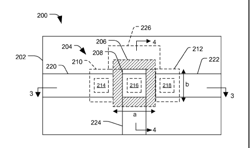
[0058] FIG. 2 is top view of a particular illustrative embodiment of a
circuit device 200
including an MTJ cell having multiple lateral magnetic domains. The circuit
device 200
includes a substrate 202. The substrate 202 includes a magnetic tunnel
junction (MTJ)
structure 204 that has an MTJ stack 206, a center electrode 208, a first
lateral electrode
210, and a second lateral electrode 212. The MTJ stack 206 has a length (a)
and a width
(b), where the length (a) is greater than the width (b). The substrate 202
includes a first
via 214 coupled to the first lateral electrode 210, a center via 216 coupled
to the center
electrode 208, and a second via 218 coupled to the second lateral electrode
212. The
substrate 202 also includes a first wire trace 220 coupled to the first via
214, a second
wire trace 222 coupled to the second via 218, and a third wire trace 224
coupled to the
center via 216. The substrate 202 also includes a process opening 226. In a
particular
embodiment, the MTJ structure 204 is adapted to store a first data value, such
as a first
bit value, and a second data value, such as a second bit value, within a free
layer of the
MTJ stack 206 that is adjacent to the first and second lateral electrodes 210
and 212.
[0059] FIG. 3 is a cross-sectional diagram 300 of the circuit device 200
of FIG. 2 taken
along line 3-3 in FIG. 2. The diagram 300 illustrates the substrate 202
including a first
inter-layer dielectric layer 332, a first cap layer 334, a second inter-layer
dielectric layer
336, a second cap layer 338, a third cap layer 340, a third inter-layer
dielectric layer
342, and a fourth inter-layer dielectric layer 344. The substrate 202 includes
a first
surface 360 and a second surface 370. The substrate 202 also includes the MTJ
structure 204 including the MTJ stack 206. The first lateral electrode 210,
the second
lateral electrode 212, and the MTJ stack 206 are disposed within a trench in
the
substrate 202. The trench has a depth (d). The substrate 202 includes the
first, second
and third wire traces 220, 222, and 224 deposited and patterned at the first
surface 360.
The first wire trace 220 is coupled to the first via 214, which extends from
the first wire
trace 220 to the first lateral electrode 210. The second wire trace 222 is
coupled to the
second via 218, which extends from the second wire trace 222 to the second
lateral
electrode 212. The third wire trace 224 is coupled to the center via 216,
which extends
from the third wire trace 224 to the center (top) electrode 208. The center
electrode 208
is coupled to the MTJ stack 206.
CA 02716999 2010-08-26
WO 2009/114293 PCT/US2009/035377
- 10 -
[0060] In general, the MTJ stack 206 is adapted to store a first data bit
value within a
first portion of the free layer of the MTJ stack 206 that is adjacent to the
first lateral
electrode 210. The MTJ stack 206 is also adapted to store a second data bit
value within
a second portion of the free layer of the MTJ stack 206 that is adjacent to
the second
lateral electrode 212. A data bit value can be read from the MTJ stack 206 by
applying
a voltage between the third wire trace 224 and the first wire trace 220 or the
second wire
trace 222 and by comparing a current at the first wire trace 220 and/or the
second wire
trace 222 to a reference current. Alternatively, a data bit value may be
written to the
MTJ stack 206 by applying a write current between the first wire trace 220 and
the third
wire trace 224 or between the second wire trace 222 and the third wire trace
224. In a
particular embodiment, the width (b) of the MTJ stack 206 illustrated in FIG.
2 is
greater than the depth (d), and respective magnetic domains carried by a free
layer
within the MTJ stack 206 adjacent to the lateral electrodes 210 and 212 extend
in a
direction that is substantially parallel to the surface 360 of the substrate
202 in a
direction of the width (b) of the MTJ stack 206 (i.e., into or out from the
page view of
FIG. 3). If the width (b) of the MTJ stack 206 is less than the depth (d),
respective
magnetic fields of the free layer within the MTJ stack 206 adjacent to the
lateral
electrodes 210 and 212 may be vertical, i.e. along the trench depth direction.
Generally,
the MTJ structures illustrated in FIGs. 2-13 may be patterned by reverse
trench photo-
etch processes and MTJ Chemical-Mechanical Polishing (CMP) processes to
control
trench dimensions, and therefore to control the MTJ dimensions.
[0061] FIG. 4 is a cross-sectional diagram 400 of the circuit device 200
of FIG. 2 taken
along line 4-4 in FIG. 2. The diagram 400 includes the substrate 202 having
the first
inter-layer dielectric layer 332, the first cap layer 334, the second inter-
layer dielectric
layer 336, the second cap layer 338, the third cap layer 340, the third inter-
layer
dielectric layer 342, and the fourth inter-layer dielectric layer 344. The
substrate 202
includes the MTJ stack 206, the top electrode 208, and a center via 216 that
extends
from the third wire trace 224 to the top electrode 208. The substrate 202 also
includes
the process opening 226, which may be formed by selectively removing a portion
of the
MTJ structure 204 and filled by depositing an inter-layer dielectric material
within the
processing opening 226.
CA 02716999 2010-08-26
WO 2009/114293 PC T/US2009/035377
- 11 -
[0062] In a particular illustrative embodiment, the MTJ structure 204 is a
substantially
u-shaped structure including three sidewalls and a bottom wall. The MTJ
structure 204
can include lateral electrodes, such as the first and second lateral
electrodes 210 and
212, that are associated with respective sidewalls and can include a bottom
electrode
that is associated with the bottom wall. Additionally, the MTJ structure 204
is adapted
to store up to four unique data bits.
[0063] FIG. 5 is top view of a particular illustrative embodiment of a
circuit device 500
including an MTJ cell having multiple lateral magnetic domains. The circuit
device 500
includes a substrate 502. The substrate 502 includes a magnetic tunnel
junction (MTJ)
structure 504 that has an MTJ stack 506, a center electrode 508, a first
lateral electrode
510, and a second lateral electrode 512. The MTJ stack 506 has a length (a)
and a width
(b). The substrate 502 includes a first via 514 coupled to the first lateral
electrode 510,
a center via 516 coupled to the center electrode 508, and a second via 518
coupled to the
second lateral electrode 512. The substrate 502 also includes a first wire
trace 520
coupled to the first via 514, a second wire trace 522 coupled to the second
via 518, and
a third wire trace 524 coupled to the center via 516. The substrate 502 also
includes a
process opening 526. In a particular embodiment, the MTJ structure 504 is
adapted to
store a first data bit value and a second data bit value within a free layer
of the MTJ
stack 506 that is adjacent to the first and second lateral electrodes 510 and
512.
[0064] FIG. 6 is a cross-sectional diagram 600 of the circuit device 500
of FIG. 5 taken
along line 6-6 in FIG. 5. The diagram 600 illustrates the substrate 502
including a first
inter-layer dielectric layer 630, a second inter-layer dielectric layer 632, a
first cap layer
634, a third inter-layer dielectric layer 636, a second cap layer 638, a third
cap layer
640, a fourth inter-layer dielectric layer 642, and a fifth inter-layer
dielectric layer 644.
The substrate 502 includes a first surface 660 and a second surface 670. The
substrate
502 also includes the MTJ structure 504 including the MTJ stack 506. The first
lateral
electrode 510, the second lateral electrode 512, and the MTJ stack 506 are
disposed
within a trench in the substrate 502. The trench has a depth (d). The
substrate 502
includes the third wire trace 524 deposited and patterned at the first surface
660 and
includes the first and second wire traces 520 and 522 deposited and patterned
at the
second surface 670. The first wire trace 520 is coupled to the first via 514,
which
CA 02716999 2010-08-26
WO 2009/114293 PCT/US2009/035377
- 12 -
extends from the first wire trace 520 to the first lateral electrode 510. The
second wire
trace 522 is coupled to the second via 518, which extends from the second wire
trace
522 to the second lateral electrode 512. The third wire trace 524 is coupled
to the center
via 516, which extends from the third wire trace 524 to the center (top)
electrode 508.
The center electrode 508 is coupled to the MTJ stack 506.
[0065] In general, the MTJ stack 506 is adapted to store a first data bit
value within a
free layer of the MTJ stack 506 that is adjacent to the first lateral
electrode 510. The
MTJ stack 506 is also adapted to store a second data bit value within the free
layer of
the MTJ stack 506 that is adjacent to the second lateral electrode 512. A data
bit value
can be read from the MTJ stack 506 by applying a voltage between the third
wire trace
524 and the first wire trace 520 or the second wire trace 522 and by comparing
a current
at the first wire trace 520 and/or the second wire trace 522 to a reference
current.
Alternatively, a data bit value may be written to the MTJ stack 506 by
applying a write
current between the first wire trace 520 and the third wire trace 524 or
between the
second wire trace 522 and the third wire trace 524. In a particular
embodiment, the
width (b) of the MTJ stack 506 illustrated in FIG. 5 is greater than the depth
(d), and
respective magnetic domains carried by a free layer within the MTJ stack 506
adjacent
to the lateral electrodes 510 and 512 extend in a direction that is
substantially parallel to
the surface 660 of the substrate 502 in a direction of the width (b) of the
MTJ stack 506
(i.e., into or out from the page view of FIG. 6). If width (b) of the MTJ
stack 506 is
smaller than the depth (d), respective magnetic fields of free layer within
the MTJ stack
506 adjacent to the lateral electrode 510 and 512 may be vertical along the
trench depth
direction.
[0066] FIG. 7 is a cross-sectional diagram 700 of the circuit device 500
of FIG. 5 taken
along line 7-7 in FIG. 5. The diagram 700 includes the substrate 502 having
the second
inter-layer dielectric layer 632, the first cap layer 634, the third inter-
layer dielectric
layer 636, the second cap layer 638, the third cap layer 640, the fourth inter-
layer
dielectric layer 642, and the fifth inter-layer dielectric layer 644. The
substrate 502
includes the MTJ stack 506, the top electrode 508, and a center via 516 that
extends
from the third wire trace 524 to the top electrode 508. The substrate 502 also
includes
the process opening 526, which may be formed by selectively removing a portion
of the
CA 02716999 2010-08-26
WO 2009/114293 PCT/US2009/035377
- 13 -
MTJ structure 504 and filled by depositing an inter-layer dielectric material
within the
processing opening 526.
[0067] In a particular illustrative embodiment, the MTJ structure 504 is a
substantially
u-shaped structure including three sidewalls and a bottom wall. The MTJ
structure 504
can include lateral electrodes, such as the first and second lateral
electrodes 510 and
512, that are associated with respective sidewalls and can include a bottom
electrode
that is associated with the bottom wall. Additionally, the MTJ structure 504
is adapted
to store up to four unique data bits.
[0068] FIG. 8 is top view of a third particular illustrative embodiment of
a circuit
device 800 including an MTJ cell having multiple lateral magnetic domains. The
circuit
device 800 includes a substrate 802. The substrate 802 includes a magnetic
tunnel
junction (MTJ) structure 804 that has an MTJ stack 806, a center electrode
808, a first
lateral electrode 810, a second lateral electrode 812, and a third lateral
electrode 1050.
The MTJ stack 806 has a length (a) and a width (b), where the length (a) is
greater than
the width (b). The substrate 802 includes a first via 814 coupled to the first
lateral
electrode 810, a center via 816 coupled to the center electrode 808, a second
via 818
coupled to the second lateral electrode 812, and a third via 827 coupled to
the third
lateral electrode 1050. The substrate 802 also includes a first wire trace 820
coupled to
the first via 814, a second wire trace 822 coupled to the second via 818, and
a third wire
trace 824 coupled to the center via 816. The substrate 802 also includes a
process
opening 826. The substrate 802 also includes a fourth wire trace 828 coupled
to a third
via 827. In a particular embodiment, the MTJ structure 804 is adapted to store
a first
data bit value within a first portion free layer of the MTJ stack 806 that is
adjacent to the
first lateral electrode 810, a second data bit value within a second portion
of the free
layer that is adjacent to the second lateral electrode 812, and a third data
bit value within
a third portion of the free layer that is adjacent to the third lateral
electrode 1050.
[0069] FIG. 9 is a cross-sectional diagram 900 of the circuit device 800
of FIG. 8 taken
along line 9-9 in FIG. 8. The diagram 900 illustrates the substrate 802
including a first
inter-layer dielectric layer 930, a second inter-layer dielectric layer 932, a
first cap layer
934, a third inter-layer dielectric layer 936, a second cap layer 938, a third
cap layer
940, a fourth inter-layer dielectric layer 942, and a fifth inter-layer
dielectric layer 944.
CA 02716999 2010-08-26
WO 2009/114293
PCT/US2009/035377
- 14 -
The substrate 802 includes a first surface 960 and a second surface 970. The
substrate
802 also includes the MTJ structure 804 including the MTJ stack 806. The first
lateral
electrode 810, the second lateral electrode 812, and the MTJ stack 806 are
disposed
within a trench in the substrate 802. The trench has a depth (d). The
substrate 802
includes the third wire trace 824 deposited and patterned at the first surface
960 and
includes the first and second wire traces 820 and 822 deposited and patterned
at the
second surface 970. The first wire trace 820 is coupled to the first via 814,
which
extends from the first wire trace 820 to the first lateral electrode 810. The
second wire
trace 822 is coupled to the second via 818, which extends from the second wire
trace
822 to the second lateral electrode 812. The third wire trace 824 is coupled
to the center
via 816, which extends from the third wire trace 824 to the center (top)
electrode 808.
The center electrode 808 is coupled to the MTJ stack 806.
[0070] In
general, the MTJ stack 806 is adapted to store a first data bit value within a
first portion of the free layer of the MTJ stack 806 that is adjacent to the
first lateral
electrode 810. The MTJ stack 806 is also adapted to store a second data bit
value within
a second portion of the free layer of the MTJ stack 806 that is adjacent to
the second
lateral electrode 812. The MTJ stack 806 is also adapted to store a third data
bit value
within a third portion of the free layer of the MTJ stack 806 that is adjacent
to the third
lateral electrode 1050. A data value can be read from the MTJ stack 806 by
applying a
voltage between the third wire trace 824 and the first wire trace 820, the
second wire
trace 822, or the fourth wire trace 828 and by comparing a current at the
third wire trace
824 or at the first wire trace 820, the second wire trace 822, or the fourth
wire trace 828
to a reference current. Alternatively, a data value may be written to the MTJ
stack 806
by applying a write current between the first wire trace 820, or the second
wire trace
822, or the fourth wire trace 828, and the third wire trace 824. In a
particular
embodiment, the length (a) and the width (b) of the MTJ stack 806 illustrated
in FIG. 8
are greater than the depth (d), and respective magnetic domains carried by a
free layer
within the MTJ stack 806 adjacent to the lateral electrodes 810, 812, and 1050
extend in
a direction that is substantially parallel to the surface 960 of the substrate
802 in a
direction of the width (b) or length (a) of the MTJ stack 806 (i.e., into or
out from the
page view of FIG. 9). If the length (a) and width (b) of the MTJ stack 806 are
smaller
than the depth (d), respective magnetic fields of free layer within the MTJ
stack 806
CA 02716999 2010-08-26
WO 2009/114293 PCT/US2009/035377
- 15 -
adjacent to the lateral electrodes 810, 812, and 1050 may be vertical along
the trench
depth direction.
[0071] FIG. 10 is a cross-sectional diagram 1000 of the circuit device 800
of FIG. 8
taken along line 10-10 in FIG. 8. The diagram 1000 includes the substrate 802
having
the first inter-layer dielectric layer 930, the second inter-layer dielectric
layer 932, the
first cap layer 934, the third inter-layer dielectric layer 936, the second
cap layer 938,
the third cap layer 940, the fourth inter-layer dielectric layer 942, and the
fifth inter-
layer dielectric layer 944. The substrate 802 includes the MTJ stack 806, the
top
electrode 808, and a center via 816 that extends from the third wire trace 824
to the top
electrode 808. The substrate 802 also includes the process opening 826, which
may be
formed by selectively removing a portion of the MTJ structure 804 and filled
by
depositing an inter-layer dielectric material within the processing opening
826. The
substrate 802 also includes the fourth wire trace 828 coupled to the third via
827, which
extends from the fourth wire trace 828 to a third lateral electrode 1050,
which is coupled
to the MTJ stack 806.
[0072] In a particular illustrative embodiment, the MTJ structure 804 is a
substantially
u-shaped structure including three sidewalls and a bottom wall. In the cross-
sectional
view of FIG. 10, the MTJ stack 806 is an L-shaped structure. The MTJ structure
804
can include lateral electrodes, such as the first, second, and third lateral
electrodes 810,
812, and 1050, that are associated with respective sidewalls and can include a
bottom
electrode (not shown) that is associated with the bottom wall. Additionally,
the MTJ
structure 804 is adapted to store up to four unique data bits.
[0073] FIG. 11 is top view of a fourth particular illustrative embodiment
of a circuit
device 1100 including an MTJ cell having multiple lateral magnetic domains.
The
circuit device 1100 includes a substrate 1102. The substrate 1102 includes a
magnetic
tunnel junction (MTJ) structure 1104 that has an MTJ stack 1106, a center
electrode
1108, a first lateral electrode 1110, and a second lateral electrode 1112. The
MTJ stack
1106 has a length (a) and a width (b), where the length (a) is greater than
the width (b).
The substrate 1102 includes a first via 1114 coupled to the first lateral
electrode 1110, a
center via 1116 coupled to the center electrode 1108, a second via 1118
coupled to the
second lateral electrode 1112, and a third via 1127 coupled to a third lateral
electrode
CA 02716999 2010-08-26
WO 2009/114293 PCT/US2009/035377
- 16 -
1350. The substrate 1102 also includes a first wire trace 1120 coupled to the
first via
1114, a second wire trace 1122 coupled to the second via 1118, and a third
wire trace
1124 coupled to the center via 1116. The substrate 1102 also includes a
process
opening 1126. The substrate 1102 includes a third via 1127 and a fourth wire
trace
1128. In a particular embodiment, the MTJ structure 1104 is adapted to store a
first data
bit value within a first portion of the free layer of the MTJ stack 1106 that
is adjacent to
the first lateral electrode 1110, a second data bit value within a second
portion of the
free layer that is adjacent to the second lateral electrode 1112, and a third
data bit value
within a third portion of the free layer that is adjacent to the third lateral
electrode 1350.
[0074] FIG. 12 is a cross-sectional diagram 1200 of the circuit device
1100 of FIG. 11
taken along line 12-12 in FIG. 11. The diagram 1200 illustrates the substrate
1102
including a second inter-layer dielectric layer 1232, a first cap layer 1234,
a third inter-
layer dielectric layer 1236, a second cap layer 1238, a third cap layer 1240,
a fourth
inter-layer dielectric layer 1242, and a fifth inter-layer dielectric layer
1244. The
substrate 1102 includes a first surface 1260 and a second surface 1270. The
substrate
1102 also includes the MTJ structure 1104 including the MTJ stack 1106. The
first
lateral electrode 1110, the second lateral electrode 1112, and the MTJ stack
1106 are
disposed within a trench in the substrate 1102. The trench has a depth (d).
The
substrate 1102 includes the first, second, and third wire traces 1120, 1122,
and 1124
deposited and patterned at the first surface 1260. The fourth wire trace 1128
is
deposited and patterned at the second surface 1270 as illustrated in FIG. 13.
The first
wire trace 1120 is coupled to the first via 1114, which extends from the first
wire trace
1120 to the first lateral electrode 1110. The second wire trace 1122 is
coupled to the
second via 1118, which extends from the second wire trace 1122 to the second
lateral
electrode 1112. The third wire trace 1124 is coupled to the center via 1116,
which
extends from the third wire trace 1124 to the center (top) electrode 1108. The
center
electrode 1108 is coupled to the MTJ stack 1106.
[0075] In general, the MTJ stack 1106 is adapted to store a first data bit
value within a
first portion of the free layer of the MTJ stack 1106 that is adjacent to the
first lateral
electrode 1110. The MTJ stack 1106 is also adapted to store a second data bit
value
within a second portion of the free layer of the MTJ stack 1106 that is
adjacent to the
CA 02716999 2010-08-26
WO 2009/114293
PCT/US2009/035377
- 17 -
second lateral electrode 1112. The MTJ stack 1106 is further adapted to store
a third
data bit value within a third portion of the free layer of the MTJ stack 1106
that is
adjacent to the third lateral electrode 1350. A data bit value can be read
from the MTJ
stack 1106 by applying a voltage between the third wire trace 1124 and the
first wire
trace 1120, the second wire trace 1122, or the fourth wire trace 1128, and by
comparing
a current at the first wire trace 1120, the second wire trace 1122 or the
fourth wire trace
1128 to a reference current. Alternatively, a data bit value may be written to
the MTJ
stack 1106 by applying a write current between the first, the second, or the
fourth wire
traces 1120, 1122, or 1128, and the third wire trace 1124. In a particular
embodiment,
the length (a) and the width (b) of the MTJ stack 1106 illustrated in FIG. 11
are greater
than the depth (d), and respective magnetic domains carried by a free layer
within the
MTJ stack 1106 adjacent to the lateral electrodes 1110, 1112, or 1350 extend
in a
direction that is substantially parallel to the surface 1260 of the substrate
1102 in a
direction of the width (b) or length (a) of the MTJ stack 1106 (i.e., into or
out from the
page view of FIG. 12). If the length (a) and width (b) of the MTJ stack 1106
are smaller
than the depth (d), respective magnetic fields of free layer within the MTJ
stack 1106
adjacent to the lateral electrodes 1110, 1112, and 1350 may be vertical along
the trench
depth direction.
[0076] FIG.
13 is a cross-sectional diagram 1300 of the circuit device 1100 of FIG. 11
taken along line 13-13 in FIG. 11. The diagram 1300 includes the substrate
1102
having a first inter-layer dielectric layer 1230, the second inter-layer
dielectric layer
1232, the first cap layer 1234, the third inter-layer dielectric layer 1236,
the second cap
layer 1238, the third cap layer 1240, the fourth inter-layer dielectric layer
1242, and the
fifth inter-layer dielectric layer 1244. The substrate 1102 includes the MTJ
stack 1106,
the top electrode 1108, and a center via 1116 that extends from the third wire
trace 1124
to the top electrode 1108. The substrate 1102 also includes the process
opening 1126,
which may be formed by selectively removing a portion of the MTJ structure
1104 and
filled by depositing an inter-layer dielectric material within the processing
opening
1126. The substrate 1102 also includes the fourth wire trace 1128 coupled to
the third
via 1127, which extends from the fourth wire trace 1128 to a third lateral
electrode
1350, which is coupled to the MTJ stack 1106.
CA 02716999 2010-08-26
WO 2009/114293 PCT/US2009/035377
- 18 -
[0077] In a particular illustrative embodiment, the MTJ structure 1104 is
a substantially
u-shaped structure including three sidewalls and a bottom wall. In the cross-
sectional
view of FIG. 13, the MTJ stack 1106 is an L-shaped structure. The MTJ
structure 1104
can include lateral electrodes, such as the first, second, and third lateral
electrodes 1110,
1112, and 1350, that are associated with respective sidewalls and can include
a bottom
electrode (not shown) that is associated with the bottom wall. Additionally,
the MTJ
structure 1104 is adapted to store up to four unique data bits.
[0078] FIG. 14 is top view of a fifth particular illustrative embodiment
of a circuit
device 1400 including an MTJ cell having multiple lateral magnetic domains.
The
circuit device 1400 includes a substrate 1402. The substrate 1402 includes a
magnetic
tunnel junction (MTJ) structure 1404 that has an MTJ stack 1406, a center
electrode
1408, a first lateral electrode 1410, and a second lateral electrode 1412. The
MTJ stack
1406 has a length (a) and a width (b), where the length (a) is greater than
the width (b).
The substrate 1402 includes a first via 1414 coupled to the first lateral
electrode 1410, a
center via 1416 coupled to the center electrode 1408, and a second via 1418
coupled to
the second lateral electrode 1412. The substrate 1402 also includes a first
wire trace
1420 coupled to the first via 1414, a second wire trace 1422 coupled to the
second via
1418, and a third wire trace 1424 coupled to the center via 1416. The
substrate 1402
also includes a process opening 1426. In a particular embodiment, the MTJ
structure
1404 is adapted to store a first data value within a first portion and a
second data value
within a second portion of a free layer of the MTJ stack 1406 that are
adjacent to the
first and second lateral electrodes 1410 and 1412, respectively.
[0079] FIG. 15 is a cross-sectional diagram 1500 of the circuit device
1400 of FIG. 14
taken along line 15-15 in FIG. 14. The diagram 1500 illustrates the substrate
1402
including a first inter-layer dielectric layer 1532, a first cap layer 1534, a
second inter-
layer dielectric layer 1536, a second cap layer 1538, a third cap layer 1540,
a third inter-
layer dielectric layer 1542, and a fourth inter-layer dielectric layer 1544.
The substrate
1402 includes a first surface 1560 and a second surface 1570. The substrate
1402 also
includes the MTJ structure 1404 including the MTJ stack 1406. The first
lateral
electrode 1410, the second lateral electrode 1412, and the MTJ stack 1406 are
disposed
within a trench in the substrate 1402. The trench has a depth (d). In this
embodiment,
CA 02716999 2010-08-26
WO 2009/114293 PCT/US2009/035377
- 19 -
the MTJ stack 1406 can be formed using a deposition and photo-etch process to
selectively remove portions of the MTJ stack 1406. In general, a photo-etch
process
may be used to remove extra MTJ film and define a MTJ pattern in the
illustrative
embodiments depicted in FIGs. 14-25.
[0080] The substrate 1402 includes the first, second and third wire traces
1420, 1422,
and 1424 deposited and patterned at the first surface 1560. The first wire
trace 1420 is
coupled to the first via 1414, which extends from the first wire trace 1420 to
the first
lateral electrode 1410. The second wire trace 1422 is coupled to the second
via 1418,
which extends from the second wire trace 1422 to the second lateral electrode
1412.
The third wire trace 1424 is coupled to the center via 1416, which extends
from the third
wire trace 1424 to the center (top) electrode 1408. The center electrode 1408
is coupled
to the MTJ stack 1406.
[0081] In general, the MTJ stack 1406 is adapted to store a first data
value within a first
portion of a free layer of the MTJ stack 1406 that is adjacent to the first
lateral electrode
1410. The MTJ stack 1406 is also adapted to store a second data value within a
second
portion of the free layer of the MTJ stack 1406 that is adjacent to the second
lateral
electrode 1412. A data value can be read from the MTJ stack 1406 by applying a
voltage between the third wire trace 1424 and the first wire trace 1420 or the
second
wire trace 1422 and by comparing a current at the first wire trace 1420 or the
second
wire trace 1422 to a reference current. Alternatively, a data value may be
written to the
MTJ stack 1406 by applying a write current between the first wire trace 1420
or the
second wire trace 1422 and the third wire trace 1424. In a particular
embodiment, the
length (a) and the width (b) of the MTJ stack 1406 illustrated in FIG. 14 are
greater than
the height of the MTJ stack and the depth (d), and respective magnetic domains
carried
by a free layer within the MTJ stack 1406 adjacent to the lateral electrodes
1410 and
1412 extend in a direction that is substantially parallel to the surface of
the substrate
1560 in a direction of the width (b) of the MTJ stack 1406 (i.e., into or out
from the
page view of FIG. 15).
[0082] In a particular embodiment, the MTJ stack 1406 has a height (h)
that is greater
than the length (a) or the width (b). In this instance, respective magnetic
domains
carried by a free layer within the MTJ stack 1406 adjacent to the lateral
electrodes 1410
CA 02716999 2010-08-26
WO 2009/114293 PCT/US2009/035377
- 20 -
and 1412 extend in a direction that is substantially perpendicular to the
surface 1560 of
the substrate 1402 in a direction of the depth (d) of the MTJ stack, 1406.
[0083] FIG. 16 is a cross-sectional diagram 1600 of the circuit device
1400 of FIG. 14
taken along line 16-16 in FIG. 14. The diagram 1600 includes the substrate
1402
having the first inter-layer dielectric layer 1532, the first cap layer 1534,
the second
inter-layer dielectric layer 1536, the second cap layer 1538, the third cap
layer 1540, the
third inter-layer dielectric layer 1542, and the fourth inter-layer dielectric
layer 1544.
The substrate 1402 includes the MTJ stack 1406, the top electrode 1408, and a
center
via 1416 that extends from the third wire trace 1424 to the top electrode
1408. The
substrate 1402 also includes the process opening 1426, which may be formed by
selectively removing a portion of the MTJ structure 1404 and filled by
depositing an
inter-layer dielectric material within the processing opening 1426.
[0084] In a particular illustrative embodiment, the MTJ structure 1404 is
a substantially
u-shaped structure including three sidewalls and a bottom wall. The MTJ
structure
1404 can include lateral electrodes, such as the first and second lateral
electrodes 1410
and 1412, that are associated with respective sidewalls and can include a
bottom
electrode that is associated with the bottom wall. Additionally, the MTJ
structure 1404
is adapted to store up to four unique data bits.
[0085] FIG. 17 is top view of a sixth particular illustrative embodiment
of a circuit
device 1700 including an MTJ cell having multiple lateral magnetic domains.
The
circuit device 1700 includes a substrate 1702. The substrate 1702 includes a
magnetic
tunnel junction (MTJ) structure 1704 that has an MTJ stack 1706, a center
electrode
1708, a first lateral electrode 1710, and a second lateral electrode 1712. The
MTJ stack
1706 has a length (a) and a width (b), where the length (a) is greater than
the width (b).
The substrate 1702 includes a first via 1714 coupled to the first lateral
electrode 1710, a
center via 1716 coupled to the center electrode 1708, and a second via 1718
coupled to
the second lateral electrode 1712. The substrate 1702 also includes a first
wire trace
1720 coupled to the first via 1714, a second wire trace 1722 coupled to the
second via
1718, and a third wire trace 1724 coupled to the center via 1716. The
substrate 1702
also includes a process opening 1726. In a particular embodiment, the MTJ
structure
1704 is adapted to store a first data value within a first portion and a
second data value
CA 02716999 2010-08-26
WO 2009/114293 PCT/US2009/035377
-21 -
within a second portion of a free layer of the MTJ stack 1706 that are
adjacent to the
first and second lateral electrodes 1710 and 1712, respectively.
[0086] FIG. 18 is a cross-sectional diagram 1800 of the circuit device
1700 of FIG. 17
taken along line 18-18 in FIG. 17. The diagram 1800 illustrates the substrate
1702
including a first inter-layer dielectric layer 1830 and 1832, a first cap
layer 1834, a
second inter-layer dielectric layer 1836, a second cap layer 1838, a third cap
layer 1840,
a third inter-layer dielectric layer 1842, and a fourth inter-layer dielectric
layer 1844.
The substrate 1702 includes a first surface 1860 and a second surface 1870.
The
substrate 1702 also includes the MTJ structure 1704 including the MTJ stack
1706. The
first lateral electrode 1710, the second lateral electrode 1712, and the MTJ
stack 1706
are disposed within a trench in the substrate 1702. The trench has a depth
(d), and the
MTJ stack 1706 has a height (h) that is greater than the trench depth (d). The
substrate
1702 includes the first and second wire traces 1720 and 1722 deposited and
patterned at
the second surface 1870, and the third wire trace 1724 deposited and patterned
at the
first surface 1860. The first wire trace 1720 is coupled to the first via
1714, which
extends from the first wire trace 1720 to the first lateral electrode 1710.
The second
wire trace 1722 is coupled to the second via 1718, which extends from the
second wire
trace 1722 to the second lateral electrode 1712. The third wire trace 1724 is
coupled to
the center via 1716, which extends from the third wire trace 1724 to the
center (top)
electrode 1708. The center electrode 1708 is coupled to the MTJ stack 1706.
[0087] In general, the MTJ stack 1706 is adapted to store a first data
value within a first
portion of a free layer of the MTJ stack 1706 that is adjacent to the first
lateral electrode
1710. The MTJ stack 1706 is also adapted to store a second data value within a
second
portion of the free layer of the MTJ stack 1706 that is adjacent to the second
lateral
electrode 1712. A data value can be read from the MTJ stack 1706 by applying a
voltage between the third wire trace 1724 and the first wire trace 1720 or the
second
wire trace 1722 and by comparing a current at the first wire trace 1720 or the
second
wire trace 1722 to a reference current. Alternatively, a data value may be
written to the
MTJ stack 1706 by applying a write current between the first wire trace 1720
or the
second wire trace 1722 and third wire trace 1724. In a particular embodiment,
the
length (a) and the width (b) of the MTJ stack 1706 are greater than the height
(h) of the
CA 02716999 2010-08-26
WO 2009/114293 PCT/US2009/035377
- 22 -
MTJ stack 1706, and respective magnetic domains carried by a free layer within
the
MTJ stack 1706 adjacent to the lateral electrodes 1710 and 1712 extend in a
direction
that is substantially parallel to the surface 1860 of the substrate 1702 in a
direction of
the width (b) of the MTJ stack 1706 (i.e., into or out from the page view of
FIG. 18). In
another particular embodiment, the height (h) of the MTJ stack 1706 can be
greater than
the length (a) or the width (b) and the magnetic domains carried by the free
layer within
the MTJ stack 1706 adjacent to the lateral electrodes 1710 and 1712 extend in
a
direction that is substantially perpendicular to the surface 1860 of the
substrate 1702.
[0088] FIG. 19 is a cross-sectional diagram 1900 of the circuit device
1700 of FIG. 17
taken along line 19-19 in FIG. 19. The diagram 1900 includes the substrate
1702
having the first inter-layer dielectric layer 1832, the first cap layer 1834,
the second
inter-layer dielectric layer 1836, the second cap layer 1838, the third cap
layer 1840, the
third inter-layer dielectric layer 1842, and the fourth inter-layer dielectric
layer 1844.
The substrate 1702 includes the MTJ stack 1706, the top electrode 1708, and a
center
via 1716 that extends from the third wire trace 1724 to the top electrode
1708. The
substrate 1702 also includes the process opening 1726, which may be formed by
selectively removing a portion of the MTJ structure 1704 and filled by
depositing an
inter-layer dielectric material within the processing opening 1726.
[0089] In a particular illustrative embodiment, the MTJ structure 1704 is
a substantially
u-shaped structure including three sidewalls and a bottom wall. The MTJ
structure
1704 can include lateral electrodes, such as the first and second lateral
electrodes 1710
and 1712, that are associated with respective sidewalls and can include a
bottom
electrode that is associated with the bottom wall. Additionally, the MTJ
structure 1704
is adapted to store up to four unique data bits.
[0090] FIG. 20 is top view of a seventh particular illustrative embodiment
of a circuit
device 2000 including an MTJ cell having multiple lateral magnetic domains.
The
circuit device 2000 includes a substrate 2002. The substrate 2002 includes a
magnetic
tunnel junction (MTJ) structure 2004 that has an MTJ stack 2006, a center
electrode
2008, a first lateral electrode 2010, and a second lateral electrode 2012. The
MTJ stack
2006 has a length (a) and a width (b), where the length (a) is greater than
the width (b).
The substrate 2002 includes a first via 2014 coupled to the first lateral
electrode 2010, a
CA 02716999 2010-08-26
WO 2009/114293
PCT/US2009/035377
- 23 -
center via 2016 coupled to the center electrode 2008, a second via 2018
coupled to the
second lateral electrode 2012, and a third via 2027 coupled to a third lateral
electrode
2250 depicted in FIG. .22. The substrate 2002 also includes a first wire trace
2020
coupled to the first via 2014, a second wire trace 2022 coupled to the second
via 2018,
and a third wire trace 2024 coupled to the center via 2016. The substrate 2002
also
includes a process opening 2026. The substrate 2002 includes a third via 2027
and a
fourth wire trace 2028. In a particular embodiment, the MTJ structure 2004 is
adapted
to store a first data value, a second data value, and a third data value
within respective
portions of a free layer of the MTJ stack 2006 that are adjacent to the first,
the second,
and the third lateral electrodes 2010, 2012, and 2250.
[0091] FIG.
21 is a cross-sectional diagram 2100 of the circuit device 2000 of FIG. 20
taken along line 21-21 in FIG. 20. The diagram 2100 illustrates the substrate
2002
including a first inter-layer dielectric layer 2130, a second inter-layer
dielectric layer
2132, a first cap layer 2134, a third inter-layer dielectric layer 2136, a
second cap layer
2138, a third cap layer 2140, a fourth inter-layer dielectric layer 2142, and
a fifth inter-
layer dielectric layer 2144. The substrate 2002 includes a first surface 2160
and a
second surface 2170. The substrate 2002 also includes the MTJ structure 2004
including the MTJ stack 2006. The first lateral electrode 2010, the second
lateral
electrode 2012, and the MTJ stack 2006 are disposed within a trench in the
substrate
2002. The trench has a depth (d). The MTJ stack 2006 has a height (h) that is
greater
than the trench depth (d). The substrate 2002 includes the first and second
wire traces
2020 and 2022 at the second surface 2170, and the third wire trace 2024 at the
first
surface 2160. The fourth wire trace 2028 is also deposited and patterned at
the second
surface 2170 (as shown in FIG. 22). The first wire trace 2020 is coupled to
the first via
2014, which extends from the first wire trace 2020 to the first lateral
electrode 2010.
The second wire trace 2022 is coupled to the second via 2018, which extends
from the
second wire trace 2022 to the second lateral electrode 2012. The third wire
trace 2024
is coupled to the center via 2016, which extends from the third wire trace
2024 to the
center (top) electrode 2008. The center electrode 2008 is coupled to the MTJ
stack
2006.
CA 02716999 2010-08-26
WO 2009/114293 PCT/US2009/035377
- 24 -
[0092] In general, the MTJ stack 2006 is adapted to store a first data
value within a first
portion of a free layer of the MTJ stack 2006 that is adjacent to the first
lateral electrode
2010. The MTJ stack 2006 is also adapted to store a second data value within a
second
portion of the free layer of the MTJ stack 2006 that is adjacent to the second
lateral
electrode 2012. A data value can be read from the MTJ stack 2006 by applying a
voltage between the third wire trace 2024 and the first wire trace 2020, the
second wire
trace 2022, or the fourth wire trace 2250, and by comparing a current at the
first wire
trace 2020 , the second wire trace 2022, or the fourth wire trace 2250 to a
reference
current. Alternatively, a data value may be written to the MTJ stack 2006 by
applying a
write current between the first wire trace 2020, the second wire trace 2022 or
the fourth
wire trace 2250 and the third wire trace 2024. In a particular embodiment, the
length (a)
and the width (b) of the MTJ stack 2006 illustrated in FIG. 20 are greater
than the height
(h), and respective magnetic domains carried by a free layer within the MTJ
stack 2006
adjacent to the lateral electrodes 2010 and 2012 extend in a direction that is
substantially parallel to the surface 2160 of the substrate 2002 in a
direction of the width
(b) of the MTJ stack 2006 (i.e., into or out from the page view of FIG. 21).
In another
particular embodiment, the height (h) of the MTJ stack 2006 can be greater
than the
length (a) or the width (b) and the magnetic domains carried by the free layer
within the
MTJ stack 2006 adjacent to the lateral electrodes 2110 and 2112 extend in a
direction
that is substantially perpendicular to the surface 2160 of the substrate 2002
[0093] FIG. 22 is a cross-sectional diagram 2200 of the circuit device
2000 of FIG. 20
taken along line 22-22 in FIG. 20. The diagram 2200 includes the substrate
2002
having the first inter-layer dielectric layer 2130, the second inter-layer
dielectric layer
2132, the first cap layer 2134, the third inter-layer dielectric layer 2136,
the second cap
layer 2138, the third cap layer 2140, the fourth inter-layer dielectric layer
2142, and the
fifth inter-layer dielectric layer 2144. The substrate 2002 includes the MTJ
stack 2006,
the top electrode 2008, and a center via 2016 that extends from the third wire
trace 2024
to the top electrode 2008. The substrate 2002 also includes the process
opening 2026,
which may be formed by selectively removing a portion of the MTJ structure
2004 and
filled by depositing an inter-layer dielectric material within the processing
opening
2026. The substrate 2002 also includes the fourth wire trace 2028 deposited
and
patterned at the second surface 2170. The fourth wire trace 2028 is coupled to
the third
CA 02716999 2010-08-26
WO 2009/114293 PCT/US2009/035377
- 25 -
via 2027, which extends from the fourth wire trace 2028 to a third lateral
electrode
2250, which is coupled to the MTJ stack 2006.
[0094] In a particular illustrative embodiment, the MTJ structure 2004 is
a substantially
u-shaped structure including three sidewalls and a bottom wall. In the cross-
sectional
view of FIG. 22, the MTJ stack 2006 is an L-shaped structure. The MTJ
structure 2004
can include lateral electrodes, such as the first, second, and third lateral
electrodes 2010,
2012, and 2250, that are associated with respective sidewalls and can include
a bottom
electrode (not shown) that is associated with the bottom wall. Additionally,
the MTJ
structure 2004 is adapted to store up to four unique data bits.
[0095] FIG. 23 is top view of an eighth particular illustrative embodiment
of a circuit
device 2300 including an MTJ cell having multiple lateral magnetic domains.
The
circuit device 2300 includes a substrate 2302. The substrate 2302 includes a
magnetic
tunnel junction (MTJ) structure 2304 that has an MTJ stack 2306, a center
electrode
2308, a first lateral electrode 2310, and a second lateral electrode 2312. The
MTJ stack
2306 has a length (a) and a width (b), where the length (a) is greater than
the width (b).
The substrate 2302 includes a first via 2314 coupled to the first lateral
electrode 2310, a
center via 2316 coupled to the center electrode 2308, and a second via 2318
coupled to
the second lateral electrode 2312. The substrate 2302 also includes a first
wire trace
2320 coupled to the first via 2314, a second wire trace 2322 coupled to the
second via
2318, and a third wire trace 2324 coupled to the center via 2316. The
substrate 2302
also includes a process opening 2326. The substrate 2302 includes a third via
2327 and
a fourth wire trace 2328. In a particular embodiment, the MTJ structure 2304
is adapted
to store a first data value, a second data value, and a third data value
within portions of a
free layer of the MTJ stack 2306 that are adjacent to the first, second, and a
third lateral
electrodes 2310, 2312, and 2550, respectively.
[0096] FIG. 24 is a cross-sectional diagram 2400 of the circuit device
2300 of FIG. 23
taken along line 24-24 in FIG. 23. The diagram 2400 illustrates the substrate
2302
including a first inter-layer dielectric layer 2430, a second inter-layer
dielectric layer
2432, a first cap layer 2434, a third inter-layer dielectric layer 2436, a
second cap layer
2438, a third cap layer 2440, a fourth inter-layer dielectric layer 2442, and
a fifth inter-
layer dielectric layer 2444. The substrate 2302 includes a first surface 2460
and a
CA 02716999 2010-08-26
WO 2009/114293 PCT/US2009/035377
- 26 -
second surface 2470. The substrate 2302 also includes the MTJ structure 2304
including the MTJ stack 2306. The first lateral electrode 2310, the second
lateral
electrode 2312, and the MTJ stack 2306 are disposed within a trench in the
substrate
2302. The trench has a depth (d). The substrate 2302 includes the first,
second, and
third wire traces 2320, 2322, and 2324 disposed at the first surface 2460. The
fourth
wire trace 2328 is disposed at the second surface 2470 (depicted in FIG. 25).
The first
wire trace 2320 is coupled to the first via 2314, which extends from the first
wire trace
2320 to the first lateral electrode 2310. The second wire trace 2322 is
coupled to the
second via 2318, which extends from the second wire trace 2322 to the second
lateral
electrode 2312. The third wire trace 2324 is coupled to the center via 2316,
which
extends from the third wire trace 2324 to the center (top) electrode 2308. The
center
electrode 2308 is coupled to the MTJ stack 2306.
[0097] In general, the MTJ stack 2306 is adapted to store a first data
value within a first
portion of a free layer of the MTJ stack 2306 that is adjacent to the first
lateral electrode
2310. The MTJ stack 2306 is also adapted to store a second data value within a
second
portion of the free layer of the MTJ stack 2306 that is adjacent to the second
lateral
electrode 2312. The MTJ stack 2306 is also adapted to store a third data value
within a
third portion of the free layer of the MTJ stack 2306 that is adjacent to the
third lateral
electrode 2550. A data value can be read from the MTJ stack 2306 by applying a
voltage between the third wire trace 2324 and the first wire trace 2320, the
second wire
trace 2322, or the fourth wire trace 2328 and by comparing a current at the
first wire
trace 2320, the second wire trace 2322, or the fourth wire trace 2328 to a
reference
current. Alternatively, a data value may be written to the MTJ stack 2306 by
applying a
write current between the first wire trace 2320, the second wire trace 2322,
or the fourth
wire trace 2328 and third wire trace 2324. In a particular embodiment, the
length (a)
and the width (b) of the MTJ stack 2306 illustrated in FIG. 23 are greater
than the height
(h), and respective magnetic domains carried by a free layer within the MTJ
stack 2306
adjacent to the lateral electrodes 2310 and 2312 extend in a direction that is
substantially parallel to the surface 2460 of the substrate 2302 in a
direction of the width
(b) of the MTJ stack 2306 (i.e., into or out from the page view). In another
particular
embodiment, the height (h) of the MTJ stack 2306 can be greater than the
length (a) or
the width (b) and the magnetic domains carried by the free layer within the
MTJ stack
CA 02716999 2010-08-26
WO 2009/114293 PCT/US2009/035377
-27 -
2306 adjacent to the lateral electrodes 2310 and 2312 extend in a direction
that is
substantially perpendicular to the surface 2460 of the substrate 2302
[0098] FIG. 25 is a cross-sectional diagram 2500 of the circuit device
2300 of FIG. 23
taken along line 25-25 in FIG. 23. The diagram 2500 includes the substrate
2302
having the first inter-layer dielectric layer 2430, the second inter-layer
dielectric layer
2432, the first cap layer 2434, the third inter-layer dielectric layer 2436,
the second cap
layer 2438, the third cap layer 2440, the fourth inter-layer dielectric layer
2442, and the
fifth inter-layer dielectric layer 2444. The substrate 2302 includes the MTJ
stack 2306,
the top electrode 2308, and a center via 2316 that extends from the third wire
trace 2324
to the top electrode 2308. The substrate 2302 also includes the process
opening 2326,
which may be formed by selectively removing a portion of the MTJ structure
2304 and
filled by depositing an inter-layer dielectric material within the processing
opening
2326. The substrate 2302 also includes the fourth wire trace 2328 coupled to
the third
via 2327, which extends from the fourth wire trace 2328 to a third lateral
electrode
2550, which is coupled to the MTJ stack 2306.
[0099] In a particular illustrative embodiment, the MTJ structure 2304 is
a substantially
u-shaped structure including three sidewalls and a bottom wall. In the cross-
sectional
view of FIG. 25, the MTJ stack 2306 is an L-shaped structure. The MTJ
structure 2304
can include lateral electrodes, such as the first, second, and third lateral
electrodes 2310,
2312, and 2550, that are associated with respective sidewalls and can include
a bottom
electrode (not shown) that is associated with the bottom wall. Additionally,
the MTJ
structure 2304 is adapted to store up to four unique data bits.
[00100] FIG. 26 is a top view of a free layer 2600 of an MTJ cell having
multiple lateral
magnetic domains configured in a zero-value state. In this example, the free
layer 2600
is illustrated in a bit-zero state, where each of the bits represents a zero
value. The free
layer 2600 includes a first sidewall 2602, a second sidewall 2604, a third
sidewall 2606,
and a bottom wall 2608. The free layer 2600 of each of the sidewalls 2602,
2604, and
2606 and of the bottom wall 2608 carry unique magnetic domains configured to
represent a data value, such as a "1" or a "0" value. The first sidewall 2602
carries a
first magnetic domain 2612. The second sidewall 2604 carries a second magnetic
domain 2614. The third sidewall 2606 carries a third magnetic domain 2616. The
CA 02716999 2010-08-26
WO 2009/114293 PCT/US2009/035377
- 28 -
bottom wall 2608 carries a fourth magnetic domain 2618. The magnetic domains
2612,
2614, and 2616 extend out from the page view as indicated by the dots (i.e.,
an arrow
head). In this particular instance, a depth of each of the sidewalls 2602,
2604, and 2606
is greater than a respective length or width of each of the sidewalls 2602,
2604, and
2606. Accordingly, the magnetic domains 2612, 2614, and 2616 are oriented in a
direction of the depth.
[00101] The first magnetic domain 2612 of the first sidewall 2602 is
separated from the
second magnetic domain 2614 of the second sidewall 2604 by a first domain
barrier
2630. Similarly, the second magnetic domain 2614 of the second sidewall 2604
is
separated from the third magnetic domain 2616 of the third sidewall 2606 by a
second
domain barrier 2632.
[00102] In general, the first domain barrier 2630 and the second domain
barrier 2632
represent domain walls, which are interfaces that separate magnetic domains,
such as
the magnetic domains 2612, 2614, and 2616, respectively. The first and second
domain
barriers 2630 and 2632 represent transitions between different magnetic
moments. In a
particular embodiment, the first and second domain barriers 2630 and 2632 may
represent a change in a magnetic moment where a magnetic field undergoes an
angular
displacement of 0 or 180 degrees.
[00103] The direction of a magnetic field associated with the first
magnetic domain 2612
(i.e., a direction of a magnetic field within the free layer 2600 at the first
sidewall 2602)
may be altered using a first write current 2622. Similarly, a direction of a
magnetic
field associated with the second magnetic domain 2614 carried by the free
layer 2600 of
the second sidewall 2604 may be altered using a second write current 2624. A
direction
of a magnetic field associated with the third magnetic domain 2616 that is
carried by the
free layer 2600 at the third sidewall 2606 may be altered using a third write
current
2626. A direction of a magnetic field associated with the fourth magnetic
domain 2618
carried by the free layer 2600 at the bottom wall 2608 may be altered using a
fourth
write current 2628.
[00104] In general, a relative direction of the magnetic field carried by
the free layer
2600 relative to a fixed magnetic field in the fixed layer (such as the free
layer 2704
CA 02716999 2010-08-26
WO 2009/114293
PCT/US2009/035377
- 29 -
relative to fixed layer 2708 illustrated in FIG. 27) of each of the sidewalls
2602, 2604
and 2606 and of the bottom wall 2608 determines the bit value. In the example
shown,
magnetic orientations of the fixed layer and of the free layer 2600 are in
parallel (as
illustrated by magnetic fields 2714 and 2716 in FIG. 27). Accordingly, each of
the
write currents 2622, 2624, 2626 and 2628 may represent write "0" currents,
altering a
direction of the magnetic field associated with the respective magnetic
domains 2612,
2614, 2616 and 2618 within the free layer 2600 to represent a reset or "0"
state.
[00105] FIG. 27 is a cross-sectional view of an MTJ cell 2700 including the
free layer
2600 of the sidewall 2602 of FIG. 26 illustrating a write current to configure
the
magnetic domains of the free layer to represent a zero value. The MTJ cell
2700
includes a top electrode 2702, a free layer 2704 (i.e., the free layer 2612 in
FIG. 26), a
magnetic tunnel junction tunnel barrier 2706, a fixed layer 2708, an anti-
ferromagnetic
(AF) layer 2712, and a bottom electrode 2710. In general, the top electrode
2702 and
the bottom electrode 2710 are electrically conductive layers adapted to carry
an
electrical current. The fixed layer 2708 is a ferromagnetic layer that has
been annealed
to fix a direction of a magnetic field 2716 within the fixed (pinned) layer
2708. The
free layer 2704 is a ferromagnetic layer having a magnetic field that can be
changed by
a write current. The MTJ tunnel barrier or barrier layer 2706 may be formed
from an
oxide of metal material. The direction of a magnetic field 2714 within the
free layer
2704 may be changed using the write current 2622. The direction of the
magnetic field
2716 within the fixed layer 2708 is pinned by the anti-ferromagnetic (AF)
layer 2712.
[00106] A direction of the magnetic fields in the free layer 2704 relative
to the fixed
magnetic field of the fixed layer 2708 indicates whether the data bit stored
at the free
layer 2704 of the particular MTJ cell 2700 is a bit value of "1" or bit value
of "O." The
magnetic direction of the magnetic field in the free layer 2704, generally
indicated at
2714, may be changed using the write current 2622. As shown, the write current
2622
represent a write 0 current that flows from the top electrode 2702 through the
free layer
2704 across the magnetic tunnel junction barrier 2706 through the fixed layer
2708 and
through the anti-ferromagnetic (AF) layer 2712 and through the bottom
electrode 2710.
The MTJ cell 2700 may also include additional layers (not shown) for seed
layer,
connection, or performance enhancement purposes. In an illustrative
embodiment, any
CA 02716999 2010-08-26
WO 2009/114293 PCT/US2009/035377
- 30 -
or all of the embodiments illustrated in FIGs. 1-34 may include a MTJ stack
structure
substantially similar to the MTJ stack structure of the MTJ cell 2700.
[00107] FIG. 28 is cross-sectional view of the free layer of FIG. 26 taken
along line 28-
28 in FIG. 26. FIG. 28 is a cross-sectional view 2800 of the free layer 2600
taken along
line 28-28 in FIG. 26. The free layer 2600 includes the first sidewall 2602,
the third
sidewall 2606 and the bottom wall 2608. In this example, a direction of a
first magnetic
domain carried by the free layer 2600 at the first sidewall 2602, as indicated
at 2612,
extends in a direction of a depth (d) of the first sidewall 2602, which
corresponds to the
arrow 2612. A direction of a third magnetic domain carried by the free layer
of the third
sidewall 2606, as indicated at 2616, extends in a direction of the depth (d)
of the third
sidewall 2606, which corresponds to the arrow 2616. In this example, the first
and third
magnetic domains 2612 and 2616 may extend in a direction that is substantially
perpendicular to a surface of a substrate. The fourth magnetic domain 2618
associated
with the bottom wall 2608 extends in a direction that is substantially
perpendicular to
the first and third magnetic domains 2612 and 2616 and substantially parallel
to the
surface of the substrate. Additionally the fourth magnetic domain 2618 extends
in a
direction into the page, as indicated by the tail of an arrow (asterisk).
[00108] The free layer 2600 includes a first domain barrier (wall) 2840 and
a second
domain barrier 2842. In a particular example, the first domain barrier 2840
may
correspond to a structural interface between the first sidewall 2602 and the
bottom wall
2608. The first domain barrier 2840 isolates a first magnetic domain 2612 of
the free
layer 2600 at the first sidewall 2602 from a fourth magnetic domain 2618 of
the bottom
wall 2608. The second domain barrier 2842 may correspond to a structural
interface
between the bottom wall 2608 and the third sidewall 2606. The second domain
barrier
2842 isolates a magnetic domain 2616 of a free layer of the third sidewall
2606 from the
magnetic domain 2618 of the free layer 2600 associated with the bottom wall
2608.
[00109] In the embodiment illustrated in FIG. 28, the free layer 2600 may
be adapted to
store at least three data bits. A first data bit may be represented by a
direction of the
first magnetic domain 2612 carried by the free layer 2600 at the first
sidewall 2602. A
second data bit may be represented by the fourth magnetic domain 2618 carried
by the
free layer 2600 at the bottom wall 2608. A third data bit may be represented
by the
CA 02716999 2010-08-26
WO 2009/114293 PCT/US2009/035377
-31 -
third magnetic domain 2616 carried by the free layer 2600 at the third
sidewall 2606.
The write currents 2622, 2626, and 2628 may be applied to selectively alter an
orientation of a corresponding magnetic domain 2612, 2616, and/or 2618 of a
selected
sidewall without altering the orientation of the magnetic domain associated
with the
other sidewall or of the bottom wall 2608, for example.
[00110] FIG. 29 is a diagram of a cross-sectional view 2900 of the free
layer 2600
illustrated in FIG. 26, taken along lines 29-29. The free layer 2600 includes
the
sidewall 2604 and the bottom wall 2608. In this particular example, the free
layer 2600
includes a magnetic domain barrier 2950. The magnetic domain barrier (or wall)
2950
isolates the magnetic domain 2618 carried by the free layer 2600 at the bottom
wall
2608 from the magnetic domain 2614 carried by the free layer 2600 at the
second
sidewall 2604. The domain barrier 2950 may correspond to a structural
interface
between the sidewall 2604 and the bottom wall 2608. The second magnetic domain
2614 extends in a direction that corresponds to a depth (d) of the sidewall
2604 (i.e., in a
direction that is substantially normal to a surface of a substrate). The
fourth magnetic
domain 2618 extends in a direction that is substantially perpendicular to the
second
magnetic domain 2614 and to the depth (d) and in a direction that is parallel
to a width
(b) of an MTJ cell. The depth (d) (as illustrated in FIGs. 2-13) or height (h)
(as
illustrated in FIGs.14-25) may represent a trench depth or may represent a
height of the
sidewall.
[00111] In a particular illustrative embodiment, the domain barriers 2630
and 2632
illustrated in FIG. 26, the domain barriers 2840 and 2842 illustrated in FIG.
28, and the
domain barrier 2950 illustrated in FIG. 29 allow the free layer 2600 to store
multiple
data bits. In particular, the free layer 2600 illustrated in FIG. 26 may be
adapted to store
up to four data bits, which may be represented by the magnetic domains 2612,
2614,
2616, and 2618, illustrated in FIGs. 26, 28, and 29.
[00112] FIG. 30 is a top view of a free layer 3000 of an MTJ cell having
multiple lateral
magnetic domains configured in a one-value state. In this example, the free
layer 3000
is illustrated in a bit-one state, where each of the bits represents a one
value (i.e., a
logical "1" value). The free layer 3000 includes a first sidewall 3002, a
second sidewall
3004, a third sidewall 3006, and a bottom wall 3008. The free layer 3000 of
each of the
CA 02716999 2010-08-26
WO 2009/114293 PCT/US2009/035377
- 32 -
sidewalls 3002, 3004, and 3006 and of the bottom wall 3008 carry unique
magnetic
domains configured to represent a data value, such as a "1" or a "0" value.
The first
sidewall 3002 carries a first magnetic domain 3012. The second sidewall 3004
carries a
second magnetic domain 3014. The third sidewall 3006 carries a third magnetic
domain
3016. The bottom wall 3008 carries a fourth magnetic domain 3018. The magnetic
domains 3012, 3014, and 3016 extend into the page as indicated by asterisks
(i.e., tail of
an arrow). In this particular instance, a depth of each of the sidewalls 3002,
3004, and
3006 is greater than a respective length or width of each of the sidewalls
3002, 3004,
and 3006. Accordingly, the magnetic domains 3012, 3014, and 3016 are oriented
lengthwise in a direction of the depth.
[00113] The first magnetic domain 3012 of the first sidewall 3002 is
separated from the
second magnetic domain 3014 of the second sidewall 3004 by a first domain
barrier
3030. Similarly, the second magnetic domain 3014 of the second sidewall 3004
is
separated from the third magnetic domain 3016 of the third sidewall 3006 by a
second
domain barrier 3032.
[00114] In general, the first domain barrier 3030 and the second domain
barrier 3032
represent domain walls, which are interfaces that separate magnetic domains,
such as
the magnetic domains 3012, 3014, and 3016, respectively. The first and second
domain
barriers 3030 and 3032 represent transitions between different magnetic
moments. In a
particular embodiment, the first and second domain barriers 3030 and 3032 may
represent a change in a magnetic moment where a magnetic field undergoes an
angular
displacement of 0 or 180 degrees.
[00115] The direction of a magnetic field associated with the first
magnetic domain 3012
(i.e., a direction of a magnetic field within the free layer 3000 at the first
sidewall 3002)
may be altered using a first write current 3022. Similarly, a direction of a
magnetic
field associated with the second magnetic domain 3014 carried by the free
layer 3000 of
the second sidewall 3004 may be altered using a second write current 3024. A
direction
of a magnetic field associated with the third magnetic domain 3016 that is
carried by the
free layer 3000 at the third sidewall 3006 may be altered using a third write
current
3026. A direction of a magnetic field associated with the fourth magnetic
domain 3018
CA 02716999 2010-08-26
WO 2009/114293
PCT/US2009/035377
- 33 -
carried by the free layer 3000 at the bottom wall 3008 may be altered using a
fourth
write current 3028.
[00116] In general, a relative direction of the magnetic field carried by
the free layer
3000 relative to a fixed magnetic field in the fixed layer (such as the free
layer 3104
relative to fixed layer 3108 illustrated in FIG. 31) of each of the sidewalls
3002, 3004
and 3006 and of the bottom wall 3008 determines the bit value. In the example
shown,
magnetic orientations of the fixed layer and of the free layer 3000 are anti-
parallel (as
illustrated by magnetic fields 3114 and 3116 in FIG. 31). Accordingly, each of
the
write currents 3022, 3024, 3026 and 3028 may represent write "1" currents,
altering a
direction of the magnetic field associated with the respective magnetic
domains 3012,
3014, 3016 and 3018 within the free layer 3000 to represent a reset or "1"
state.
[00117] FIG. 31 is a cross-sectional view of an MTJ cell 3100 including the
free layer
3000 of the sidewall 3002 of FIG. 30 illustrating a write current to configure
the
magnetic domains of the free layer to represent a one value. The MTJ cell 3100
includes a top electrode 3102, a free layer 3104 (i.e., the free layer 3012 in
FIG. 30), a
magnetic tunnel junction tunnel barrier 3106, a fixed layer 3108, an anti-
ferromagnetic
(AF) layer 3112, and a bottom electrode 3110. In general, the top electrode
3102 and
the bottom electrode 3110 are electrically conductive layers adapted to carry
an
electrical current. The fixed layer 3108 is a ferromagnetic layer that has
been annealed
to fix a direction of a magnetic field 3116 within the fixed (pinned) layer
3108. The
free layer 3104 is a ferromagnetic layer that can be programmed. The MTJ
tunnel
barrier or barrier layer 3106 may be formed from an oxide of metal material.
The
direction of a magnetic field 3114 within the free layer 3104 may be changed
using the
write current 3022. The magnetic field 3116 of the fixed layer 3108 is pinned
by the
anti-ferromagnetic (AF) layer 3112.
[00118] A direction of the magnetic fields in the free layer 3104 relative
to the fixed
magnetic field of the fixed layer 3108 indicates whether the data bit stored
at the free
layer 3104 of the particular MTJ cell 3100 is a bit value of "1" or bit value
of "O." The
magnetic direction of the magnetic field in the free layer 3104, generally
indicated at
3114, may be changed using the write current 3022. As shown, the write current
3022
represents a write "1" current that flows from the bottom electrode 3110
through the AF
CA 02716999 2010-08-26
WO 2009/114293 PCT/US2009/035377
- 34 -
layer 3112 through the fixed layer 3108 across the magnetic tunnel junction
barrier 3106
through the free layer 3104 and through the top electrode 3102. The MTJ cell
3100 may
include additional layers (not shown) for seed layer, connection, or
performance
enhancement purposes. In an illustrative embodiment, any MTJ stack depicted in
FIGs.
1-34 may include a structure substantially similar to the MTJ cell 3100.
[00119] FIG. 32 is a cross-sectional view 3200 of the free layer 3000 taken
along line 32-
32 in FIG. 30. The free layer 3000 includes the first sidewall 3002, the third
sidewall
3006 and the bottom wall 3008. In this example, a direction of a first
magnetic domain
carried by the free layer 3000 at the first sidewall 3002, as indicated at
3012, extends in
a direction of a depth (d) of the first sidewall 3002, which corresponds to
the arrow
3012. A direction of a third magnetic domain carried by the free layer of the
third
sidewall 3006, as indicated at 3016, extends in a direction of the depth (d)
of the third
sidewall 3006, which corresponds to the arrow 3016. In this example, the first
and third
magnetic domains 3012 and 3016 may extend in a direction that is substantially
perpendicular to a surface of a substrate. The fourth magnetic domain 3018
associated
with the bottom wall 3008 extends in a direction that is substantially
perpendicular to
the first and third magnetic domains 3012 and 3016 and substantially parallel
to the
surface of the substrate. Additionally the fourth magnetic domain 3018 extends
in a
direction out from the page view, as indicated by the arrow head (dot).
[00120] The free layer 3000 includes a first domain barrier (wall) 3240 and
a second
domain barrier 3242. In a particular example, the first domain barrier 3240
may
correspond to a structural interface between the first sidewall 3002 and the
bottom wall
3008. The first domain barrier 3240 isolates a first magnetic domain 3012 of
the free
layer 3000 at the first sidewall 3002 from a fourth magnetic domain 3018 of
the bottom
wall 3008. The second domain barrier 3242 may correspond to a structural
interface
between the bottom wall 3008 and the third sidewall 3006. The second domain
barrier
3242 isolates a magnetic domain 3016 of a free layer of the third sidewall
3006 from the
magnetic domain 3018 of the free layer 3000 associated with the bottom wall
3008.
[00121] In the embodiment illustrated in FIG. 32, the free layer 3000 may
be adapted to
store at least three data bits. A first data bit may be represented by a
direction of the
first magnetic domain 3012 carried by the free layer 3000 at the first
sidewall 3002. A
CA 02716999 2010-08-26
WO 2009/114293 PCT/US2009/035377
- 35 -
second data bit may be represented by the fourth magnetic domain 3018 carried
by the
free layer 3000 at the bottom wall 3008. A third data bit may be represented
by the
third magnetic domain 3016 carried by the free layer 3000 at the third
sidewall 3006.
The write currents 3022, 3026, and 3028 may be applied to selectively alter an
orientation of a corresponding magnetic domain 3012, 3016, and/or 3018 of a
selected
sidewall without altering the orientation of the magnetic domain associated
with the
other sidewall or of the bottom wall 3008, for example.
[00122] FIG. 33 is a diagram of a cross-sectional view 3300 of the free
layer 3000
illustrated in FIG. 30, taken along lines 33-33. The free layer 3000 includes
the
sidewall 3004 and the bottom wall 3008. In this particular example, the free
layer 3000
includes magnetic domains barrier 3350. The magnetic domain barrier (or wall)
3350
isolates the magnetic domain 3018 carried by the free layer 3000 at the bottom
wall
3008 from the magnetic domain 3014 carried by the free layer 3000 at the
second
sidewall 3004. The domain barrier 3350 may correspond to a structural
interface
between the sidewall 3004 and the bottom wall 3008. The second magnetic domain
3014 extends in a direction that corresponds to a depth (d) of the sidewall
3004 (i.e., in a
direction that is substantially normal to a surface of a substrate). The
fourth magnetic
domain 3018 extends in a direction that is substantially perpendicular to the
second
magnetic domain 3014 and to the depth (d) and in a direction that is parallel
to a width
(b) of the MTJ cell. The depth (d) or height (h) may represent a trench depth
or may
represent a height of the sidewall.
[00123] In a particular illustrative embodiment, the domain barriers 3030
and 3032
illustrated in FIG. 30, the domain barriers 3240 and 3242 illustrated in FIG.
32, and the
domain barrier 3350 illustrated in FIG. 33 allow the free layer 3000 to store
multiple
data bits. In particular, the free layer 3000 illustrated in FIG. 30 may be
adapted to store
up to four data bits, which may be represented by the magnetic domains 3012,
3014,
3016, and 3018, illustrated in FIGs. 30, 32, and 33.
[00124] FIG. 34 is a cross-sectional view of a particular embodiment of a
magnetic
tunnel junction (MTJ) cell 3400. The MTJ cell 3400 includes an MTJ stack 3402
having a free layer 3404, a tunnel barrier layer 3406, a fixed (pinned) layer
3408, and an
anti-ferromagnetic (AF) layer 3426. The MTJ stack 3402 is coupled to a bit
line 3410.
CA 02716999 2010-08-26
WO 2009/114293 PCT/US2009/035377
- 36 -
Further, the MTJ stack 3402 is coupled to a source line 3414 via a bottom
electrode
3416 and a switch 3418. A word line 3412 is coupled to a control terminal of
the switch
3418 to selectively activate the switch 3418 to allow a write current 3424 to
flow from
the bit line 3410 to the source line 3414. In the embodiment shown, the fixed
layer
3408 includes a magnetic domain 3422 that has a fixed orientation. The free
layer 3404
includes a magnetic domain 3420, which is programmable via the write current
3424.
As shown, the write current 3410 is adapted to program the orientation of the
magnetic
domain 3420 at the free layer 3404 to a zero state (i.e., the magnetic domains
3420 and
3422 are oriented in the same direction). To write a one value to the MTJ cell
3400, the
write current 3424 is reversed, causing the orientation of the magnetic domain
3420 at
the free layer 3404 to flip directions, such that the magnetic domain 3420
extends in a
direction opposite to that of the magnetic domain 3422. In an illustrative
embodiment,
any of the embodiments depicted in FIGs. 2-33 may include an MTJ stack
substantially
similar to the MTJ stack 3402.
[00125] FIG. 35 is a cross-sectional view of another particular embodiment
of an MTJ
cell 3500, which provides more fixed layer value and an increased resistance.
In
particular, the MTJ cell 3500 includes an MTJ stack 3502 including the free
layer 3504,
the tunnel barrier layer 3506, and the fixed layer 3508. The free layer 3504
of the MTJ
stack is coupled to the top electrode 3510 via a buffer layer 3530. In this
example, the
fixed layer 3508 of the MTJ stack 3502 is coupled to the bottom electrode 3516
via an
anti-ferromagnetic layer 3538. Additionally, the fixed layer 3508 includes a
first pinned
(fixed) layer 3532, a buffer layer 3534, and a second pinned (fixed) layer
3536. The
first and second pinned layers 3532 and 3536 have respective magnetic domains
which
are oriented in opposing directions, thereby increasing fixed layer value and
an overall
resistance of the MTJ stack 3502. In a particular embodiment, such an
increased fixed
layer value can enhance a read margin associated with the MTJ stack 3502.
[00126] FIG. 36 is a cross-sectional view of an MTJ cell 3600 having a
single switch
device to access a single stored value. The MTJ cell 3600 includes a bottom
electrode
including a first sidewall 3606, a bottom wall 3604, and a second sidewall
3608. The
MTJ cell 3600 also includes a center electrode 3610 and an MTJ stack 3612. The
MTJ
stack 3612 separates the center electrode 3610 from the first sidewall 3606,
the second
CA 02716999 2010-08-26
WO 2009/114293 PCT/US2009/035377
- 37 -
sidewall 3608, and the bottom wall 3604 of the bottom electrode. In this
embodiment,
the MTJ stack 3612 includes a first magnetic domain 3614 and a second magnetic
domain 3616. The center electrode 3610 is coupled to a bit line 3618. The
first
sidewall 3606 and the second sidewall 3608 are coupled to a node 3624 via
lines 3620
and 3622. The MTJ cell 3600 also includes a switch 3626 having a first
terminal
coupled to the node 3624, a second terminal 3630 coupled to a source line, and
a control
terminal coupled to a word line 3628.
[00127] FIG. 37 is a cross-sectional diagram of an MTJ cell 3700 having two
switch
devices to access two stored values. The MTJ cell 3700 includes a bottom
electrode
including a first sidewall 3706, a bottom wall 3704, and a second sidewall
3708. The
MTJ cell 3700 also includes a center electrode 3710 and an MTJ stack 3712. The
MTJ
stack 3712 separates the center electrode 3710 from the first sidewall 3706,
the second
sidewall 3708, and the bottom wall 3704 of the bottom electrode. In this
embodiment,
the MTJ stack 3712 includes a first magnetic domain 3714 and a second magnetic
domain 3716. The center electrode 3710 is coupled to a bit line 3718. The MTJ
cell
3700 includes a first switch 3722 including a first terminal 3720 that is
coupled to the
first sidewall 3706, a control terminal coupled to a node 3724, and a second
terminal
coupled to a first source line 3728. The MTJ cell 3700 also includes a word
line 3726
that is coupled to the node 3724. The MTJ cell 3700 further includes a second
switch
3732 that has a third terminal 3730 coupled to the second sidewall 3708, a
control
terminal coupled to the node 3724, and a fourth terminal coupled to a second
source line
3734. Although depicted as having a shared word line 3726 and separate source
lines
3728 and 3734, in other embodiments separate word lines and a shared source
line may
instead be used.
[00128] In a particular embodiment, the first source line 3728 and the
second source line
3734 may be selectively activated to read and/or write data from and to the
first and
second magnetic domains 3714 and 3716. In a particular embodiment, a current
or
voltage is applied to the bit line 3718 and is applied to the word line 3726
to activate the
first and second switches 3722 and 3732. The first source line 3728,
separately from
and independent of the second source line 3734, may be activated to read data
represented by the first magnetic domain 3714. In another particular
embodiment, the
CA 02716999 2010-08-26
WO 2009/114293 PCT/US2009/035377
- 38 -
first source line 3728 and the second source line 3734 may be activated to
read data
represented by the first and second magnetic domains 3714 and 3716.
[00129] FIG. 38 is a cross-sectional diagram of an MTJ cell 3800 having
three switch
devices to access three stored values. The MTJ cell 3800 includes a bottom
electrode
including a first sidewall 3806, a bottom wall 3804, and a second sidewall
3808. The
MTJ cell 3800 also includes a center electrode 3810 and an MTJ stack 3812. The
MTJ
stack 3812 separates the center electrode 3810 from the first sidewall 3806,
the second
sidewall 3808, and the bottom wall 3804 of the bottom electrode. In this
embodiment,
the MTJ stack 3812 includes a first magnetic domain 3814, a second magnetic
domain
3816, and a third magnetic domain 3817. The center electrode 3810 is coupled
to a bit
line 3818. The MTJ cell 3800 includes a first switch 3822 including a first
terminal
3820 that is coupled to the first sidewall 3806, a control terminal coupled to
a node
3824, and a second terminal coupled to a first source line 3828. The MTJ cell
3800 also
includes a word line 3826 that is coupled to the node 3824. The MTJ cell 3800
further
includes a second switch 3832 that has a third terminal 3830 coupled to the
bottom wall
3804, a control terminal coupled to the node 3824, and a fourth terminal
coupled to a
second source line 3834. The MTJ cell 3800 also includes a third switch 3838
having a
fifth terminal 3836 coupled to the second sidewall 3816, a control terminal
coupled to
the node 3824, and a sixth terminal coupled to the third source line 3840.
[00130] In a particular embodiment, the first source line 3828, the second
source line
3834, and the third source line 3840 may be selectively activated to read
and/or write
data from and to the first, third, and second magnetic domains 3814, 3817, and
3816. In
a particular embodiment, a current or voltage is applied to the bit line 3818
and is
applied to the word line 3826 to activate the first, second, and third
switches 3822, 3832
and 3838. The first source line 3828, the second source line 3832, or the
third source
line 3840 may be separate and independent of each other and may be activated
to read
data represented by the first, second, or third magnetic domain 3814, 3816, or
3817. In
another particular embodiment, the first source line 3828, the second source
line 3832,
and the third source line 3840 may be activated to read data represented by
the first,
third, and second magnetic domains 3814, 3817, and 3816. In an alternative
embodiment, a third lateral electrode (not shown) is proximate to a third
sidewall that
CA 02716999 2010-08-26
WO 2009/114293 PCT/US2009/035377
- 39 -
includes a fourth magnetic domain (not shown), and the terminal 3830 is
coupled to the
third lateral electrode and not to the bottom wall, to enable operation of the
MTJ cell
3800 using three lateral electrode connections.
[00131] FIGs. 39-40 are flow diagrams of a particular illustrative
embodiment of a
method of forming a magnetic tunnel junction (MTJ) structure having multiple
lateral
magnetic domains. At 3902, a cap film layer is deposited. Continuing to 3904,
if there
is a bottom via, the method advances to 3906 and a photo-etch and photo resist
strip, via
fill, and Chemical-Mechanical Polishing process are applied to define a bottom
via. The
method proceeds to 3908 and an inter-layer dielectric layer (IDL) and a cap
film layer
are deposited.
[00132] Returning to 3904, if there is no bottom via, the method proceeds
to 3908 and an
inter-layer dielectric layer (IDL) and a cap film layer are deposited. Moving
to 3910, a
lateral electrode trench is formed using a photo-etch process, stopping at a
bottom cap
film layer. Continuing to 3912, a lateral electrode is deposited and a reverse
photo-etch-
photo resist strip and chemical-mechanical polishing process is performed,
stopping at a
cap film layer. Proceeding to 3914, if a MTJ photo-etch will be performed, the
method
advances to 3916 and a cap film layer is deposited for an MTJ etching process.
Continuing to 3918, a photo-etch and photo resist strip process is performed
to define an
MTJ trench.
[00133] Returning to 3914, if a MTJ photo-etch process will not be
performed, the
method proceeds to 3918 and a photo-etch and photo resist strip process is
performed to
define an MTJ trench. Continuing to 3920, multiple MTJ films are deposited
including
a first magnetic film layer, a tunnel barrier, and a second magnetic film
layer. Moving
to 3922, a top electrode is deposited on the second magnetic film layer. The
method
advances to 3924 and is continued in FIG. 40.
[00134] In FIG. 40, at 3924, the method continues to 4026 and a MTJ
hardmask is
deposited, an MTJ photo-etching or reverse trench photo-etching process is
performed,
stopping at the cap film, and the photo-resist layer is stripped. Moving to
4028, if a
reverse photo-etching process was performed, the method continues to 4030 and
a
chemical-mechanical polishing operation is performed on the MTJ structure and
CA 02716999 2010-08-26
WO 2009/114293 PCT/US2009/035377
- 40 -
stopped at the cap layer. Proceeding to 4032, a sidewall photo-etch and photo
resist
strip operation is performed to remove a sidewall of the MTJ stack.
[00135] Returning to 4028, if reverse trench photo-etching is not
performed, the method
advances to 4032 and a sidewall photo-etch and photo resist strip operation is
performed
to remove a sidewall of the MTJ stack. Continuing to 4034, if reverse trench
photo-
etching is performed, the method moves to 4036 and a cap film layer is
deposited over
the MTJ stack. Proceeding to 4038, an inter-layer dielectric layer is
deposited and a
chemical-mechanical polishing process is performed. Returning to 4034, if
reverse
trench photo-etching is not performed, the method continues to 4038 and an
inter-layer
dielectric layer is deposited and a chemical-mechanical polishing process is
performed.
At 4040, a three-dimensional magnetic annealing process is performed. In a
particular
example, where the MTJ structure is formed within a shallow trench, the
magnetic
anneal may be performed in a horizontal X-Y direction, to establish a
horizontal
magnetic orientation. In another particular example, where the MTJ structure
is formed
within a deeper trench, the magnetic anneal may be performed in a horizontal x-
direction and a vertical z-direction. Moving to 4042, a via photo-etch, photo
resist strip,
fill, and chemical-mechanical polishing (CMP) process is performed. Advancing
to
4044, a metal pattern is defined by trenching, photo-etching, plating, and
chemical-
mechanical processing processes or by a depositing and photo-etching process.
The
method terminates at 4046.
[00136] In a particular embodiment, the method illustrated by FIGs. 39 and
40 illustrate a
process flow for the MTJ structures of FIGs. 2-13, which may be formed using
an MTJ
chemical-mechanical polishing process. Alternatively, the method illustrated
by FIGs.
39 and 40 illustrate a process flow for the MTJ structures of FIGs. 14-25,
which may be
formed by an MTJ etching process. In a particular illustrative embodiment,
trench
depth and lateral electrode shape may be tightly controlled. In a particular
example, the
tunnel barrier may be formed from Magnesium Oxide (MgO) or Aluminum Oxide
(A1203). In a particular example, the top electrode thickness may be
controlled to fill a
narrow trend gap without a seam. The cap film layer may be formed from Silicon
Nitride (SiN), Silicon Carbon (SiC) or other material, and the MTJ Chemical-
Mechanical Polishing (CMP) process stops at the cap film layer. In a
particular
CA 02716999 2010-08-26
WO 2009/114293 PCT/US2009/035377
-41 -
example, a magnetic anneal process is applied in three dimensions to
initialize all
horizontal and vertical magnetic domains in an anneal field direction.
[00137] FIG. 41 is a flow diagram of a second particular illustrative
embodiment of a
method of forming a magnetic tunnel junction (MTJ) structure having multiple
lateral
magnetic domains. At 4102, a trench is formed in a substrate. In a particular
embodiment, the surface of the substrate is substantially planar. Continuing
to 4104, a
conductive terminal is deposited within the trench. In a particular
embodiment,
depositing the conductive terminal includes forming a first conductive
terminal within
the trench to form a first lateral electrode and forming a second conductive
terminal
within the trench to form a second lateral electrode. The first conductive
terminal is
electrically isolated from the second conductive terminal. Proceeding to 4106,
a
magnetic tunnel junction (MTJ) structure is deposited within the trench. The
MTJ
structure includes a fixed magnetic layer having a fixed magnetic orientation,
a tunnel
junction layer, and a free magnetic layer having a configurable magnetic
orientation.
The fixed magnetic layer is coupled to the conductive terminal along an
interface that
extends substantially normal to a surface of the substrate. The free magnetic
layer is
adjacent to the conductive terminal and carries a magnetic domain adapted to
store a
digital value. The method terminates at 4108. It should be clearly understood
that
additional fabrication processes may be performed, and that each element of
the method
may be performed using techniques that are now known or that may be later
developed.
For example, in an illustrative embodiment, a cap layer may be deposited on
the
substrate prior to forming the trench, the trench may be formed prior to
depositing the
conductive terminal, a chemical-mechanical polishing (CMP) process may be
performed after depositing the conductive terminal in the trench, the first
and second
lateral electrode may be formed by depositing a conductive film and then
separating the
lateral electrodes, a reverse trench photo-etching process and CMP or MTJ
photo-
etching process may be performed after depositing the MTJ structure within the
trench,
a three-dimensional magnetic annealing process may be performed, other
processing
techniques may be performed, or any combination thereof.
[00138] In a particular embodiment, the MTJ structure includes an anti-
ferromagnetic
(AF) layer adjacent to the fixed magnetic layer, and the fixed magnetic layer
is coupled
CA 02716999 2010-08-26
WO 2009/114293 PCT/US2009/035377
- 42 -
to the conductive terminal via the AF layer. The fixed magnetic layer may
include a
first portion coupled to the first conductive terminal along a first interface
that extends
substantially normal to a surface of the substrate and includes a second
portion coupled
to the second conductive terminal along a second interface that extends
substantially
normal to the surface of the substrate. For example, the first portion may be
coupled to
the first lateral electrode via the AF layer, and the second portion may be
coupled to the
second lateral electrode via the AF layer. In another particular embodiment,
the fixed
magnetic layer further includes a bottom portion that extends substantially
parallel to
the surface of the substrate.
[00139] In a particular embodiment, a photo-etching process may also be
performed to
remove a portion of the inter-layer dielectric layer according to a pattern to
form a
cavity, and depositing the conductive terminal includes depositing the
conductive
terminal within the cavity. For example, a lateral electrode may be formed
within such
a cavity. In a particular embodiment, the method also includes depositing a
second
conductive terminal of the MTJ structure. As an illustrative example, the
second
conductive terminal may include a top electrode. The second conductive
terminal may
be electrically isolated from the first conductive terminal.
[00140] In another particular embodiment, the tunnel junction barrier
includes a first
junction portion that contacts the first portion of the fixed magnetic layer
along a third
interface that extends substantially normal to the surface of the substrate.
The tunnel
junction barrier further includes a second junction portion that contacts the
second
portion of the fixed magnetic layer along a fourth interface that extends
substantially
normal to the surface of the substrate. In a particular embodiment, a free
magnetic layer
is deposited within the trench. The free magnetic layer includes a first free
portion that
contacts the first junction portion along a fifth interface that extends
substantially
normal to the surface of the substrate and includes a second free portion that
contacts
the second junction portion along a sixth interface that extends substantially
normal to
the surface of the substrate.
[00141] FIG. 42 is a flow diagram of a third particular illustrative
embodiment of a
method of forming a magnetic tunnel junction (MTJ) structure having multiple
lateral
magnetic domains. At 4202, a trench is formed in a substrate. The trench
includes a
CA 02716999 2010-08-26
WO 2009/114293
PCT/US2009/035377
- 43 -
first sidewall, a second sidewall, a third sidewall, a fourth sidewall, and a
bottom wall.
Continuing to 4204, a first conductive terminal is deposited within the trench
proximate
to the first sidewall and a second conductive terminal is deposited within the
trench.
Proceeding to 4206, a magnetic tunnel junction (MTJ) structure is deposited
within the
trench. The MTJ structure includes a fixed magnetic layer having a magnetic
field with
a fixed magnetic orientation, a tunnel junction layer, and a free magnetic
layer having a
magnetic field with a configurable magnetic orientation. The MTJ structure is
adjacent
to the first, the second, the third, and the fourth sidewalls at respective
first, second,
third, and fourth lateral interfaces and adjacent to the bottom wall at a
bottom interface.
The free magnetic layer adjacent to the first conductive terminal is adapted
to carry a
first magnetic domain to store a first digital value and the free magnetic
layer adjacent
to the second conductive terminal is adapted to carry a second magnetic domain
to store
a second digital value.
[00142] In a
particular embodiment, the first, second, third and fourth lateral interfaces
extend approximately perpendicular to a surface of the substrate. In another
particular
embodiment, a third conductive terminal is formed proximate to the third
sidewall of the
trench. In a particular embodiment, a portion of the MTJ structure that is
adjacent to the
fourth sidewall is selectively removed to create an opening such that the MTJ
structure
is substantially u-shaped. An inter-layer dielectric material may be deposited
into the
opening. In a particular embodiment, the portion of the MTJ structure may be
selectively removed by performing a photo-etching process to define a pattern
on the
MTJ structure and by removing the portion of the MTJ structure according to
the
pattern. It should be clearly understood that additional fabrication processes
may be
performed, and that each element of the method may be performed using
techniques that
are now known or that may be later developed. For example, in an illustrative
embodiment, a cap layer may be deposited on the substrate prior to forming the
trench,
the trench may be formed prior to depositing the first conductive terminal, a
chemical-
mechanical polishing (CMP) process may be performed after depositing the first
and
second conductive terminal in the trench, a reverse trench photo-etching
process and
CMP or MTJ photo-etching process may be performed after depositing the MTJ
structure within the trench, a three-dimensional magnetic annealing process
may be
performed, other processing techniques may be performed, or any combination
thereof
CA 02716999 2010-08-26
WO 2009/114293 PCT/US2009/035377
- 44 -
[00143] FIG. 43 is a block diagram of a wireless communication device 4300.
The
wireless communications device 4300 includes a memory having an array of MTJ
cells
4332 and a magneto-resistive random access memory (MRAM) including an array of
MTJ cells 4362, which are coupled to a processor, such as a digital signal
processor
(DSP) 4310. The communications device 4300 also includes a cache memory device
of
MTJ cells 4364 that is coupled to the DSP 4310. The cache memory device of MTJ
cells 4364, the memory array of MTJ cells 4332 and the MRAM device including
multiple MTJ cells 4362 may include MTJ cells formed according to a process,
as
described with respect to FIGs. 2-42. In a particular embodiment, the cache
memory of
MTJ cell 4364, the memory array of MTJ cells 4332, and the MRAM device
including
multiple MTJ cells 4362 provide a high data storage density relative to
conventional
memory devices.
[00144] FIG. 43 also shows a display controller 4326 that is coupled to the
digital signal
processor 4310 and to a display 4328. A coder/decoder (CODEC) 4334 can also be
coupled to the digital signal processor 4310. A speaker 4336 and a microphone
4338
can be coupled to the CODEC 4334.
[00145] FIG. 43 also indicates that a wireless controller 4340 can be
coupled to the
digital signal processor 4310 and to a wireless antenna 4342. In a particular
embodiment, an input device 4330 and a power supply 4344 are coupled to the on-
chip
system 4322. Moreover, in a particular embodiment, as illustrated in FIG. 43,
the
display 4328, the input device 4330, the speaker 4336, the microphone 4338,
the
wireless antenna 4342, and the power supply 4344 are external to the on-chip
system
4322. However, each can be coupled to a component of the on-chip system 4322,
such
as an interface or a controller.
[00146] Those of skill would further appreciate that the various
illustrative logical
blocks, configurations, modules, circuits, and algorithm steps described in
connection
with the embodiments disclosed herein may be implemented as electronic
hardware,
computer software, or combinations of both. To clearly illustrate this
interchangeability
of hardware and software, various illustrative components, blocks,
configurations,
modules, circuits, and steps have been described above generally in terms of
their
functionality. Whether such functionality is implemented as hardware or
software
CA 02716999 2013-02-25
74769-3065
-45 -
depends upon the particular application and design constraints imposed on the
overall
system. Skilled artisans may implement the described functionality in varying
ways for
each particular application, but such implementation decisions should not be
interpreted
as causing a departure from the scope of the present disclosure.
[00147] The steps of a method or algorithm described in connection with the
embodiments disclosed herein may be embodied directly in hardware, in a
software
module executed by a processor, or in a combination of the two. A software
module
may reside in RAM memory, flash memory, ROM memory, PROM memory, EPROM
memory, EEPROM memory, registers, hard disk, a removable disk, a CD-ROM, or
any
other form of storage medium known in the art. An exemplary storage medium is
coupled to the processor such that the processor can read information from,
and write
information to, the storage medium. In the alternative, the storage medium may
be
integral to the processor. The processor and the storage medium may reside in
an ASIC.
The ASIC may reside in a computing device or a user terminal. In the
alternative, the
processor and the storage medium may reside as discrete components in a
computing
device or user terminal.
[00148] The previous description of the disclosed embodiments is provided
to enable any
person skilled in the art to make or use the disclosed embodiments. Various
modifications to these embodiments will be readily apparent to those skilled
in the art,
and the generic principles defined herein may be applied to other embodiments
without
departing from the scope of the disclosure. Thus, the present disclosure is
not
intended to be limited to the embodiments shown herein but is to be accorded
the widest
scope possible consistent with the principles and novel features as defined by
the
following claims.