Note: Descriptions are shown in the official language in which they were submitted.
CA 02717402 2010-10-12
MOBILE WIRELESS DEVICE WITH MULTI FEED POINT ANTENNA AND AUDIO
TRANSDUCER AND RELATED METHODS
Technical Field
[0001] The present disclosure generally relates to the field
of wireless communications systems, and,. more particularly, to
mobile wireless communications devices and related methods.
Background
[0002] Mobile wireless communications systems continue to
grow in popularity and have become an integral part of both
personal and business communications. For example, cellular
telephones allow users to place and receive voice calls most
anywhere they travel. Moreover, as cellular telephone technology
has increased, so too has the functionality of cellular devices
and the different types of devices available to users. For
example, many cellular devices now incorporate personal digital
assistant (PDA) features such as calendars, address books, task
lists, etc. Moreover, such multi-function devices may also allow
users to wirelessly send and receive electronic mail (email)
messages and access the Internet via a cellular network and/or a
wireless local area network (WLAN), for example.
[0003] Even so, as the functionality of cellular
communications devices continues to increase, so too does the
demand for smaller devices which are easier and more convenient
for users to carry. One challenge this poses for cellular device
manufacturers is designing antennas that provide desired
operating characteristics within the relatively limited amount
of space available for antennas.
CA 02717402 2010-10-12
Brief Description of the Drawings
[0004] FIG. 1 is front view of a mobile wireless
communications device including an antenna structure in
accordance with one exemplary aspect.
[0005] FIG. 2 is a rear view of the device of FIG. 1 with the
battery cover removed, and the circuit board for the device with
a removable antenna/speaker assembly coupled thereto.
[0006] FIG. 3 is a front view of the circuit board and
removable antenna/speaker assembly of FIG. 2 with the assembly
decoupled from the circuit board.
[0007] FIG. 4 is a schematic block diagram of the circuit
board and removable antenna/speaker'assembly of FIG. 2.
[0008] FIG. 5 is a perspective view of the antenna/speaker
assembly of FIG. 2.
[0009] FIG. 6 is an exploded view of the antenna/speaker
assembly of FIG. 5.
[0010] FIG. 7 is a front view of the antenna/speaker assembly
of FIG. 5.
[0011] FIG. 8 is a bottom view of the antenna/speaker
assembly of FIG. 5.
[0012] FIG. 9 is a top view of the antenna/speaker assembly
of FIG. S.
[0013] FIG. 10 is a front view of a multi-layer flex antenna
assembly in accordance with an exemplary alternative embodiment.
[0014] FIG. 11 is a conceptual current distribution diagram
for the multi-layer flex antenna assembly of FIG. 10.
[0015] FIG. 12 is a cross-sectional diagram and corresponding
layer legend describing the various layers of the multi-layer
flex antenna assembly of FIG. 10.
[0016] FIG. 13 is a flow diagram illustrating a method of
using the mobile device and antenna/speaker assembly of FIGS. 1
through 9.
2
CA 02717402 2010-10-12
[0017] FIG. 14 is a schematic block diagram illustrating
additional components that may be included in the mobile
wireless communications device of FIG. 1.
Detailed Description
[0018] The present description is made with reference to the
accompanying drawings, in which various exemplary embodiments
are shown. However, many different embodiments may be used, and
thus the description should not be construed as limited to the
embodiments set forth herein. Rather, these embodiments are
provided so that this disclosure will be thorough and complete.
Like numbers refer to like elements throughout, and prime
notation is used to indicate similar elements in alternative
embodiments.
[0019] In accordance with one exemplary aspect, a mobile
wireless communications device may include a portable housing, a
circuit board carried by the portable housing, a wireless
communications circuit carried by the circuit board, and an
audio circuit carried by the circuit board. The mobile wireless
communications device may further include. an antenna assembly
including an antenna carrier frame coupled to the circuit board
and defining a cavity therein, and an antenna element carried on
the antenna carrier frame and having a plurality of spaced apart
signal feed points coupled to the wireless communications
circuit. In addition, an audio transducer may be carried within
the cavity of the antenna carrier frame and coupled to the audio
circuit. As such, the mobile wireless communications device may
advantageously have enhanced space savings as well as audio
capabilities, for example.
[0020] More particularly, the antenna carrier frame may
further define an acoustic port therein, and the mobile wireless
communications device may further include a gasket carried by
3
CA 02717402 2010-10-12
the antenna carrier frame within the acoustic port. By way of
example, the antenna element may comprise a wrap-around antenna
element carried on a plurality of surfaces of the antenna
carrier frame. Furthermore, the antenna assembly may also
include a flexible substrate carried on at least one surface of
the antenna carrier frame, and the antenna element may be
carried on the flexible substrate.
[0021] Additionally, the mobile wireless communications
device may further include an audio output transducer carried in
an upper portion of the portable housing and an audio input
transducer carried in a lower portion of the portable housing
each connected to the wireless communications circuit, and the
antenna assembly may be positioned in the lower portion of the
portable housing. By way of example, the wireless communications
circuit may comprise a cellular communications circuit. The
audio transducer may comprise an audio input or output
transducer.
[0022] A method for making a mobile wireless communications
device may include coupling a wireless communications circuit,
an audio circuit, and an antenna assembly to a circuit board.
The antenna assembly may include an antenna carrier frame
defining a cavity therein, and an antenna element carried on the
antenna carrier frame and having a plurality of spaced apart
signal feed points coupled to the wireless communications
circuit. The method may further include positioning an audio
transducer within the cavity. of the antenna carrier frame,
coupling the audio transducer to the audio circuit, and coupling
the circuit board to the portable housing.
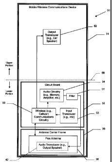
[0023] Referring initially to FIGS. 1 through 9, a mobile
wireless communications device 30 illustratively includes a
portable housing 31, a circuit board 32 (e.g., a printed circuit
board (PCB)) carried by the portable housing, one or more
4
CA 02717402 2010-10-12
wireless communications circuits 33 carried by the circuit
board, and one or more audio circuits 34 carried by the circuit
board. The device 30 further illustratively includes an antenna
assembly 35 including an antenna carrier frame 36 that is
removably coupled to the circuit board 32. More particularly,
the antenna carrier frame 36 is shown coupled to the circuit
board 32 in FIG. 2, and decoupled from the circuit board in FIG.
3. The exemplary device 30 further illustratively includes a
display 60 and a plurality of control keys including an "off
hook" (i.e., initiate phone call) key 61, an "on hook" (i.e.,
discontinue phone call) key 62, a menu key 63, and a return or
escape key 64. Operation of the various device components and
input keys, etc., will be described further below with reference
to FIG. 14.
[0024] As seen in FIG. 6, the antenna carrier frame 36
defines a cavity 37 therein, and a flex antenna 38 is carried on
front (FIG. 7), bottom (FIG. 8), and back (see FIG. 6) surfaces
of the antenna carrier frame 36. That is, the antenna elements
40, 41 may be conceptually considered as "wrap around" antenna
elements which overlie a plurality of different surfaces of the
antenna carrier frame 36 (and a lid 43 therefor, as will be
discussed further below). In the illustrated example, the flex
antenna 38 includes a flexible substrate and a plurality of
capacitively coupled antenna elements 40, 41. In particular, the
antenna element 40 is a folded inverted F antenna, while the
element 41 is a monopole antenna, although a single antenna
element or different combinations of elements (e.g., multiple
monopoles and/or multiple inverted F elements) may be used in
different embodiments.
[0025] As shown in FIG. 4, the antenna element(s) is
electrically coupled to the wireless communications circuit or
circuitry 33, which may comprise one or more cellular
CA 02717402 2010-10-12
transceivers, for example. In the present example, the antenna
elements 40, 41 provide penta-band operation in the GSM 850/950,
DCS, PCS, and UMTS frequency band ranges, as will be appreciated
by those skilled in the art. However, in other embodiments
different numbers and types of frequency bands may be used. For
example, the flex antenna 38 and wireless communications
circuitry 33 may operate over other wireless communications
frequency bands, such as WiFi (e.g., 802.11x, WiMax, Bluetooth),
satellite positioning system bands (e.g., GPS, Galileo, GLONASS,
etc.). In the illustrated embodiment, a separate Bluetooth
antenna 50 is carried on the circuit board 32 (see FIGS. 2 and
3).
[0026] The device 30 further illustratively includes an audio
output transducer 42 carried within the cavity 37 of the antenna
carrier frame 36 and coupled to the audio circuit 34. This
arrangement advantageously conserves scarce surface area or
"real estate" on the circuit board 32, which as may be seen in
FIGS. 2 and 3 is used for other device components. That is, by
co-locating the antenna carrier frame 36 and audio output
transducer 42 in the same vertically overlapping space, this
preserves a significant amount of circuit board 32 space that
may advantageously be used for other components.
[0027] Moreover, in the present embodiment, the audio output
transducer 42 is a loudspeaker, such as for playing music. In
this regard, the audio circuitry 34 may include a data storage
device (e.g., FLASH memory) for storing digital music or audio
files (e.g., MP3, WAV, etc.), a digital-to-analog (D/A)
converter, and an audio output amplifier for outputting the
analog audio signals via the loudspeaker. In some embodiments,
one or more electromagnetic (EM) filter elements 51 (e.g.,
ferrite bead, etc.) may be coupled between the audio circuitry
34 and the audio transducer 42 to avoid undesired interference
6
CA 02717402 2010-10-12
from the antenna elements 40, 41, as will be appreciated by
those skilled in the art. In this regard, depending upon the
given implementation, it may be desirable to route the lead
lines for the audio transducer 42 and/or the antenna elements
40, 41 to avoid high coupling points. Such points will vary
depending upon the given operating frequencies and radiation
patterns of the antenna being used, as will also be appreciated
by those skilled in the art.
[0028] The antenna carrier frame 36 may advantageously
provide an acoustic enclosure for the loudspeaker 42 to enhance
the sound characteristics of the audio output, as will be
appreciated by those skilled in the art. In this regard, a lid
43 may also be provided for the antenna carrier frame 36,to
enclose or encapsulate the audio output transducer within the
cavity 37, as seen in FIG. 6, which not only provides a
proactive covering for the transducer but may also further
advantageously enhance the fidelity of the audio output, as will
also be appreciated by those skilled in the art. The lid 43 also
provides an additional surface (i.e., a back surface) on which
the flex antenna 38 may be overlayed (see FIG. 7), as noted
above. However, it should be noted that in some embodiments the
lid 43 need not be included. The lid 43 and antenna carrier
frame 36 may be made of dielectric materials such as plastic,
although other materials may also be used to provide different
sound enhancement in different embodiments.
[0029] The antenna carrier frame 36 also illustratively
defines an acoustic port 44 therein, in which a speaker gasket
45 is positioned or carried (see FIG. 6). By way of example, the
speaker gasket 45 may comprise a rubber material with a fabric
mesh thereon, although other acoustically suitable materials may
also be used in different embodiments, as will be appreciated by
those skilled in the art. As a result of this configuration, the
7
CA 02717402 2010-10-12
audio output transducer 42 may advantageously be positioned in
relatively close proximity to the lid 43 to provide still
further space savings. In the example illustrated in FIGS. 2 and
3, this spacing is approximately 0.6 mm, although other spacings
may be used in different embodiments.
[0030] In the exemplary wireless phone implementation, the
device 30 further illustratively includes another audio output
transducer 52 carried in an upper portion (or half) of the
portable housing 31, and an audio input transducer 53 carried in
a lower portion (or half) of the portable housing, each of which
is connected to the wireless communications circuitry 33, as
shown in FIG. 4. The upper and lower portions of the portable
housing 31 are separated by an imaginary horizontal centerline
68 in FIG. 4. More particularly, the audio output transducer 52
provides a telephonic ear speaker for a user's ear, and the
audio input transducer 53 provides a microphone for receiving
the user's voice during a phone conversation, as will be
appreciated by those skilled in the art.
[0031] It will therefore be appreciated that the antenna
assembly 35 is positioned in the lower portion (i.e., bottom) of
the portable housing 31. Such placement may advantageously
reduce undesirable coupling of the antenna elements 40, 41 to
other components located at the upper portion (i.e., top) of the
device 30, such as a separate satellite positioning antenna, a
camera circuit 54 (FIG. 4), and/or the output transducer 52,
which may be particularly important to achieve applicable
hearing aid compatibility (HAC) requirements. Moreover,
placement of the antenna assembly 35 in the lower portion of the
housing 31 may also advantageously lower the specific absorption
rate (SAR) of the device 30, since this places the antenna
further away from the user's brain than placement in the upper
portion as found in many traditional cellular phone designs.
8
CA 02717402 2010-10-12
[0032] An exemplary method for using the device 30 is now
described with reference to FIG. 13. As noted above, the audio
output transducer 52 may advantageously be used for playing
audio voice signals, such as during a phone call, and the audio
output transducer 42 may be used for other types of audio output
such as music, etc. Accordingly, the audio output transducer 42
may be designed and constructed to provide a greater volume and
a larger and.flatter frequency range, that is, be of higher
fidelity that the other audio output transducer B52.
[0033] Beginning at Block 130, if the audio output to be
played is not audio voice signals, at Block 131, then this audio
may advantageously be directed to the audio output transducer 42
(Block 132). In some embodiments, even if the audio output
signals to be played are voice signals, they may still
optionally be played on the audio output transducer 42. For
example, the wireless communications circuitry 33 may also be
coupled to the audio circuitry 34, and if the device 30 is in a
hands-free or speakerphone mode (Block 133) then it may be
desirable to instead play the voice audio via the audio output
transducer 42, which may have better audio quality for
relatively high volume applications for the reasons noted above.
However, if the hands-free mode is not chosen, then the voice
audio signals may be played via the audio output transducer 52,
at Block 134, thus illustratively concluding the method of FIG.
13 (Block 135).
[0034] It will be noted that the antenna elements 40, 41 are
closely capacitively coupled in the present example (see FIG.
3), such that these elements operate in an integral fashion in
that the elements would not provide the same coverage patterns
if they were spaced significantly farther apart, even though
these antenna elements have different respective signal feeds
provided via conductive spring connectors 55, 56. A voltage
9
CA 02717402 2010-10-12
reference (e.g., ground) is also provided to the inverted F
antenna 40 via a conductive spring connector 57. In this regard,
a single antenna element could instead be used in some
applications to provide desired multi-band coverage, if desired.
In such cases, the single antenna element may similarly have a
plurality of spaced apart signal feed points thereon coupled to
the wireless communications circuitry 33, such as by the
conductive spring connectors 55, 56. In addition, in some
alternative embodiments an input transducer (e.g., the input
transducer 53) or other devices may be positioned in the cavity
37 of the of the antenna carrier frame 36 in addition to (or
instead of) the transducer 42, as will be appreciated by those
skilled in the art.
[0035] Turning additionally to FIGS. 10-12, an alternative
embodiment of a multi-layer flex antenna 38' is now described.
By way of background, as global 3G (and 4G) cellular deployment
increases, demand for data transmission capacity also increases.
To address such demands, the wireless communication industry
relies on various frequency bands to provide adequate bandwidth
for consumer demands. At present over twenty bands exist ranging
from 704 MHz to 2.7 GHz. A significant challenge to designing a
cellular phone that operates in all of these bands is creating
an antenna that has a large enough bandwidth to transmit or
receive while having sufficient gain at these frequencies, yet
which is compact enough to fit in a relatively small form
factor. As will be discussed further below, the multi-layer flex
antenna 38' advantageously addresses these technical problems by
providing a penta-band main antenna for a mobile wireless
communications device which covers operating frequencies from
824 MHz to 2.17 GHz, for example.
[0036] There are fundamental limits of antennas which may be
understood by considering the entire antenna system including
CA 02717402 2010-10-12
the oscillator, transmission lines, and the antenna itself.
Now, consider a spherical volume with radius r enclosing the
entire structure. The total energy outside the sphere is equal
to the sum of the energies of a given set of current
distribution (called mode hereafter) within the sphere.
[0037] The radiated power of the antenna is calculated from
the propagating modes, while the non-propagating modes
contribute to the reactive power. If the sphere enclosing the
structure is very small, there exist no propagating modes. In
this case, the Q of the system becomes large, and all modes are
evanescent. Much like a resonator, the Q of each mode is defined
as the ratio of energies. In the case of an antenna, Q is
defined as the ratio of its stored energy to its radiated
energy. For propagating modes, Q is given by the following
equation (See Chu, "Physical Limitations of Omnidirectional
Antennas," MIT Technical Report, No.64, May 1948, and McLean, "A
Re-Examination of the Fundamental Limits on the Radiation Q of
Electrically Small Antennas," IEEE Trans. on Ant. and Prop.,
Vol. 44, No. 5, pp. 672-676, May 1996):
1 +2 kr)2
(kr) 3 {1 + f 2 'L 2]
where for kr .1, the expression can be simplified to
1
This expression represents the fundamental limit on the
electrical size of an antenna.
[0038] For a given mode, the fractional bandwidth is
inversely proportional to Q and is given by the following
relationship:
11
CA 02717402 2010-10-12
FBW
Q
For example, within the same spherical volume, a dipole has
kr 0.62, whereas a Goubau antenna has kr 1.04. See Balanis,
"Antenna Theory Analysis and Design," 3rd Ed., John Wiley & Sons,
Inc., Hoboken, New Jersey, 2005. In.other words, the bandwidth
of an antenna (which can be closed within a sphere of radius r)
may be improved only if the antenna utilizes efficiently, with
its geometrical configuration, the available volume within the
sphere.
[0039] The flex antenna 38' design makes use of the above-
described concept. Referring to FIG. 11, one set of modes, say
rl, contributes the radiation for GSM 850, 900, and DCS bands,
while another mode, r2, contributes the radiation for PCS and
UMTS bands, as will be appreciated by those skilled in the art.
For low frequencies, the smallest sphere that encloses the
antenna structure would be affected by the equivalent source
distribution on surface rl as shown. That is, beyond rl, other
modes become evanescent. To create propagating modes in the
region where r is smaller than r1, a different source
distribution is used.
[0040] The flex antenna 38' advantageously uses a multi-layer
structure to accomplish this. The flex antenna 38'
illustratively includes a stack of layers which, from bottom to
top as shown in FIG. 12, are listed along with their respective
thicknesses as follows: a pressure sensitive adhesive (PSA)
layer 70' (50 pm); a polyimide dielectric layer 71' (12 pm); an
adhesive layer 72' (12 pm); a lower conductive (e.g., copper)
layer 73' (12 pm) ; a polyimide spacer layer 74' (16 pm) ; an
upper (e.g., copper) conductive layer 75' (12 pm); an adhesive
12
CA 02717402 2010-10-12
layer 76' (12 pm); and a polyimide layer 77' (12 pm). The
various adhesive and polyimide dielectric layers are
advantageously flexible to allow placement of the flex antenna
38' to accommodate mechanical constraints, yet still provide the
requisite support and protection for the conductive layers 73',
75'.
[0041] By way of example, the PSA layer 70' may be a 3M 9671
LE adhesive transfer tape from the 3M Company of St. Paul., MN.
Moreover, the layer groups 71'/72' and 76'/77' may be obtained
in a combination polyimide/adhesive layer form, such as product
number CVA0515KA from the Arisawa Mfg. Co., Ltd. of Japan.
Furthermore, the copper layers 73', 75' may be implemented with
Teraoka No. 831 from Teraoka Seisakusho Co., Ltd., and an
exemplary intervening polymide layer 74' may be implemented with
Permacel P-221 AMB from Nitto Denko America, Inc. The conductive
layers 73', 75' are patterned (e.g., by etching, etc.) to the
desired geometries before the layers are stacked to form the
flex antenna 38'.
[0042] It should be noted that in different embodiments
various types of suitable adhesive, dielectric spacer, and
conductive materials may be used, as are well know to those
skilled in the electronic circuit arts. Moreover, the
thicknesses and numbers of the various layers may also be
different in different embodiments. For example, in some
embodiments more than two conductive layers may be included in
the stack of dielectric/adhesive/conductive layers.
[0043] The lower conductive layer 73' determines the source
distribution on r2, and the conductive layer 75' determines the
source distribution on rl. In the example illustrated in FIG. 10,
the flex antenna 38' includes feed points 80', 81' which provide
signal and voltage reference (e.g., ground) connection points
for the antenna. In some implementations an additional feed
13
CA 02717402 2010-10-12
point 82' may also be used to provide a second signal feed point
for the antenna 38', such that the single antenna has multiple
signal feed points as described above.
[0044] A related method for making the device 30 may include
positioning the audio circuitry 34 and wireless communications
circuit 33 on the circuit board 32, and positioning the audio
output transducer 42 within the cavity of the antenna carrier
frame 36. The flex antenna assembly 38 is positioned on at least
some of the surfaces of the antenna carrier frame 36, as
discussed above. The method further includes positioning the
circuit board 32 and antenna carrier frame 36 within the
portable housing 31, and electrically coupling the audio output
transducer 42 to the audio circuit 34 and the conductive layers
73', 75' to the wireless communications circuit. Of course, it
will be appreciated by those skilled in the art that some of the
above steps may be performed in different orders in various
embodiments, and that other steps may also be performed (e.g.,
positioning of filter 51, input transducer, output transducer
52, etc.) in various orders depending upon the given
implementation. Moreover, various components may be coupled to
the circuit board 32 after it has already been placed within the
portable housing 31, for example.
[0045] Other exemplary components that may be used in various
embodiments of the above-described mobile wireless
communications device are now described with reference to an
exemplary mobile wireless communications device 1000 shown in
FIG. 14. The device 1000 illustratively includes a housing 1200,
a keypad 1400 and an output device 1600. The output device shown
is a display 1600, which may comprise a full graphic LCD. In
some embodiments, display 1600 may comprise a touch-sensitive
input and output device. Other types of output devices may
alternatively be utilized. A processing device 1800 is contained
14
CA 02717402 2010-10-12
within the housing 1200 and is coupled between the keypad 1400
and the display 1600. The processing device 1800 controls the
operation of the display 1600, as well as the overall operation
of the mobile device 1000, in response to actuation of keys on
the keypad 1400 by the user. In some embodiments, keypad 1400
may comprise a physical keypad or a virtual keypad (e.g., using
a touch-sensitive interface) or both.
[0046] The housing 1200 may be elongated vertically, or may
take on other sizes and shapes (including clamshell housing
structures, for example). The keypad 1400 may include a mode
selection key, or other hardware or software for switching
between text entry and telephony entry.
[0047] In addition to the processing device 1800, other parts
of the mobile device 1000 are shown schematically in FIG. 14.
These include a communications subsystem 1001; a short-range
communications subsystem 1020; the keypad 1400 and the display
1600, along with other input/output devices 1060, 1080, 1100 and
1120; as well as memory devices 1160, 1180 and various other
device subsystems 1201. The mobile device 1000 may comprise a
two-way RF communications device having voice and data
communications capabilities. In addition, the mobile device 1000
may have the capability to communicate with other computer
systems via the Internet.
[0048] Operating system software executed by the processing
device 1800 may be stored in a persistent store, such as the
flash memory 1160, but may be stored in other types of memory
devices, such as a read only memory (ROM) or similar storage
element. In addition, system software, specific device
applications, or parts thereof, may be temporarily loaded into a
volatile store, such as the random access memory (RAM) 1180.
Communications signals received by the mobile device may also be
stored in the RAM 1180.
CA 02717402 2010-10-12
[0049] The processing device 1800, in addition to its
operating system functions, enables execution of software
applications or modules 130OA-1300N on the device 1000, such as
software modules for performing various steps or operations. A
predetermined set of applications that control basic device
operations, such as data and voice communications 1300A and
1300B, may be installed on the device 1000 during manufacture.
In addition, a personal information manager (PIM) application
may be installed during manufacture. The PIM may be capable of
organizing and managing data items, such as e-mail, calendar
events, voice mails, appointments, and task items. The PIM
application may also be capable of sending and receiving data
items via a wireless network 1401. The PIM data items may be
seamlessly integrated, synchronized and updated via the wireless
network 1401 with the device user's corresponding data items
stored or associated with a host computer system.
[0050] Communication functions, including data and voice
communications, are performed through the communications
subsystem 1001, and possibly through the short-range
communications subsystem. The communications subsystem 1001
includes a receiver 1500, a transmitter 1520, and one or more
antennas 1540 and 1560. In addition, the communications
subsystem 1001 also includes a processing module, such as a
digital signal processor (DSP) 1580, and local oscillators (LOs)
1601. The specific design and implementation of the
communications subsystem 1001 is dependent upon the
communications network in which the mobile device 1000 is
intended to operate. For example, a mobile device 1000 may
include a communications subsystem 1001 designed to operate with
the MobitexTM, Data TACTM or General Packet Radio Service (GPRS)
mobile data communications networks, and also designed to
operate with any of a variety of voice communications networks,
16
CA 02717402 2010-10-12
such as AMPS, TDMA, CDMA, WCDMA, PCS, GSM, EDGE, etc. Other
types of data and voice networks, both separate and integrated,
may also be utilized with the mobile device 1000. The mobile
device 1000 may also be compliant with other communications
standards such as GSM, 3G, UMTS, 4G, etc.
[0051] Network access requirements vary depending upon the
type of communication system. For example, in the Mobitex and
DataTAC networks, mobile devices are registered on the network
using a unique personal identification number or PIN associated
with each device. In GPRS networks, however, network access is
associated with a subscriber or user of a device. A GPRS device
therefore utilizes a subscriber identity module, commonly
referred to as a SIM card, in order to operate on a GPRS
network.
[0052] When required network registration or activation
procedures have been completed, the mobile device 1000 may send
and receive communications signals over the communication
network 1401. Signals received from the communications network
1401 by the antenna 1540 are routed to the receiver 1500, which
provides for signal amplification, frequency down conversion,
filtering, channel selection, etc., and may also provide analog
to digital conversion. Analog-to-digital conversion of the
received signal allows the DSP 1580 to perform more complex
communications functions, such as demodulation and decoding. In
a similar manner, signals to be transmitted to the network 1401
are processed (e.g. modulated and encoded) by the DSP 1580 and
are then provided to the transmitter 1520 for digital to analog
conversion, frequency up conversion, filtering, amplification
and transmission to the communication network 1401 (or networks)
via the antenna 1560.
[0053] In addition to processing communications signals, the
DSP 1580 provides for control of the receiver 1500 and the
17
CA 02717402 2010-10-12
transmitter 1520. For example, gains applied to communications
signals.in the receiver 1500 and transmitter 1520 may be
adaptively controlled through automatic gain control algorithms
implemented in the DSP 1580.
[0054] In a data communications mode, a received signal, such
as a text message or web page download, is processed by the
communications subsystem 1001 and is input to the processing
device 1800. The received signal is then further processed by
the processing device 1800 for an output to the display 1600, or
alternatively to some other auxiliary I/O device 1060. A device
user may also compose data items, such as e-mail messages, using
the keypad 1400 and/or some other auxiliary I/O device 1060,
such as a touchpad, a rocker switch, a thumb-wheel, or some
other type of input device. The composed data items may then be
transmitted over the communications network 1401 via the
communications subsystem 1001.
[0055] In a voice communications mode, overall operation of
the device is substantially similar to the data communications
mode, except that received signals are output to a speaker 1100,
and signals for transmission are generated by a microphone 1120.
Alternative voice or audio I/O subsystems, such as a voice
message recording subsystem, may also be implemented on the
device 1000. In addition, the display 1600 may also be utilized
in voice communications mode, for example to display the
identity of a calling party, the duration of a voice call, or
other voice call related information.
[0056] The short-range communications subsystem enables
communication between the mobile device 1000 and other proximate
systems or devices, which need not necessarily be similar
devices. For example, the short-range communications subsystem
may include an infrared device and associated circuits and
components, Near-Field Communication (NFC) or a BluetoothTM
18
CA 02717402 2010-10-12
communications module to provide for communication with
similarly-enabled systems and devices.
[0057] Many modifications and other embodiments will come to
the mind of one skilled in the art having the benefit of the
teachings presented in the foregoing descriptions and the
associated drawings. Therefore, it is understood that the
disclosure is not to be limited to the specific embodiments
disclosed, and that modifications and embodiments are intended
to be included.
19