Note: Descriptions are shown in the official language in which they were submitted.
CA 02718204 2010-10-22
-1-
CONDUCTIVE PASTE FOR FORMING A SOLAR CELL ELECTRODE
BACKGROUND OF THE INVENTION
1. Field of the Invention
[0001] The present invention relates to a fired-type
conductive paste containing glass frit and a conductive
powder comprising silver as a main component and used for
forming a solar cell electrode.
2. Description of the Related Art
[0002] Conventionally, an ordinary solar cell device is
provided with a silicon semiconductor substrate, a
diffusion layer, an antireflective film, a rear electrode
and a front electrode (hereunder sometimes called a
"light-receiving electrode"). When forming the front
electrode in particular, the electrode is formed by screen
printing, stencil printing or the like, using a conductive
paste made by mixing conductive particles composed mainly
of silver with glass frit, an organic vehicle, etc.
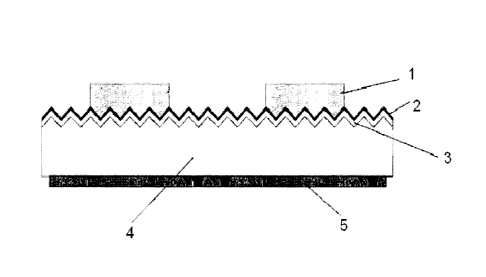
[0003] As one example, in the crystalline silicon solar
cell shown in FIG. 1, a diffusion layer 3 is formed in the
front surface (light-receiving surface) area of a p-type
crystalline silicon substrate 4, which is formed with a
concave-convex surface structure called a textured
structure. The diffusion layer 3, which is formed by
diffusing an impurity such as phosphorus (P) into the
semiconductor substrate 4 from the light-receiving surface
thereof, is a region exhibiting the opposite conductivity
type from the semiconductor substrate 4 (in the present
example, the opposite conductivity type is explained as n-
type). The nLtype diffusion layer 3 is formed for example
CA 02718204 2010-10-22
-2-
by placing the semiconductor substrate 4 in a diffusion
furnace, and heating it in phosphorus oxychloride (P0013)
or the like. An insulating antireflective film 2 is
formed from silicon nitride, silicon oxide, titanium oxide
or the like on this diffusion layer 3 to provide an
antireflective function while at the same time Protecting
the solar cell device. In the case of silicon nitride
(hereunder, "SiN") for example, the film is formed by
plasma CVD or the like using a mixed gas of silane (SiH4)
and ammonia (NH3). The antireflective film 2 is formed
with a thickness of about 5 to 100 nm and a refractive
index of about 1.8 to 2.3, taking into consideration the
difference between this refractive index and that of the
semiconductor substrate 4 and the like.
Next, the aforementioned conductive paste is printed
or coated in a grid form on the antireflective film 2 by
screen printing or the like, and fired at about 500 to
900 C to form a front electrode 1. Normally, electrical
contact between the front electrode 1 and the n-type
diffusion layer 3 is achieved when antireflective film 2
is melted by the action of the glass frit in the
conductive paste and removed during firing. This is
commonly called "fire-through".
A rear electrode 5 is formed on the rear side of the
semiconductor substrate 4 together with a highly
concentrated p-type BSF (Back Surface Field) layer doped
with aluminum or the like.
[0004] To achieve proper fire-through, glasses having
good solubility with the antireflective film 2 have been
preferably used as the glass frit in the conductive pastes.
Among them, especially glass containing lead oxide has
often been used for the glass frit in conventional
conductive pastes for forming front electrodes because the
glass softening point is easy to adjust and the glass
CA 02718204 2010-10-22
-3-
provides good adhesiveness with the substrate (adhesive
strength), allows for relatively good fire-through and
results in superior solar cell characteristics.
For example, lead borosilicate glass frit is used in
the silver pastes for forming solar cell electrodes
described in Japanese Patent Publication Nos. 11-213754 A,
2001-093326 A and 10-326522 A, while Japanese Patent
Publication No. 2001-118425 A describes lead borate glass
frit in addition to lead borosilicate glass frit.
[0005] Regarding the aforementioned fire-through,
however, problems with variation in adhesive strength and
failure to obtain stable ohmic contact between the front
electrode 1 and the n-type diffusion layer 3 of the
semiconductor substrate 4 have occurred when the front
electrode 1 does not penetrate through the antireflective
film 2 due to variation in the effect of the glass frit
and the like when the front electrode 1 is fired.
Insufficient ohmic contact can cause loss during output,
resulting in lower conversion efficiency of the solar cell
and a decline in the current-voltage characteristics.
[0006] As described in paragraph [0004] of Japanese
Patent Publication No. 10-326522 A, paragraph [0017] of
Japanese Patent Publication No. 2004-207493 A, etc,
meanwhile, there has been known another problem in which
excessive fire-through may also Produce inferior voltage
characteristics. Since the antireflective film 2 can be
no more than about 5 to 100 nm thick as described above,
if the front electrode 1 penetrates through the
antireflective film 2 and then through the n-type
diffusion layer 3 below to intrude into the semiconductor
substrate 4, the p-n junction may be broken, and the fill
factor ("FF") obtained from the current-voltage
characteristic measurements may be adversely affected.
Such penetration may become more likely and harder to
CA 02718204 2010-10-22
-4-
control if in the future the n-type diffusion layer 3 is
made still thinner in an effort to improve efficiency.
[0007] FIG. 2 shows the interface between a front
electrode and a semiconductor substrate of a commercial
solar cell substrate as seen through a transmission
electron microscope (TEM). Lead glass is used in the
front electrode of this commercial solar cell. In FIG. 2,
a lead glass layer 6 containing a silver component from
the conductive paste is present between the front
electrode layer la and the SiN layer 2, which is an
antireflective film, and part 7 of this glass layer
penetrates through the SiN layer 2 to contact a silicon
substrate (or n-type diffusion layer) 4, but in part 8
there is too much fire-through, and the glass can be seen
as protrusions intruding deeply into the interior of the
semiconductor substrate 4.
[0008] As a separate issue, increased environmental
awareness in recent years has led to a desire for a
switchover to lead-free materials and parts in solar cells.
Alternative materials and parts are therefore being
developed that will provide ease of adjusting the
softening point of the glass, good adhesiveness to the
substrate (high adhesive strength) and good fire-through,
as in the case of the conventional lead glass, with the
aim of providing superior solar cell characteristics.
[0009] For example, attempts have been made to form
front electrodes using zinc borosilicate glass frit in
Japanese Patent Publication No. 2001-118425 A, bismuth
borosilicate and zinc borosilicate glass frits in Japanese
Patent Publication No. 10-326522 A, borosilicate glass
frit in Japanese Patent Publication No. 2008-543080 A
(Japanese translation of WO 2006/132766) and zinc borate
glass frit in Japanese Patent Publication No. 2009-194121
A. However, the research of the present inventors has
CD, 02718204 2012-12-20
- 5 -
shown that even using such lead-free glass, fire-through .
is sometimes difficult to control, including cases of
insufficient fire-through, failure to achieve ohmic
contact, or, as in FIG. 2, excessive fire-through such
that part of the front electrode intrudes deeply into the
semiconductor substrate.
[0010] On the other hand, tellurium glass is known as a
glass for use in fluorescent display tube sealing
applications (Japanese Patent Publication No. 10-029834 A)
and optical fiber material applications (Japanese Patent
Publication No. 2007-008802 A). In general, tellurium glass
is known to have a low melting point, to be highly durable
and to easily dissolve silver in solid solution, but it also
has extremely low reactivity with silicon oxide, and since
silicon-type antireflective films have been popular in recent
years, there has been little interest in tellurium glass for
forming the front electrodes of solar cells.
SUMMARY OF THE INVENTION
[0011] It is an object of the present invention to provide
a conductive paste for forming a solar cell electrode,
containing no lead, but capable of forming an electrode
providing good solar cell characteristics.
[0012] The present invention comprises the following.
(1) A conductive paste for forming a solar cell
electrode, including: a conductive powder comprising silver
as a main component; glass frit; and an organic vehicle,
wherein the glass frit contains tellurium glass frit having
tellurium oxide as a network-forming component and the
tellurium glass frit contains 25 to 90 mo196 of the tellurium
oxide.
(2) The conductive paste for forming a solar cell
electrode according to (1) above, wherein the tellurium glass
CA 02718204 2012-12-20
- 6 -
frit contains one or more of tungsten oxide and molybdenum
oxide.
(3) The conductive paste for forming a solar cell
electrode according to (2) above, wherein the tellurium glass
frit contains a total of 5 to 60 mol% of one or more of the
tungsten oxide and the molybdenum oxide.
(4) The conductive paste for forming a solar cell
electrode according to (2) or (3) above, wherein the
tellurium glass frit contains one or more of zinc oxide,
bismuth oxide and aluminum oxide.
(5) The conductive paste for forming a solar cell
electrode according to (1) above, wherein the tellurium.glass
frit contains the following components:
tellurium oxide: 25 to 90 mol%
at least one of tungsten oxide and molybdenum oxide:
to 60 mol% in total
zinc oxide: 0 to 50 mol%
bismuth oxide: 0 to 25 mol%
aluminum oxide: 0 to 25 mol%.
(6) The conductive paste for forming a solar cell
electrode according to any one of (1) through (5) above,
wherein the tellurium glass frit is contained in the amount
of 0.1 to 10 parts by weight per 100 parts by weight of the
conductive powder.
[0013] With the present invention, it is possible to
obtain a conductive paste capable of forming a solar cell
electrode with good solar cell characteristics without
containing any lead glass as in the past. By preparing a
solar cell using the conductive paste of the present
invention, it is possible to obtain a solar cell having
performance and characteristics well comparable with or
superior to those of conventional solar cells.
CA 02718204 2010-10-22
-7-
BRIEF DESCRIPTION OF THE DRAWINGS
[0014] FIG. 1 is a diagram of a solar cell device.
[0015] FIG. 2 is a TEM photograph of the interface
between a substrate and a front electrode using
conventional lead glass.
[0016] FIG. 3 is a TEM photograph of the interface
between a substrate and a front electrode using the Te
glass of the present invention.
DETAILED DESCRIPTION OF THE PREFERRED EMBODIMENTS
[0017] One embodiment of the conductive paste and solar
cell device according to the present invention is
explained below, but the scope of the present invention is
not limited thereto.
[0018] The conductive paste of the present invention is
explained first. In the conductive paste of the present
invention, glass frit and a conductive powder comprising
silver as a main component are dispersed in an organic
vehicle. The individual components are explained below.
[0019] The conductive powder is not particularly
limited as long as it contains silver as a main component,
and may have a spherical-, flake- or dendrite-shape or the
like as conventionally used. In addition to pure silver
powder, it is possible to use silver-coated composite
powder having at least a silver layer on the surface
thereof, an alloy comprising silver as a main component,
or the like. The average particle size of the conductive
powder is preferably 0.1 to 10 m. It is also possible to
use a mixture of two or more conductive powders having
different average particle sizes, particle size
distributions, shapes or the like, or a mixture of silver
CA 02718204 2010-10-22
-8-
powder with one or more conductive powders other than
silver. There are no particular limitations on the metals
that can be complexed, alloyed or mixed with the silver
powder as long as the function effects of the present
invention are not adversely affected, and examples include
aluminum, gold, palladium, copper, nickel and the like.
From the standpoint of conductivity however it is
desirable to use pure silver powder.
[0020] The present invention is characterized in that
tellurium glass comprising tellurium oxide as a network-
forming component is used as glass frit in the electrode-
forming conductive paste. The conductive paste of the
present invention is especially suited to forming the
electrode on the front surface (light-receiving surface)
of a solar cell, and an electrode providing superior solar
cell characteristics can be obtained by printing this
paste onto an antireflective film of silicon nitride, etc.,
on a solar cell surface and firing it.
[0021] In the tellurium glass (hereunder "Te glass")
used in the present invention, tellurium oxide does not
form glass by itself but is a network-forming component
forming the principal structure of glass, and the content
thereof is 25 to 90 mol% (as oxide) with respect to the
total of the glass frit. When this content is below 25
mol% or above 90 mol% vitrification becomes difficult. The
content range is preferably from 30 to 80 mol% and more
preferably from 40 to 70 mol%.
[0022] The research of the present inventors has shown
that when the conductive paste containing Te glass is used
to form the front electrode of a solar cell, there is
almost no deep penetration into the semiconductor
substrate by the front electrode as shown in FIG. 2, fire-
through is easy to control, and sufficient ohmic contact
can be obtained.
CA 02718204 2010-10-22
-9-
[0023] FIG. 3 shows the interface between a silicon
substrate and a front electrode formed using the
conductive paste of the present invention as observed
under a transmission electron microscope (TEM). A unique
structure is formed in which a Te glass layer 9 comprising
a silver component and a silicon oxide layer 10 with a
series of precipitated fine silver particles 11 are
present between a front electrode layer la and a SiN layer
2. The inventors assume that this is due to the low
reactivity of Te glass with silicon oxide and the property
of Te glass of dissolving silver very easily in solid
solution. Due to the properties of Te glass, it is
believed that large quantities of silver is dissolved as
ions in the Te glass during firing when the electrode is
formed and the silver ions thus dissolved in the glass
subsequently diffuse gradually into the SiN layer 2 via
the glass layer, promoting an oxidation-reduction reaction
that converts part of the surface layer of the SiN layer
into silicon oxide at the interface with the electrode,
while precipitating as very fine silver particles.
Further, since there is no deep penetration into the
silicon substrate 4 even when the electrode does break
through the antireflective film, the conductive paste of
the present invention has a low dependence on firing
temperature compared with conventional conductive paste
and allow for an easy fire-through control and further
reduction in the thickness of the solar cell and further
reduction in the thickness of the n-type diffusion layer,
which are expected to be needed in the future, can be
achieved.
[0024] In the Te glass of the present invention
tellurium oxide is a network-forming component that forms
the network of the glass, and it is also desirable to
include one or more of tungsten oxide and molybdenum oxide
CA 02718204 2010-10-22
-10-
as a component that assists in glass network formation in
addition to tellurium oxide.
[0025] Tungsten oxide and molybdenum oxide both
contribute to expanding the vitrification range of the Te
glass and stabilizing the glass. Vitrification is
difficult if the combined content of these components as
oxides is less than 5 mol% or more than 60 mol%. The
preferred range is 10 to 50 mol%.
[0026] One or more of zinc, bismuth and aluminum are
preferably included in the Te glass of the present
invention, and it is especially desirable to include these
in combination with tungsten and/or molybdenum.
[0027] Zinc helps to expand the vitrification range and
stabilize the glass, but vitrification becomes difficult
if the content thereof as oxide exceeds 50 mol%. The
preferred range is 5 to 30 mol%.
[0028] Bismuth helps to expand the vitrification range
and improve chemical durability, but a crystal phase is
likely to form if the content thereof as oxide exceeds 25
mol%, detracting from the stability of the glass. The
preferred range is 0.5 to 22 mol%.
[0029] Aluminum helps to improve the chemical
durability of the glass, but when the addition thereof as
oxide is above 25 mol%, a significant effect by the
addition cannot be obtained. The preferred range is 2 to
20 mol%.
[0030] In addition, the alkali metal elements such as
lithium and sodium, the alkali earth metal elements such
as magnesium, calcium, strontium and barium and the other
elements such as dysprosium, yttrium, niobium, lanthanum,
silver, zirconium, titanium, boron, germanium, phosphorus
and tantalum can be included alone or in combination
thereof in the Te glass of the present invention in order
to adjust reactivity with the SiN layer and the solid
CA 02718204 2010-10-22
-11-
dissolution amount of silver, and the total content of
these as oxides is preferably 50 mol% or less.
[0031] Further, the Te glass of the present invention
preferably has a softening point of 300 to 550 C. If the
softening point is below 300 C fire-through occurs more
easily, and the front electrode may penetrate through not
only the SiN layer but also the n-type diffusion layer,
increasing the risk of breaking the p-n junction. If the
softening point exceeds 550 C, insufficient glass is
supplied to the junction interface between the front
electrode and the antireflective film, so that the
aforementioned unique structure is not obtained, ohmic
contact is impaired, and the adhesive strength of the
electrode is diminished.
[0032] In addition to the aforementioned Te glass frit,
glass frit other than the Te glass can be combined in the
conductive paste of the present invention. For purposes
of controlling the firing temperature, reactivity to the
SiN layer and the like and controlling the characteristics
of the resulting solar cell device, glass chosen from
among known glasses such as Si07-B203 glass, Si02-B203-ZnO
glass, Si02-Bi203 glass, B203-ZnO glass, etc. can be
combined with the Te glass as appropriate as the glass
frit other than the Te glass, and it is especially
desirable to include Si02-B203 glass or Si02-B203-ZnO glass.
[0033] The glass frit in the conductive paste of the
present invention can be contained in an amount normally
contained in conductive paste for forming solar cell
electrodes, but for example 0.1 to 10 parts by weight per
100 parts by weight of conductive powder is preferred. If
the amount of glass frit is less than 0.1 parts by weight
per 100 parts by weight of conductive powder, adhesiveness
and electrode strength will be very low. If it exceeds 10
parts by weight, on the other hand, there will be problems
CA 02718204 2010-10-22
-12-
with glass float on the electrode surface and increased
contact resistance due to glass flowing into the interface.
In conventional conductive pastes for forming solar cell
electrodes, a certain amount of glass frit must be added
in order to achieve good fire-through. However, in the
conductive paste of the present invention even when the
amount of glass frit is suppressed, sufficient ohmic
contact can be achieved. A more desirable amount of glass
frit is 0.1 to 5 parts by weight per 100 parts by weight
of conductive powder.
[0034] The average particle size of the glass frit
added in the conductive paste of the present invention is
not particularly limited but is preferably 0.5 to 5.0 m.
[0035] The conductive paste of the present invention
essentially contains no lead component, and specifically
the lead content of the conductive paste is 1000 ppm or
less.
[0036] One or more of plasticizers, viscosity adjusters,
surfactants, oxidizers, metal oxides, organic metal
compounds and the like commonly used as additives can be
added as necessary in the conductive paste of the present
invention to the extent that they do not detract from the
effects of the present invention. The silver compound
such as silver carbonate, silver oxide or silver acetate
described in Japanese Patent Publication No. 2007-242912 A
filed by the applicant can also be added, and one or more
of copper oxide, zinc oxide, titanium oxide and the like
can also be added appropriately in order to control the
firing temperature, improve solar cell characteristics and
the like.
[0037] The conductive paste of the present invention is
formed by mixing the aforementioned conductive powder,
glass frit and appropriate additives together with an
organic vehicle to obtain a paste, paint or ink with a
CA 02718204 2010-10-22
-13-
rheology suited to screen printing or other printing
method. The organic vehicle is not particularly limited,
and an organic binder, solvent, etc. commonly used as a
vehicle in silver paste can be selected and mixed as
appropriate. Examples of organic binders include
celluloses, acrylic resins, phenol resins, alkyd resins,
rosin esters and the like, while examples of solvents
include alcohols, ethers, esters, hydrocarbons and other
organic solvents as well as water and mixed solvents of
these. The amount of the organic vehicle is not
particularly limited, and can be adjusted appropriately
according to the application method to an amount suitable
for retaining inorganic components such as the conductive
powder and the glass frit in a paste, but is normally
about 5 to 40 parts by weight per 100 parts by weight of
the conductive powder.
[0038] The solar cell device in which the conductive
paste of the present invention is used is manufactured for
example as follows.
The semiconductor substrate is preferably of
monocrystalline silicon or polycrystalline silicon, doped
with boron or the like so that the substrate exhibits one
conductivity type (p-type for example). A diffusion layer
is formed by diffusing phosphorus atoms or the like into
the semiconductor substrate from the light-receiving
surface thereof, thereby forming a region exhibiting the
opposite conductivity type (n-type for example), on which
is provided an antireflective film of silicon nitride or
the like. An aluminum paste, silver paste or silver-
aluminum paste is applied onto the substrate surface
opposite the light-receiving surface and dried to form a
rear electrode and a high-concentration p-type BSF layer.
The conductive paste of the present invention is then
applied onto the aforementioned antireflective film by a
CA 02718204 2010-10-22
-14-
conventional method such as screen printing, dried and
fired for a total firing time of about 1 to 30 minutes at
a peak temperature of 500 to 900 C to decompose and remove
the organic vehicle components and simultaneously form the
front electrode, rear electrode and BSF layer. The front
electrode and rear electrode do not have to be co-fired,
and the front electrode can be formed after the rear
electrode is fired, or the rear electrode can be formed
after the front electrode is fired. The light-receiving
surface of the semiconductor substrate preferably has a
textured structure with a concave-convex surface (or
pyramid-like asperities) in order to obtain better
photoelectric conversion efficiency.
Examples
[0039] The present invention is explained in detail
below by means of examples, but the present invention is
not limited thereby.
1. Preliminary test
[0040] Preparation of Samples 1 to 11
100 parts by weight of silver powder and 2 parts by
weight of glass frit having the compositions shown in
Table 1 were dispersed together in an organic vehicle
composed of 1.6 parts by weight of ethyl cellulose and 6.4
parts by weight of butyl carbitol, to prepare conductive
pastes (Samples 1 to 11). The ingredients in the glass
compositions shown in the table are all given in mol% as
oxides.
[0041] The powders listed in the "silver powder"
columns in the table are as follows. The average particle
size D50 shown below corresponds to a weight-based
cumulative 50% value in particle size distribution as
measured with a laser diffraction particle size analyzer.
Silver powder X: Spherical powder,
CA 02718204 2010-10-22
-15-
average particle size D50 = 1.8 pm
Silver powder Y: Spherical powder,
average particle size D50 = 1.5 pm
Silver powder Z: Spherical powder,
average particle size D50 = 2.6 pm
Electrode formation and evaluation
For initial evaluation of the conductive pastes thus
prepared, contact resistance was measured as follows by
the TLM (transmission line model) method.
[0042] First, 10 of 2 cm x 2 cm square-shaped p-type
silicon substrates with a pyramidal texture formed by
alkali etching were prepared for each sample, phosphorus
was diffused into each substrate from one principal
surface (light-receiving surface) to form an n-type region
(diffusion layer), and an SiN layer was formed thereon by
plasma CVD to an average thickness of 75 nm.
Next, a plurality of front electrodes in the form of
fine line 100 m wide and 15 m thick were formed on the
SiN layer with a pitch of 2 mm between the line-shaped
electrode, using Samples 1 to 11 prepared above, the
resistance value between the line-shaped electrodes was
measured with a digital multimeter (3458A Multimeter made
by Hewlett Packard Co.), and the contact resistance was
determined and used to evaluate the samples.
Note that the front electrodes were fired at a peak
temperature of 800 C.
[0043] The results are shown together in Table 1. The
symbols used in the "contact resistance" columns in the
table are as follows.
Average contact resistance for 10 substrates is
less than 0.05 f2cm2
CD Average contact resistance for 10 substrates is
at least 0.05 Qcm2 but less than 0.08 Qcm2
Average contact resistance for 10 substrates is
CA 02718204 2010-10-22
-16-
at least 0.08 Qcm2 but less than 0.10 Qcm2
X Average contact resistance for 10 substrates is
0.10 Qcm2 or more
Next, the interface between the front electrode and
the silicon substrate was observed in a TEM photograph, as
described above, and penetration by the front electrode
through the SiN layer into the silicon substrate was
evaluated as follows. The results are shown in the
"penetration" column in the table.
A: Maximum penetration through the SiN layer into the
silicon substrate is less than 100 nm.
B: Maximum penetration is at least 100 nm but less than
200 nm.
C: Maximum penetration is at least 200 nm but less than
300 nm.
D: Maximum penetration is 300 nm or more.
As discussed above, when the Te glass is used for the
glass frit in the conductive paste, generally good contact
resistance is obtained as shown in Table 1
Table 1
Ag Glass composition Contact
Sample Penetration
powder Te W Mo Bi resistance
1 X 40.0 50.0 = 10.0 A 0
2 X 50.0 40.0 10.0 A
0 0
3 X 60.0 20.0 20.0 A
0
1.)
4 X 60.0 25.0 15.0 A
0 ..3
1-,
co
X 60.0 30.0 10.0 A
1 1.)
,
00.
1--,
6 X 70.0 20.0 10.0 B 0
I
o
7 X 50.0 40.0 10.0 A 0
1-,
0
8 X 60.0 20.0 20.0 A
1
1-,
0
9 X 60.0 30.0 10.0 A 0
1
1.)
1.)
X 60.0 35.0 5.0 A 0
11 X 70.0 20.0 10.0 B 0
CA 02718204 2010-10-22
-18-
Evaluation of Samples 12-81
[0044] Samples 12 to 81 were prepared as in Samples 1
to 11 except that the glass compositions and silver
powders contained in the conductive pastes were changed as
given in Table 2-1 and Table 2-2 and their contact
resistances were measured and evaluated as in Samples 1 to
11. The results are shown in Table 2-1 and Table 2-2.
The respective ingredients of the glass compositions are
all given in mol% as oxides in the tables.
Table 2-1
Sam- Ag Glass composition
Pene= Contact
ple powder_ Te W Zn Mo Bi 4 Al Ag B
Zr P Ti Li _ Mg Ta Nb Ba La Dy Y Si Cu Pb tration resistance
12 X 66.7 28.5 4.8
B 0
_ .
_
13 X 50,0 25.0 25.0
A 0
_. , , .
14 X 50.0 25.0 25.0
A 0
15 X 50.0 25.0 25.0
B 0
. _
16 X 60.0 30.0_ _
10.0 A 0
,
. ,-
17 X _ 70.0 20Ø.
10.0 B 0
18 X 50.0 25.025.0
A 0
. _
19 X 60.0 30.010.0
A 0
. .
, .
20 X 70.0 20.0 10.0
B 4 0 0
21 X 60.0 30.0
410.0 A 0 P
- _ _
_ _ _
22 X 70.0 20.0,
N 10.0 B 0 o )
_ _
23 X50.0 25.0 25.0
A 0 -4
H
_
- , - _
24 X 70.0 20.0 10.0
B 0 co
N)
o
25 X 50.0 25Ø . I 25.0 A
0 o= , _
26 Y 40.0 20.0 6.7 33.3
B @
. .
_
. _
L_O o
0
27 X 50.0 40.0
A 0 I H
10.0
.
-
I
28 Y 50.0 25.0 8.3 16.7
B @
. ,
H
29 Y 54.5 27.3 9.1. 9.1
A C) 0
1
30 Y 54.5 27.3 9.1 9.1 4
B 0
_ rs)
_ . _
N)
31 Y 54.5 27.3 9.1 4 9.1
B 0
32 X 55.8 32.5 4.7 2.3 4.7
B 0
._
33 Y 55.8 27.9 9.3. _ . ,
..
, 7.0 A 0
, _
34 Y 57.1 28.6 9 4
A 0
.5.8 _ . .
_ _
35 Y _57.1 28.6 9.5 4.8B
@
. -
36 Y 57.1 28.6 9.5 4 4.8
B 0
_ _
37 Y 58.0 29.0 9.6 3 _ . .4 ,
A 0
_
38 Y 58.3 29.1 9 _ .
.7 2.9 B @
. _
-
39 Y 58.5 29.3 9.8 2.4
A @
. _
40 Y 58.5 29.3 9.8 2.4 ,
A @
41 Y 58.5 29.3 9.8 2.4
B @ .
_
- -
42 Y 58.8 29.4 9.8
2.0 B
'
43 X 60.0 25.0 15.0
A @
44 Y 60.0 25.0 15.0
A 0
45 X 60.0 ' 30.0 10.0
' A 0
46 Y 60.0 30.0 10.0 '
. A 0
47 X 65.1 18.6 9.3 2.3 4.7,
B 0
Table 2-2
San = Ag Glass composition
Pene- Contact
ple powder Te W Zn Mo Bi Al _ Ag 13 ,
Zr , P , Ti Li õ Mg Ta _ N1:1 Ba La Dy Y Si Cu Pb tration
resistance
48 Y 65.1 23.2 - i
4.7 _ 2.3 4.7 . _ B 0
. - . _ _ .
_
49 X 68.3 19.5 9.8 2.4
B 0
- . . , .
_
50 Y 40.0 20.0 6.7
33.3 B 0
_
_ . . . _ _ . _
-
51 Y 46.7 13.3 6.7 33.3_ _
B ,
. . _ _
.
52 X 55.8 _ 27.9 9.3 2.3 4.7
B 0
_
. _ - . -
53 Y 55.8 27.9 9.3 2.3 4.7
B
_
- . , _ ,
54 Y 58.3 16.7 8.3
16.7 B @
_
õ . _ _ , _ ,
55 Y 60.0 30.0 10.0 õ
A ID
_
_ . . .
56 Y 63.6_ 18.2 9.1 ,
9.1 B 0 0
_ _
_ - _
57 Y 40.0 20.0 20.0 20,0
A 0
_ ,
_
_ _ _ _ . _
-
58 Y 50.0 30.0 _ 10.0 10.0
B 0 o
n.)
_
--3
59 Y 60.0 _ _ 20.0 , 10.0
10.0 B 0
_ _ _ _ .
60 Y 60.0 _25.0 5.0
10.0B , 0 n.)
_ , .
_ o
61 Y 31.7 _ 15.9 _15.931.7 1.6 3.2
B o.
_
- .
i
62 Y 33,3 _ 16.7 16.733.3
B 0 N.) N)
_ _
63 Y 37.2 _ . _37.2 18.6 2.3 4.7
B 0
_ _ . .
_ o
64 Y 41.7 20.8 20.8 16,7
e 1
, ) , 1
1-,
65 Y 41.8 32.6 18.6 2.3 4.7
r r . B 0 0
1
,
66 X 44.5 _. 22.2 22.2 4.4 _2.3
4.4. B 0
_ . n.)
_
n.)
67 X 45.3 22.6 22.6 _ 2.7 2.3 4.5
B 0
_ .
68 X 45.5 22.7 22.7
9.1 B 0
. . . _ -
-
69 Y 45.5 ., 22.7 22.7 9.1
A CI
- .. ,
-
. -
_
70 X 45.5 22.7 22.7 9.1
B 0
. . ,
71 X 45.5 22.7 22.7, 9.1
B 0
. . . I I
72 X 47.6_23.8 23.8 4.8
B 0
. .
t .
. . . .
73 X x 48.8 , 24.4 24.4 2.4
B
. I .
i
74 X 46.2 23.0 23.0 0.9 2.3 4.6
B 0
,
75 , X 46.4 23.3 23.3 2.3 4.7
B 0
76 Y 46.5 37.2 9.3 2.3 4.7
B 0
77 X 47.6 23.8 23.8
4.8 A 0
78 X 50.0 25.0 25.0 ' '
. ,
A 0
79 Y 50.0 25.0 25.0
A 0
-
80 : Z -50.0 ' 25.0 ' 25.0 . '
A 0
81 Y 51.1 32.6 9.3 2.3 4.7
B 0
CA 02718204 2010-10-22
-21-
Evaluation of Samples 82-130
[0045] Samples 82 to 130 were prepared as in Samples 1
to 11 except that the glass compositions and silver
powders contained in the conductive pastes and the part(s)
(by weight) of the glass added to the conductive pastes
were changed as given in Table 3-1 and Table 3-2 and their
contact resistances were measured and evaluated as in
Samples 1 to 11. The results are shown in Table 3-1 and
Table 3-2.
Evaluation of Comparative Samples 1-2
[0046] As Comparative Samples 1 and 2, conductive
pastes were prepared as in Samples 1 to 11 except that the
compositions and amounts of the added glass frits and the
used silver powders were changed as given in Table 3-2 and
their contact resistances were measured and evaluated as
described above. The results are shown in Table 3-2.
[0047] In Tables 3-1 and 3-2, the part or parts of
glass are given part or parts by weight per 100 parts by
weight of silver powder and the respective ingredients of
the glass compositions are all given in mol% as oxides.
Table 3-1
Ag Glass Glass composition
Contact
Sam
Pene=
pow. part(s) by
resis=
ple
Te W Zn Mo Bi Al Ag B Zr P Ti Li Mg Ta Nb Ba La Dy Y Si
Cu Pb tration
der weight
tance
,
,
82 X 0.5 part 46.4 23.3 23.3
2.3 4.7 B 0
-
83 Y 2.5 parts 46.4 23.3 23.3
2.3 4.7 A 0
84 Z 2.5 parts 46.4 23.3 23.3
2.3 4.7 A 0
-
-
85 X
1.5 parts 50.0 26.0 25.0- A 0
.
86 Y
1.5 parts 50.0 25.0 25Ø _ A
- -
87 Z
1.5 parts 50.0 25.0 25.0 A 0
88 Y
3 parts 50.0 25.0 25.0 A 0
-
_
89 Y 1 part 40.0 20.0
6.7 33.3 B 0
90 Y 1 part 50.0 25.0
8.3 16.7 , B 0 (-)
91 Y 1 part 54.5 _ 27.3
9.1 ., 9.1 B 0
,
. -
o
92 Y 1 part 64.6 27.3
9.1 9.1 B 0 t..)
93 Y 1.5 parts 54.5 27.3 9.1
9.1 A 0
.,
_ . _ ...
co
94 Y 1.5 parts 54.5 27.3
9.1 9.1 A C) t..)
95 Y 1.5 parts 54.5 ,27.3
9.1 , 9.1 , B 0 I o.
. . . -
Iv
96 Y 1 part 57.1 28.6 9.5
4.8 B 0 t..)
.
97 _ Y 1 part 57.1 _28.6 9.5 _
4.8 , B 0 I o
i-,
98 Y 1 part
57.1 28.6- 9.5 4.8 B 0 o
1
. -
99 Y 1.5 parts 57.1 28.6 9.5
4.8 A 0 0
-
,
1
100 Y 1.5 parts 57.1 28.6 9.5 _
4.8 B 0 t..)
.
101 Y 1.5 parts 57.1 28.6 9.6
4.8 B 0 t..)
-
102 Y 1.5 parts 57.1 _28.6 _ 9.5
4.8 B 0
,
-
103 Y 1.5 parts 57.1 28.6
9.5 4.8 A _ 0
. . -
104 Y 1.5 parts 57.1 _28.6
9.5 4.8 B 0
._ .
105 Y 1.5 parts 58.3 29.1 9.7
2.9 A 0
..
.
106 Y 1.5 parts 58.3 29.1
9.7 ,._ 2.9- B
107 Y 1 part 58.5 29.3
9.8 2.4 B 0
Table 3-2
Ag Glass Glass composition
Contact
Sam=
Pene-
pow- part(s) by
resis-
ple
Te W Zn Mo Bi Al Ag B Zr P Ti Li Mg Ta Nb Ba La lly Y Si
Cu Pb tration
tance
der weight
.
-
108 Y 1 part 58.5 29.3 _
9.8 2.4- B 0
-
109 Y 1 part ., 58.5 . 29.3
9.8 . 2.4s 0
. .,
110 Y 1.5 parts _58.6 29.3
_ 9.8 _2.4 A 0
111 Y 1.5 parts 58.5 29.3
9.8 2.4' B 0
_
. .
_
. .
112 . Y 1.6 parts 58.5 29.3 9.82.4
B 0
. .
. . .
113 Y 1.5 parts _ 59.4 .29.7
9.9 . . 1.0 e 0
_ _.,
. ,
114 Y 1.5 parts 59.4 29.7 9.9
1.0 A 0
_
. . _
115 Y 1.5 parts 59.4 29.7 9.9
1.0 B 0
116 Y 1.5 parts 59.4 29.7 ,
9.9 1.0 A 0
0
117 Y 1.5 parts 59.6 29.9 _ 10.0- -
. 0.5 A 0
-
118 Y 1.5 parts 59.6 29.9 10.0
0.5 A 0 0
_ _ - , -
n.)
,
-
-
119 X 1 part 60.0 30.0
10.0 B 0 ....]
'
- - _
i-,
120 X 1.5 parts 60.0 30.0
10Ø A 0 co
-
_ - . .
, n.)
_ 121 Y _ 1 part 60.0 _30.0
. 10Ø B 0 I 0
- . .
. -
122 Y 1.5 parts 60.0 30.0 10,0
.
A
..
..
(_,O n.)
. 123 Y 1 part 60.0 25.0
15.0 s 1 0
_ . ,
1-,
124 Y 1.6 parts 60.0 25.0
15.0 A 0 0
1 _ -
125 Y 1.5 parts 40.0 20.0 . 6.7
33 .. .3 B 0 i-
. . . .
. 13 ,
. -
126 Y 1.5 parts 60.0 25.0
8.3 10.7 . 0 I
. - - r- _ -
o
n.)
,
127 X 1 part 60.0
30.0 10.0 B 0 n.)
,
,
128 X 1.5 parts 60,0
30,0 10.0 _. .
A _
. -
129 Y 1 part 60.0
30.0 _., 10.0 s ci
-
.
.
130 Y 1.5 parts 60.0
. . 30.0 ._ 10.0 A 0
-
-
Comp.
Sam- Y 3 parts
2.0 38.0 60.0 C C)
ple 1
,
.
.
. . . .
Comp.
Sam- Y 2 parts 20.0
60.0 20.0 D A
pie 2
CA 02718204 2010-10-22
-24-
[0048] As clear from the above tables, the electrodes
formed using the conductive Pastes of the present
invention provided a low contact resistance therebetween,
without causing penetration through the SiN layer by the
electrode layer and deep penetration into the silicon
substrate. In the case of the front electrodes formed by
the comparative samples, it was confirmed that part of the
electrodes penetrated through the SiN layer and intruded
deeply into the semiconductor substrate.
2. Evaluation of solar cell device characteristics
[0049] As in the preliminary test, an n-type diffusion
layer and a SiN layer were formed in that order on one
principal surface (light-receiving surface) of a 2 cm x 2
cm p-type silicon substrate with a pyramidal textured
structure formed by alkali etching, and a rear electrode
was formed with an aluminum paste onto the rear surface of
the substrate on the opposite side, after which a comb-
shaped pattern was printed on the SiN layer using each of
the aforementioned Samples 44, 79, 88 and 123 so as to
obtain a comb-shaped front electrode (line width: 100 m,
thickness: 15 m, pitch between lines: 2 mm) after firing,
and was fired at a peak temperature of 800 C to form the
front electrode and prepare a solar cell device. The same
samples were also used to form comb-shaped patterns which
were fired at peak temperatures of 760 C and 780 C to
prepare solar cell devices different only in terms of
firing temperature.
[0050] Comb-shaped patterns were also formed with
Comparative Samples 1 and 2, and fired at a peak
temperature of 800 C to prepare solar cell devices.
[0051] The resulting solar cell devices were subjected
to I-V curve measurement using a solar simulator (WXS-50S-
1.5, AM 1.5 G made by WACOM ELECTRIC Co., Ltd.) and high-
current source meter (Model 2400 made by KEITHLEY
CA 02718204 2010-10-22
-25-
INSTRUMENTS, INC.) to determine the open circuit voltage
(Voc), short-circuit current density (Jsc), fill factor
(FF), maximum power output (Pmax) and conversion
efficiency (Eff), with the results shown in Table 4.
Table 4
Glass Firing
Ag Glass composition Voc Jsc
Pmax Eff
Sample part(s) by temper-
FT'
powder [V]
[mA=cm-2l [mWi [%l
weight _________________________________________________________ ature
Te W Zn Bi B Si Pb .
7G0 C 0.608 34.83 0.727 61.61 15.40
44 Y 2 parts 60.0 25.0 15.0 780 C
0.603 34.19 0.717 59.11 14.78
800 C
0.594 _ 30.37 0.724 52.26 13.07
760 C
0.604 32.39 0.758 = 59.31 14.83
123 Y 1 part 60.0 25.0 15.0 780 C
0.600 31.98 0.763 58.53 14.63 (-)
800 C 0.600 32.35 0.761 59.10 14.77
.
.. .._
1..)
760 C 0.605 32.58 0.766 60.38 15.10
--.1
I- '
79 Y 2 parts 50.0 25.0 25.0 780 C
0.603 32.30 0.776 , 60.46 15.11 co
1..)
1
0
800 C 0.605 31.57 0.774 59.14 14.78
760 C 0.603 32.32 0.756 58.89 14.72
I 0
1-.
88 Y 3 parts 50.0 25.0 25.0 780 C
0.604 32.39 0.758 59.31 14.83 0
1
1-.
800 C 0.606 32.56 0.766 60.45 15.11
0
1
1..)
Comp.
"
Sam- Y 3 parts 2.0 38.0 60.0
800 C 0.606 32.98 0.770 61.56 15.39
ple 1
. -
Comp.
Sam- Y 2 parts 20.0 60.0 20.0 800 C
0.593 32.17 0.593 45.24 11.31
ple 2
CA 02718204 2010-10-22
-27-
[0052] It is confirmed
that the solar cell devices
provided with the front electrodes formed by the
conductive pastes of the present invention have low
dependency on firing temperature, as well as excellent
solar cell characteristics.
CA 02718204 2010-10-22
-28-
Explanation of Reference Numerals in Drawings
1 Front electrode
la Front electrode layer
2 Antireflective film or SiN layer
3 Diffusion layer
4 Substrate
Rear electrode
6, 9 Glass layer
Silicon oxide layer
11 Silver particle