Note: Descriptions are shown in the official language in which they were submitted.
CA 02718272 2010-09-10
WO 2009/120340 PCT/US2009/001874
i PROVED JUNCTIONS IN SUBSTRATE SOLAR CELLS
CROSS REFERENCE TO RELATED APPLICATIONS
[0001] This application claims priority to U.S. Provisional Patent Application
Serial No.
61/070,903 filed March 26, 2008 the contents of which is incorporated herein
by
reference.
BACKGROUND OF THE INVENTION
[0002] Increasing oil prices have heightened the importance of developing cost
effective
renewable energy. Significant efforts are underway around the world to develop
cost
effective solar cells to harvest solar energy. In order for solar cells to be
cost effective
with traditional sources of energy solar cells must be manufactured at a cost
well below
$1 /watt.
[0003] Current solar energy technologies can be broadly categorized as
crystalline silicon
and thin film technologies. Approximately 90% of the solar cells are made from
silicon -
single crystal silicon or polycrystalline silicon. Crystalline silicon (c-Si)
has been used as
the light-absorbing semiconductor in most solar cells, even though it is a
relatively poor
absorber of light and requires a considerable thickness (several hundred
microns) of
material. Nevertheless, it has proved convenient because it yields stable
solar modules
with good efficiencies (13-18%, half to two-thirds of the theoretical maximum)
and uses
process technology developed from the knowledge base of the microelectronics
industry.
Silicon solar cells are very expensive with manufacturing cost above
$3.50/watt.
[0004] Second generation solar cell technology is based on thin films. Main
thin film
technologies are Amorphous Silicon, Copper Indium Gallium Selenide (CIGS), and
Cadmium Telluride (CdTe).
1
CA 02718272 2010-09-10
WO 2009/120340 PCT/US2009/001874
[0005] Amorphous silicon (a-Si) was viewed as the "only" thin film PV material
in the
1980s. But by the end of that decade, and in the early 1990s, it was written
off by many
observers for its low efficiencies and instability. However, amorphous silicon
technology
has made good progress toward developing a very sophisticated solution to
these
problems: multijunction configurations. Now, commercial, multijunction a-Si
modules in
the 7-9% efficiency range are being produced by several companies. A number of
companies such as Kaneka, Sharp, Schott Solar, Ersol, etc., are manufacturing
amorphous silicon solar cells on glass substrates by adopting commercially
proven CVD
process to deposit a-Si originally developed for flat panel display
manufacturing.
Equipment companies such as Applied Materials are offering turn-key systems to
manufacture a-Si solar cells on glass substrates. The key obstacles to a-Si
technology are
low efficiencies, light-induced efficiency degradation (which requires more
complicated
cell designs such as multiple junctions), and process costs (fabrication
methods are
vacuum-based and fairly slow). United Solar has pioneered triple junction a-Si
solar cells
on flexible stainless steel substrates. However, a-Si solar cells are
expensive to
manufacture (>$2.5/watt).
[0006] Thin film solar cells made from Copper Indium Gallium Diselenide (CIGS)
absorbers show promise in achieving high conversion efficiencies of 10-12%.
The record
high efficiency of CIGS solar cells (19.9% NREL) is by far the highest
compared with
those achieved by other thin film technologies. These record breaking small
area devices
have been fabricated using vacuum evaporation techniques which are capital
intensive
and quite costly. A number of companies (Honda, Showa Shell, Wurth Solar,
Nanosolar,
Miasole etc.) are developing CIGS solar cells on glass substrates and flexible
substrates.
2
CA 02718272 2010-09-10
WO 2009/120340 PCT/US2009/001874
However, it is very challenging to fabricate CIGS thin films of uniform
composition on
large area substrates. This limitation also affects the process yield, which
are generally
quite low. Because of these limitations, implementation of evaporation
techniques has not
been successful for large-scale, low-cost commercial production of CIGS solar
cells. It is
extremely unlikely that CIGS solar cells can be produced below $1/watt
manufacturing
cost.
[0007] CdTe thin film solar cells are very simple to make and have the
potential to
achieve lowest manufacturing cost compared to all other solar cell
technologies. CdTe
solar cells with 16.5% efficiency have been demonstrated by NREL. First Solar
based
in Arizona is producing CdTe solar cells on glass substrates at a
manufacturing cost of
$1.12/watt. First Solar expects to reduce the cost to below $1/watt by the end
of 2009
when it ramps up its annual manufacturing capacity to 1 GW. Further reduction
in
manufacturing cost of CdTe solar cells is not readily achievable because of
relatively
slow piece by piece manufacturing process.
[0008] CdTe solar cells are made by depositing CdTe on 3 mm thick glass
substrates and
encapsulated with a second 3 mm cover glass. Hence they are produced by a slow
piece
by piece manufacturing process. Further reduction in manufacturing cost of
CdTe solar
cells to well below $1/watt is not readily achievable because of slow piece by
piece
manufacturing process. These CdTe solar cells are also very heavy and cannot
be used
for residential rooftop applications - one of the largest market segments of
solar industry.
Opportunity exists to innovate by developing CdTe solar cell on flexible
substrate that
can be manufactured by a continuous roll to roll process to significantly
reduce
manufacturing cost. Flexible solar cells will also be light weight making them
suitable
3
CA 02718272 2010-09-10
WO 2009/120340 PCT/US2009/001874
for residential roof top applications which are not accessible to CdTe on
heavy glass
substrates.
[0009]Superstrate solar cell configurations are known in the art and have a
configuration
comprising a substrate which is transparent and faces the sun to generate
photovoltaic
output. A transparent contact, commonly Indium doped tin oxide (ITO) or
Fluorine doped
tin oxide (FTO) film is deposited on the substrate followed by CdS window
layer. In
general the transparent conducting oxide (TCO) is a bilayer consisting of a
200-400nm
thick highly conducting layer with sheet resistance 5-10 S?Jcm3 and a 20-50 nm
thick
resistive layer with resistance 1-2 S2-cm. A junction is formed by depositing
a CdTe
absorber layer using deposition techniques such as close spaced sublimation
(CSS),
sputtering, electrodeposition, screen printing & sintering or spray pyrolysis.
The substrate
temperature varies from one deposition technique to other; >600 C for CSS and -
100 C
for electrodeposition. CdC12 treatments, generally at 400 C, are carried out
on this device
structure to improve the grain size and electronic properties. During the high
temperature
junction formation or the subsequent CdC12 treatment significant CdTe-CdS
inter-
diffusion is observed, which enable the fabrication of high efficiency
devices. CdCl2
treatment is followed by the contact treatments to form pseudo-ohmic contact
to CdTe.
Due to its high work function and it is not possible to dope CdTe >I 016 cm3
and also
there are no metals available that have a work function higher than CdTe, it
is not
possible to form ohmic contact to CdTe without the contact treatments. Contact
treatments involves either etch treatments such as Br-Methanol or Nitric-
Phosphoric acid
(NP) or the deposition of interface layers such as Cu2Te, Sb2Te3, Bi2Te3,
CuZnTe,
4
CA 02718272 2010-09-10
WO 2009/120340 PCT/US2009/001874
HgCdTe that can be doped P+ to form pseudo ohmic or tunneling contacts. Metal
electrodes are deposited on surface treated CdTe films using known techniques.
[0010] Substrate configuration solar cells are required when opaque substrates
such as
metal foil substrates are used for high volume production of CdTe/CdS devices.
This
change in the device configuration necessitates a substantial deviation from
the
conventional junction formation processing. Prior art substrate CdS/CdTe
device
performance is inferior to superstrate prior art devices. This is a result of
the process
advantages associated with the superstrate configuration such as enhanced CdS-
CdTe
inter-diffusion at higher CdTe processing temperature and the availability of
post
deposition CdTe surface for ohmic contact processing.
SUMMARY OF THE INVENTION
[0011 ] In one embodiment there is disclosed a photovoltaic device having a
substrate
configuration comprising a transparent or opaque substrate, a metal electrode
layer, a
TCO layer an absorber layer comprising a Group II-VI semiconductor compound, a
window layer, and an interface layer between the absorber layer and the window
layer.
Preferably the absorber layer comprises CdTe and the window layer comprises
CdS.
Further, the absorber layer and/or the interface layer comprise a thin film,
nanoparticles
and/or nanoparticles that are sintered. In one embodiment the absorber layer
and/or the
interface layer comprises a plurality of grain sizes. In one embodiment the
interface layer
comprises a Cd rich CdTei.. where 0<x<1 composition. In another embodiment the
interface layer comprises a Tellurium rich Cd1.. Te composition where 0<x<1.
In one
embodiment a portion of said interface layer located next to the absorber
layer comprises
large grains sizes, and a portion of said interface layer located next to the
window layer
CA 02718272 2010-09-10
WO 2009/120340 PCT/US2009/001874
comprises small grain sizes. In one embodiment the large grain sizes are about
2.0 m to
about 6.0 gm and the small grain sizes are about 0.1 gm to about 1.0 gm. In
another
embodiment the large grain sizes are about 2.0 gm to about 3.0 gm, and the
large grain
sizes are about 0.2 m to about 0.5 m. In one embodiment the interface layer
comprises
a Group II-VI compound. In one embodiment the interface layer comprises at
least three
layers, where a first layer comprises a Group II-VI compound located next to
the window
layer, and a third layer comprises a Group II-VI compound located next to the
absorber
layer, and a second layer comprising a Group II-VIal_XVIb, compound, where
0<x<1 and
a#b located between the first and second layers. In one embodiment the
interface layer
comprises at least one layer comprising CdTel_,,SX where 0<x<1. In another
embodiment
said interface layer comprises at least three layers, the first layer
comprises CdS, a third
layer comprises CdTe, and at least one second layer comprising CdTel,S,t where
0<x<1,
said at least one second layer is positioned in between the first and third
layers. In one
embodiment a buried junction is located between the absorber layer and the
window
layer. In another embodiment of the present invention the interface layer is
created by a
surface treatment of the absorber layer where the surface treatment may
comprise one or
more of wet etching, dry etching, sputtering, reduction, electrochemical, heat
treatments
and ion milling.
[0012] Further disclosed herein is a process for making a photovoltaic device
having a
substrate configuration, comprising the steps of providing a substrate,
forming an
electrode, forming an absorber layer comprising a Group II-VI compound,
forming a
window layer, forming a TCO layer on the window layer, and forming an
interface layer
between the absorber layer and window layer. In one embodiment the absorber
layer is
6
CA 02718272 2010-09-10
WO 2009/120340 PCT/US2009/001874
subjected to at least one surface treatment to create the interface layer. In
another
embodiment the surface treatment is selected from the group consisting of wet
etching,
dry etching, sputtering, reduction, electrochemical, heat treatments and ion
milling. In
another embodiment the absorber layer comprises a Group II-VI compound, and
the
surface treatment creates Group VI vacancies in the absorber layer. The Group
II-VI
compound may be Cd compound and the Group VI vacancies may be Te. Further
disclosed is forming an absorber layer and/or an interface layer comprising a
plurality of
grain sizes. In one embodiment the absorber layer and/or interface layer is
deposited by
an evaporation process, and the substrate temperature is varied during the
evaporation
process. In this embodiment the substrate temperature may be varied from 350
C to 620
C. In another embodiment a first layer is deposited and sintered at a high
temperature,
preferably greater than 500 C and a second layer is deposited and sintered at
a low
temperature, preferably less than 500 C. In another embodiment the absorber
layer
comprises a Cd rich CdTe composition and after a window layer comprising CdS
is
formed, and the device is sintered.
[0013] In one embodiment the interface layer comprises a Group H-VI 1_XSX
compound,
where 0<x<1. In another embodiment the interface layer is deposited by an
evaporation
process wherein the substrate temperature is varied during the evaporation
process. The
invention also contemplates an interface layer comprising at least two layers
where each
of the at least two layers are formed by depositing a Group H-VI 1_XSX
compound, where
0<x<1, but x is different in at least two layers. During deposition the
invention also
contemplates mixing the deposition source fluxes. Mixing may occur by moving
the
7
CA 02718272 2010-09-10
WO 2009/120340 PCT/US2009/001874
sources, changing the source temperature, changing the gap and changing the
heating
element temperature.
BRIEF DESCRIPTION OF THE DRAWINGS
[0014] FIG 1 shows a general schematic of a side view of a prior art device
depicting a
solar cell with substrate configuration
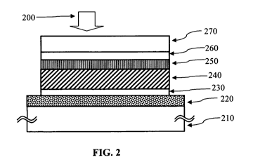
[0015] FIG 2 shows a general schematic of a side view of one embodiment of the
invention depicting a substrate CdTe solar cell with an interface layer
between the
absorber and the window layer
[0016] FIG 3 shows a general schematic of a side view of one embodiment of the
invention depicting a deposition system that allows the deposition of CdTe
films
comprising varying grain sizes.
[0017] FIG 4 shows a general schematic of a side view of one embodiment of the
invention depicting a film grain structure in the absorber layer.
[0018] FIG 5 shows a general schematic of a side view of one embodiment of the
invention depicting a deposition system that allows the deposition of a
CdTe/CdTel_
,,S,,/CdS device structure without vacuum break.
DETAILED DESCRIPTION OF THE EMBODIMENTS
[0019]Reference will now be made in detail to some specific embodiments of the
invention including the best modes contemplated by the inventors for carrying
out the
invention. Examples of these specific embodiments are illustrated in the
accompanying
drawings. While the invention is described in conjunction with these specific
embodiments, it will be understood that it is not intended to limit the
invention to the
described embodiments. On the contrary, it is intended to cover alternatives,
8
CA 02718272 2010-09-10
WO 2009/120340 PCT/US2009/001874
modifications, and equivalents as may be included within the spirit and scope
of the
invention as defined by the appended claims. In the following description,
numerous
specific details are set forth in order to provide a thorough understanding of
the present
invention. The present invention may be practiced without some or all of these
specific
details. In this specification and the appended claims, the singular forms
"a," "an," and
"the" include plural reference unless the context clearly dictates otherwise.
Unless
defined otherwise, all technical and scientific terms used herein have the
same meaning
as commonly understood to one of ordinary skill in the art to which this
invention
belongs.
[0020] "Interface layer" as used herein is meant to include a layer or
plurality of layers
between the absorber layer and the window layer. By definition an "interface
layer"
includes a single layer as well as a set of multiple layers which may be 1, 2,
3, 4, 5 or
more layers. Each layer or layers may independently comprise a thin film,
nanoparticles,
sintered nanoparticles or a combination of one or more of the three. Also, the
invention
contemplates that a plurality of interface layers comprising films with the
same and/or
different grain sizes as well as layers comprising nanoparticles, sintered
nanoparticles and
or thin films of different chemical compositions.
[0021] As used herein the metal electrode is also referred top as a "back
contact" or
"electrode".
[0022] By "photovoltaic device" as used herein it is meant a multilayered
structure
comprising the layers necessary where in a working environment with proper
leads and
connections is capable of converting light into electricity. In one embodiment
the device
contains at least the following layers in order: a substrate/electrode layer
/absorber
9
CA 02718272 2010-09-10
WO 2009/120340 PCT/US2009/001874
layer/interface layer/window layer and a TCO layer and this structure is known
in the art
as a "substrate configuration". In a substrate configuration the substrate may
be
transparent or opaque. In a preferred embodiment the substrate comprises a
metal and is
opaque. The device may have any further structure necessary to practically
utilize the
device such as leads, connections, etc. The above preferred embodiments of the
present
invention do not limit the order of layers or deposition order of the
photovoltaic device.
[0023] The absorber layer used in conjunction with solar cells of the present
invention
comprises Group II-VI semiconductor compound materials. The window layer used
in
conjunction with the instant invention preferably comprises n-type material.
The window
layer may comprise those materials known in the art such as CdS, CdSe, ZnS,
ZnSe and
oxysulfides.
[0024] By "grain size" it is meant grains having an average grain size
diameter as
measured by viewing a cross section of the layer with an electron micrograph
(SEM or
TEM). A number of grains, for example 30, are selected because their cross
section
represents the diameter of the grain and not a partial cross section, and the
thicknesses of
the selected grains are measured at their thickest point. An average thickness
of the
selected grains is calculated and this is the average grain size diameter.
[0025] By "small grain sizes" it is meant grain sizes having a diameter of
between about
0.1 and 1.0 gm.
[0026] By "large grain sizes" it is meant grain sizes having a diameter of
between about
2-6 m.
CA 02718272 2010-09-10
WO 2009/120340 PCT/US2009/001874
[0027] By "plurality of grain sizes" it is meant particles having more than
one grain size.
In one embodiment the invention contemplates that a there be a population of
small grain
sizes and a population of large grain sizes.
[0028] By "surface treatment" it is meant to include the processes wet
etching, dry
etching, sputtering, reduction, electrochemical, heat treatments and ion
milling. These
examples are illustrative only and not exhaustive.
[0029] By "buried junction" it is meant a p-n junction located away from (i.e.
not directly
contacting) the interface of the window and absorber layers. The invention
contemplates
that a buried junction may extend into the absorber layer or into the
interface layer.
[0030] By "forming a layer" it is meant those steps for depositing, etching,
reacting
scribing or otherwise creating or adding to a layer, or acting on a layer
already present.
[0031 ] By "forming a buried junction in the absorber layer" it is meant those
steps
necessary to create a buried junction.
[0032] Nanoparticles or sintered nanoparticles useful in the present invention
comprise
compound semiconductors which include Group I-VI, II-VI, III-V and IV-VI
compounds
and Group IV semiconductors. This also includes 1-111-VI compounds such as
CIGS.
CIGS is CuIn,,Ga1_XSe, where 0 x<1 and included herein is the family of
materials known
in the art as CIGS including CIS, CISe, CIGSe, CIGSSe. Spherical nanoparticles
used
herein have a size between about 1-100 nm, preferably between about 2-20 nm.
It is
understood that the instant invention contemplates that "nanoparticles" as
used herein is
not limited to spherical or substantially spherical particles but includes
various shaped
nanostructures such as tetrapods, bentrod, nanowires, nanorods, particles,
hollow
particles, single materials, alloyed materials, homogeneous and heterogeneous
materials.
11
CA 02718272 2010-09-10
WO 2009/120340 PCT/US2009/001874
The size of the nanoparticles is variable but it is preferred that if the
particle is an
elongate structure, i.e. a nanorod, that the length of the nanorod have a
maximum length
of about 100 urn and have a maximum diameter of about 1-20 nm, preferably
about 5nm.
[0033] Nanoparticles or sintered nanoparticles according to the instant
invention may
have a core or core/shell or core/shell/shell, or core/shell/shell/shell
construction. The
core and/or the shell can be a semiconductor material including, but not
limited to, those
of the Group II-VI (ZnS, ZnSe, ZnTe, CdS, CdSe, CdTe, HgS, HgSe, HgTe, MgTe
and
the like) and Ill-V (GaN, GaP, GaAs, GaSb, InN, InP, InAs, InSb, AlAs, AlP,
AlSb, AIS,
and the like), Group IV-V compounds, and IV (Ge, Si) materials, and an alloy
thereof, or
a mixture thereof. Type II heterostructures (see S. Kim, B. Fisher, H.J.
Eisler, M.
Bawendi, Type-II quantum dots: CdTe/CdSe(core/shell) and CdSe/ZnTe(core/shell)
heterostructures, J. Am. Chem. Soc. 125 (2003)11466-11467, the contents of
which are
incorporated herein by reference) and alloyed quantum dots (X.H. Zhong, Y.Y.
Feng, W.
Knoll, M.Y. Han, Alloyed Zn,,Cdi -,,S nanocrystals with highly narrow
luminescence
spectral width, J. Am. Chem. Soc. 125 (2003) 13559-13563 and R.E. Bailey, S.M.
Nie,
Alloyed semiconductor quantum dots: tuning the optical properties without
changing the
particle size, J. Am. Chem. Soc. 125 (2003) 7100-7106, the contents of both
are
incorporated herein by reference) are considered suitable. The nanoparticles
or sintered
nanoparticles may have coatings or ligands attached thereto. Most of the
materials listed
above are quantum confined. But the invention does not require that the
nanoparticles be
quantum confined.
[0034] The invention contemplates that the nanoparticles used herein may be
sintered or
unsintered. In one embodiment of the present invention the nanoparticles are
sintered or
12
CA 02718272 2010-09-10
WO 2009/120340 PCT/US2009/001874
partially sintered during manufacturing and thus and the device comprises
"sintered
nanoparticles" or "nanoparticles that are sintered". One of ordinary skill in
the art will
appreciate that the sintering process will alter the morphology, size and
shape of the
nanoparticles. Nanoparticle interface layers according to this invention can
be thermally
processed (in air, inert or reducing atmosphere or vacuum) to improve their
electrical
properties. Other sintering methods include laser, rapid thermal processing,
flash
annealing and similar techniques.
[0035] In one embodiment of the present invention there is disclosed an
increased
efficiency solar device obtained by controlling the grain size of the absorber
and/or
interface layer. The morphology and grain size of the interface and/or
absorber layer
significantly influences the diffusion of window layer materials into the
absorber layer,
for example CdS into CdTe. Group H-VI absorber material films possessing very
large
grains such as 2-6 m or even a larger distribution of 5-6 m gains exhibit
minimal bulk
diffusion of window materials into a Group II-VI absorber layer because the
diffusion is
predominantly one dimensional. This is undesirable. If the grains at the
surface of the
absorber layer or in an interface layer are smaller as contemplated in one
embodiment of
the present invention, for example 0.1 to 1.0 m, the bulk diffusion is
enhanced
significantly because the increased grain boundary diffusion of the smaller
grains allows
a window layer compound, for example CdS to diffuse from all sides of the
grains
producing three dimensional diffusion. Three dimensional diffusion can also
result in a
CdTe-CdS buried junction around the grains increasing the junction area
resulting in high
efficiency devices.
13
CA 02718272 2010-09-10
WO 2009/120340 PCT/US2009/001874
[0036] In a preferred embodiment of the present invention an interface layer
is located
between the absorber layer and the window layer comprising an alloy of a Group
II-VI
compound and Sulfur. While not wishing to be bound by any particular theory or
principle it is believed the interface layer reduces the interface states
density resulting
from a 10% lattice mismatch between a window layer material such as CdS and a
Group
II-VI absorber material like CdTe by grading the lattice constants and also
allowing the
formation of a buried homo-junction in the absorber layer. Inter-diffusion of
CdS and
CdTe is essential to buffer the close to 10% lattice mismatch between CdS and
CdTe by
the formation of a CdTei_,,S,, alloy layer. This inter-diffusion also results
in a buried
electrical junction away from the CdS-CdTe metallurgical junction, which
reduces the
deleterious effects of interface states resulting from lattice mismatch. While
not wishing
to be bound by any particular theory this is probably because the formation of
CdTe1,S,,
is less efficient compared to significant amount of grain boundary diffusion
and loss of S
by sublimation.
[0037] A prior art solar device having a substrate device configuration is
shown in FIG 1.
Substrate 110 faces away from the sun 100 to generate photovoltaic output.
Metal
electrodes 120 are deposited on the substrate 110 using known techniques.
Since it is not
possible for any known metal electrode to form ohmic contacts with CdTe
interface layer
130 may be deposited on the metal electrode 120 prior to CdTe deposition, see
commonly assigned Hotz et al., U.S. Published Application No. filed March 13,
2009, currently pending which claims priority to U.S. Provisional Serial No.
61/070,006
filed March 18, 2008, and commonly assigned Hotz et al. U.S. Published
Application No.
filed March 13, 2009, currently pending, which claims priority to U.S.
Provisional
14
CA 02718272 2010-09-10
WO 2009/120340 PCT/US2009/001874
Serial No. 61/069,952 filed March 18, 2008 the contents of both are hereby
incorporated
by reference. A CdTe absorber 140 layer is then deposited. A junction is
formed by
depositing a CdS window layer 160 using a PVD process such as sputtering or
evaporation. A transparent contact usually a transparent conducting oxide
(TCO) material
layer 170 is deposited on the CdS to complete the solar cell.
[0038] An embodiment of the present invention incorporating an interface layer
between
the absorber layer and the window layer is depicted in FIG 2. The substrate
210 is coated
with a metallic electrode 220 by means of deposition techniques known in the
art. The
metal electrode 220 can be Mo, Ti, Al or other electrode metals. Preferred is
Mo or Ti.
The metal electrode layer 220 thickness can be 200-2,000 nm. The substrate 210
can be
transparent such as glass, translucent such as polymer or opaque such as metal
foil of Al,
Ti, Cu, Mo or stainless steel. Preferred is stainless steel, Ti or Mo. Back
contact layer
230 is then deposited by a PVD process such as sputtering or evaporation or by
means of
printing and sintering the nanoparticles. Back contact layer materials can be
those
disclosed in the art see commonly assigned patent application Hotz et al.,
U.S. Published
Application No. filed March 13, 2009, currently pending which claims priority
to
U.S. Provisional Serial No. 61/070,006 filed March 18, 2008, and commonly
assigned
Hotz et al. U.S. Published Application No. , filed March 13, 2009, currently
pending, which claims priority to U.S. Provisional Serial No. 61/069,952 filed
March 18,
2008, which provide advantages in contacting absorber materials such as CdTe
which do
not form ohmic contacts directly with metals. A CdTe absorber layer 240 with
thickness
1-10 m is deposited on top of the interface 230 using PVD processes such as
Close
Spaced Sublimation (CSS), sputtering or by coating with a CdTe nanoparticle
ink by
CA 02718272 2010-09-10
WO 2009/120340 PCT/US2009/001874
means of coating methods known in the art such as inkjet, die coating, blade
coating or
spraying followed by sintering. The CdTe layer 240 can be subjected to a CdCl2
treatment to increase the grain size prior to further processing.
[0039] Referring to FIG 2 a CdTe deposition is followed by the interface layer
250 and
the window layer 260. The preferred thickness of the window layer 260 is from
0.1 to
0.2 m. A greater thickness would result in optical loss due to increased
absorption in the
window layer 260. The thickness of the interface layer 250 is about 0.01 gm to
1.0 gm,
preferably 0.1 gm to 0.5 m. TCO layer 270 usually comprises ZnO doped with
group III
elements such as Al, Ga or and deposited using techniques such as sputtering.
A bilayer
TCO 270 comprising an insulation layer such as undoped ZnO and a conducting
layer
such as doped ZnO would help to increase the Voc of the device. The thickness
of the
insulation layer (not shown) may be 0.04 to 0.1 m while the conducting layer
may be
0.2 to 0.4 m thick.
[0040] In one embodiment of the present invention the CdTe absorber layer (or
an
interface layer material) grain size can be controlled by controlling the
substrate
temperature during the evaporation process. While not wishing to be bound by
an exact
temperature/grain profile, a 450 C substrate temperature during close spaced
sublimation
may result in CdTe films having grains sizes about .20 m to 2.0 m. A 620 C
substrate
temperature during close spaced sublimation of CdTe may result in CdTe films
with
grain size of about 2.0-6.0 m. The invention contemplates a temperature range
of
between 300 C to 620 C. The invention prefers large grain sizes to be between
2.0-3.0
gm. In another embodiment of the present invention a temperature profile
comprising
high and low substrate temperatures such as 620 C followed by 450 C can be
used to
16
CA 02718272 2010-09-10
WO 2009/120340 PCT/US2009/001874
create a graded layer of grain sizes with a size reduction towards the
CdTe/window layer
junction in a continuous deposition process.
[00411 FIG 3 shows an embodiment of the close spaced sublimation deposition
apparatus
of Group H-VI films that enable Group II-VI compound grain sizes tailored in
accordance with the present invention. Herein there is disclosed grain size
growth in an
interface layer but the invention contemplates equally well the formation of
grain size
growth in the absorber layer. CdTe is the preferred Group II-VI semiconductor
compound. The deposition system includes CdTe sublimation sources 320 and
fluxes
340 separated by thermal insulators 330 to reduce the thermal cross talk
between the
sources. The substrate 300 is heated using substrate heaters 311, 312 and 313
in the close
proximity to the substrate 300. The direction of the substrate transport is
shown by arrow
380. However, the invention also allows for reverse substrate deposition. The
deposition
starts at a high substrate temperature and reduces to a lower temperature to
enable the
formation of smaller grains on the CdTe film surface 350 by varying the
substrate heater
311, 312 and 313 temperatures. Preferably the higher substrate temperature is
about
550 C to about 650 C and the low temperature is about 400 C to about 450 C.
The low
temperature may be lower, depending on the Group II-VI compound or the window
layer
compound. As low as 300 C is contemplated. In another embodiment CdTe films
with
uniformly small grains can be deposited by reducing the substrate heater
temperature on
all heaters 311, 312 and 313.
[0042] In another embodiment of the present invention there is contemplated a
two step
sintering process employed to create similar grain morphology in either an
absorber layer
or an interface layer. A dispersion of nano or submicron size Group H-VI
compound
17
CA 02718272 2010-09-10
WO 2009/120340 PCT/US2009/001874
(preferably CdTe) particles are dispensed and sintered at a high temperature
followed by
another dispensing of the same Group II-VI dispersion that annealed at a lower
temperature. In one non-limiting example the thickness of the grains in the
first layer can
be between 2-6 gm, preferably 2-3 m, and the second layer can be 0.05 to
01.05 m. The
grain size distribution of particles in each layer is low and the invention
contemplates that
most layer will have a closes grain size distribution. The substrate
temperature for the
first layer can be 550 C to 600 C and the second layer can be 450 C to 500 C
[0043] FIG 4 shows the schematic of the grain structure that result from one
embodiment
of a CdTe deposition shown in FIG 3. The higher substrate temperature during
the initial
phase of the deposition results in larger grains 420. It is preferred that
these grain sizes be
about 2-6, preferably 2-3 gm, with a narrow distribution of sizes. The lower
substrate
temperature towards the end of the deposition results in smaller grains 430.
Preferably the
size of the small particles is between 0.1 and 1.0 m, with a narrow
distribution of sizes in
an individual layer, preferably the sizes are within 10%. The invention
contemplates that
the grain sizes are not limited to one or two layers but that there may be a
gradation of
grain sizes of three or more. The invention prefers that the smallest grain
size be on the
top layer of any stack of plurality of grain sizes and closest to the window
layer, the
interface layer or the junction, depending on the device construction. The
invention
contemplates that the grain sizes not be restricted to an interface layer but
may also be in
the absorber layer. For example a top portion of the absorber layer may
comprise
particles having a small diameter.
18
CA 02718272 2010-09-10
WO 2009/120340 PCT/US2009/001874
[0044] The invention described herein contemplates three different processes
to obtain
the interface layer with lattice constants engineered to reduce the interface
states. It is
understood that these embodiments are illustrative but not exhaustive.
[0045] In one embodiment of the present invention a window layer comprising
for
example CdS with a thickness of about 0.1 to 0.15 m is deposited on a CdTe
film with a
Cd rich surface or surface with small CdTe grains (after low temperature CdTe
deposition). The films are then annealed at a temperature ranging from 400 C
to 550 C
for a10 to 30 min duration. This temperature treatment can also be carried out
in the
presence of CdC12 vapor from either a vapor source or CdC12 applied directly
on CdS
surface using a saturated solution of CdC12 in methanol. The effect of CdC12
and
temperature on CdS diffusion during device processing is known see "Study of
in-situ
CdC12 treatments on CSS deposited CdTe films and CdS/CdTe solar cells " P.D.
Paulson
and V.Dutta, Thin Solid films, 370, 2000, pp 299- 306 the contents of which
are
incorporated herein by reference.
[0046] In another embodiment of the present invention an interface layer is
created by
depositing a Group II-VI absorber layer followed by the deposition of a Group
II-VIat_
XVI' compound, a fib, alloy with x varying from 0 to 1 forming a gradient of
pure CdTe
near the absorber layer and pure CdS near the window layer. This is
particularly suitable
for a continuous roll to roll fabrication of the device structure without a
vacuum break.
Thermal sources can be arranged in such a way that the flux changes from pure
CdTe
through CdTe deposition followed by interface layer where x varies from 0 to 1
followed
by the deposition of pure CdS flux for the CdS film deposition. During this
deposition,
the substrate temperature is changed from 550 C - 650 C for CdTe deposition to
250 C-
19
CA 02718272 2010-09-10
WO 2009/120340 PCT/US2009/001874
350 C during interface layer deposition and finally to 200 C to 300 C for CdS
deposition. Depending on the material, temperatures higher than 400 C during
or after
the interface layer deposition could result in a segregation of secondary
phases in the
interface layer because of the miscibility gap in the CdS-CdTe phase diagram.
The
solubility of Sulfur in CdTe is only 5.8% see "Thin Film Cadmium Telluride -
Cadmium
Sulfide alloys and devices " D. G. Jensen, B.E. McCandless and R. W. Birkmire,
25th IEEE
Photovoltaic Specialist Conference, 1996, pp 773-776 the contents of which are
incorporated herein by reference. Because of this reason the interface layer
approach
described in this invention is not suitable for a superstrate configuration,
where the CdTe
deposition temperature exceeds 450 C temperature.
[0047] A low temperature deposition of a Group II-VIa1_XVIbX compound, a fib,
where
0<x<l, for example CdTe1_XSX where 0<x<l, followed by the heat treatment at
temperature >400 C prior to CdS deposition can also be used to precipitate the
CdS to
the CdTei_XSX grain boundary and forming three dimensional junction of
CdTe94.6S5.8/CdS.
[0048] In a third embodiment multiple thin films comprising various
stoichiometric
amounts of a Group II-Vlal_XVIbX compound, a #b where 0<x<l,for example,
CdTel_XSX
with x varying from 0 to I is dispensed using a dispersion of CdTel_,,SX nano
or sub
micron particle on surface treated CdTe film. The film stack is then heat
treated at
temperature 250 C to 450 C in an inert ambient. This temperature treatment can
also be
carried out in the presence of CdC12 vapor from either a vapor source or CdC12
applied
directly on CdS surface using a saturated solution of CdC12 in methanol.
CA 02718272 2010-09-10
WO 2009/120340 PCT/US2009/001874
[0049] In a preferred embodiment the interface layer comprises a
stoichiometric gradient
of CdTei_XSX composition where 0<x<1 between CdTe and CdS.
[0050] In another alternative embodiment of the present invention there is
contemplated
various stoichiometric amounts of Group II-VIa1_XVIbX compound where alb and
0<x<1,
for example, CdTeI_XSe,t is dispensed using a dispersion of CdTe1_XSe,t nano
or sub
micron particle on a surface treated CdTe film. The film stack is then heat
treated at
temperature 250 C to 450 C in an inert ambient. This temperature treatment can
also be
carried out in the presence of CdCl2vapor from either a vapor source or CdC12
applied
directly on CdS surface using a saturated solution of CdC12 in methanol.
[0051 ] It is preferred that the CdTe surface undergo treatments prior to
deposition of the
CdS window layer as well as thermal treatment after the deposition of the CdS
window
layer. In one embodiment the treatment removes native oxides such as CdTeO3,
or CdO
from the CdTe surface. This treatment is particularly significant for a batch
production
process that involves a vacuum bake or exposure of the CdTe surface to an
oxidizing gas
ambient in the production process resulting in the formation of oxides. Wet as
well as
dry processes can be used for this process. A short wet etch in Br-methanol
solution can
be used to remove the surface oxides, see "The dynamics of Cadmium Telluride
Etching"
K.D. Dobson, P.D. Paulson, B.E. McCandless and R.W. Birkmire, Mat. Res. Soc.
Symp.
Proc. Vol. 763, 2003, pp B3.1.1- 12 the contents of which are incorporated
herein by
reference. Sputtering, reduction in hydrogen plasma or heat treatments in
Hydrogen or
forming gas is particularly suitable for the dry process. Sputter process
parameters such
as process pressure, sputter power are tweaked to reduce the sputter damage on
the CdTe
surface. Previously sputter cleaning has been employed to clean the CdTe
surface prior
21
CA 02718272 2010-09-10
WO 2009/120340 PCT/US2009/001874
to contacting with metal electrode see " RF sputtering as a surface cleaning
process for
CdTe solar cells" V. Viswanathan, D.L. Morel and C.S.Ferekides, 31st IEEE
Photovoltaic Specialist conference, 2005, pp 426-429 the contents of which are
incorporated herein by reference. High process pressure such as 150 to 400
mTorr and
low sputter power such as 30-100 watts inch is particularly suitable for the
removal of
oxides.
[0052] Another embodiment of the present invention envisions a surface
treatment to
remove the accumulation of deleterious trace elements on the absorber layer
surface that
diffused from the metal substrate as a result of the high temperature CdTe
deposition. For
example, Cu from a Cu doped ZnTe interface layer between the metal back
contact and
the absorber layer can diffuse through CdTe grain boundaries during CdTe
deposition
and create acceptor states in window layer and thereby compensate the n-type
dopants.
Previous studies show that Cu concentration higher than 1020/cm3 in CdS would
severely
affect the device results, see "Introduction of Cu in CdS and its effect on
CdTe/CdS solar
cells" K. Barri, M. Jayabal, H.Zhao, S. Asher, J.W. Pankow, M.R. Young and
C.S.
Ferekides, 30 IEEE Photovoltaic Specialist conference, 2005, pp 287-290, the
contents
of which are incorporated herein by reference. As a remedy preferential
sputtering
provides means to selectively sputter clean the trace elements. For example,
Cu has
higher sputter yield with respect to CdTe and hence traces of these elements
can be
preferentially sputtered. Selection of sputter power and the process pressure
is very
crucial for the selectively sputtering the trace elements without damaging the
CdTe
surface. For example a high sputter power density such as 100 to 200
watts/inch2 and low
process pressure such as 1-2 mTorr would result in sputter damages on CdTe
surface
22
CA 02718272 2010-09-10
WO 2009/120340 PCT/US2009/001874
which results in heavily compensated surface regions with very low acceptor
density. A
preferred sputter clean process employs a low sputter power (1-2 watts/square
inch) to
reduce the sputter damage and higher process pressure (15-20mTorr) to increase
the
scattering and thereby reduce the sputter damage and also increase the
sputtering from
grain boundaries. Adding forming gas in to the sputter gas aids in removing
both oxides
as well as the metal traces. Assuming that all the Cu traces has been diffused
to the CdTe
surface during and later removed by the sputter cleaning process, a high
temperature
annealing process can be used to anneal out all the sputter damage prior to
the CdS
deposition.
[0053] Another embodiment of the present invention contemplates a treatment to
create
Group VI vacancies in the absorber layer, for example Te vacancies in a CdTe
absorber
layer. This advantageously enhances sulfur diffusion to CdTe lattice. The
surface
treatment described here creates a Te depleted CdTe surface to enhance the
formation of
CdTei_XSX alloy formation during subsequent CdS deposition. The invention
contemplates that a wet as well as a dry process can be employed to create a
Cd rich
surface. For example selective electro chemical dissolution of Te by using
suitable
electropotential can be employed to create a Cd rich surface. This is possible
because the
standard electrode potential of Te (+0.55V) is more positive compared to Cd (-
0.4V). Dry
process has its own advantages and hence Ion milling which has been employed
in the
past on superstrate configuration device prior to contact application becomes
an ideal
candidate. Ion milling results shows that the resulting CdTe surface
composition depends
on the ion milling time and it has been employed to create Te rich surface see
"Studies of
ZnTe back contacts to CdS/CdTe solar cells" T.A. Gessert, P. Sheldon, X.Li, D.
23
CA 02718272 2010-09-10
WO 2009/120340 PCT/US2009/001874
Dunlavy, D. Niles, 26th IEEE Photovoltaic Specialist conference, 1997, pp 419-
422, the
contents of which are incorporated herein by reference. In another embodiment
of the
present invention there is contemplated an interface layer comprising a Te
rich CdTe
composition that may be used advantageously to block Cu migration.
[0054] FIG 5 shows an embodiment of a close spaced sublimation deposition
system of
Group II-VI films that enable the deposition of a an absorber layer,
preferably comprising
CdTe, an interface layer having a Group II-VI-S gradient, preferably a CdTeS
gradient
followed by the CdS window layer to form a full device structure in a
continuous fashion
without vacuum break. The deposition system includes CdTe sublimation sources
520,
521, 522 and 523, a CdTe0.5S0.5 source 524 and CdS source 525 separated by
thermal
insulators 560 to reduce the thermal cross talk between the sources. In close
proximity to
the substrate 500 are heaters 510, 511, 512 and 513 for implementing various
heating
profiles to the substrate. The invention contemplates that any number of
heaters may be
employed. In a preferred embodiment the deposition starts at high substrate
temperature
at heater 510 (550 C to 650 C) and maintained at high temperature during CdTe
deposition and is reduced to a low temperature (250 C to 350 C) during the
interface
layer deposition and further reduced to 200 C to 300 C range during the CdS
layer
deposition. The mixing of the fluxes 570 from sources 523, 524 and 525 allows
the
formation of an interface layer having a graded composition comprising
CdTe,,Si_,, where
0<x<1 interface layer. The invention contemplates the mixing of the fluxes 571
from
sources 523 (CdTe) and 524 (CdTeo.5So.5) (as non limiting examples of source
compositions) as well as the mixing of the fluxes 573 from sources 524
(CdTeo.5So.5) and
525 (CdS) will result in films having stoichiometric gradations of the
CdTel_XS,,. The flux
24
CA 02718272 2010-09-10
WO 2009/120340 PCT/US2009/001874
mixing 571 and/or 572 is generally not uniform. Fluxes may be mixed, for
example by
moving sources close enough to one another. This may be about I or 2 inches
but may be
less or more depending on the deposition parameters. For a high vacuum process
they
sources may be farther apart. Also by using the temperature profile mentioned
above the
composition grading in the interface layer is retained without the formation
of secondary
phases. Non-limiting methods to mix the flux include changing the temperature
of any of
the sources which will raise or lower the flux concentration. Changing the gap
of the
source to substrate will change the mixed flux composition as well. More gas
pressure
results in more flux mixing. Changing the temperature of the heating elements
510, 511,
512 and 513 will result in a different sticking coefficient for each substrate
location and
by producing a gradation of temperature with the four (or more) heaters the
deposited
composition may have a graded stoichiometric composition. The deposition
scheme
described here not limited to CSS and in fact it also work with any other PVD
techniques
such as Laser ablation, sputtering or high rate vapor deposition etc.